lecture 10: small signal device parameters - · pdf filelecture 10: small signal device...
TRANSCRIPT

Lecture 10: Small Signal Device Parameters
2016-02-09 1Lecture 9, High Speed Devices 2016

Lecture 12: Ballistic FETs
2016-02-09 2Lecture 9, High Speed Devices 2016
Liu: 220-222, 239-242

Large Signal / Small Signal
2016-02-09 3Lecture 9, High Speed Devices 2016
vcb
Vcb
vbe
VBE
ie+IE ic+IC
cbbeCcb
VCB
be
VBE
CBBEcCC
cbbeEcb
VCB
be
VBE
CBBEeEE
vyvyIvV
fv
V
fVVfiIi
vyvyIvV
fv
V
fVVfiIi
BECB
BECB
222122
2
121111
1
,
,
The electrical signal is often small.
Divide the total voltage/currentinto a large (DC) and small (AC) signal. We are mainly interested in the small signal part.
Bias Current Signal Current
We can make a Taylor expansion around the bias voltage.Non-linear constant bias current voltage and linear AC varying signal current/voltage.

2 port – y-parameters
2016-02-09 4Lecture 9, High Speed Devices 2016
cb
VCB
be
VBE
CBBEcCC
cb
VCB
be
VBE
CBBEeEE
vV
fv
V
fVVfiIi
vV
fv
V
fVVfiIi
BECB
BECB
112
111
,
,
2
1
2221
1211
2
1
v
v
yy
yy
i
i
v1 v2
i1 i2+
-
+
-
2-port
01
111
2
vv
iy
02
112
1
vv
iy
i1 i2
v1
+
-
v2
+
-
E C
B
…
2
1
2
1
2221
1211
2
1
1
2221
1211
v
v
i
i
zz
zz
i
i
yy
yyCan transform to different parameter sets

Y,z,ABCD,h,g
2016-02-09 5Lecture 9, High Speed Devices 2016
2
1
2221
1211
2
1
v
v
yy
yy
i
i
2
1
2221
1211
2
1
i
i
zz
zz
v
v
2
2
1
1
i
v
DC
BA
i
v
2
1
2221
1211
2
1
v
i
hh
hh
i
v
2
1
2221
1211
2
1
i
v
gg
gg
v
i
ABCD/ cascade/ a-parameters Hybrid parameters
Inverse hybrid parameters
Admittance Impedance
1
1
2221
1211
2
2
i
v
bb
bb
i
v
b-parameters

Conversion between parameter sets
2016-02-09 6Lecture 9, High Speed Devices 2016
From Electric Circuits, J. W. Nilsson and S.A. Riedel

Shunt/Series addition
2016-02-09 7Lecture 9, High Speed Devices 2016
v1 v2
+
-
+
-
ya
yb
Shunt
- -
za
v1
i1i2
+ +
zb
Series
v1 v2
i1 i2+
-
+
-
yc
𝑦𝑐 = 𝑦𝑎 + 𝑦𝑏 𝑧𝑐 = 𝑧𝑎 + 𝑧𝑏
v1 v2
i1 i2+
-
+
-
zc
v2

Cascade, Serier/Parallel additions
2016-02-09 8Lecture 9, High Speed Devices 2016
v1 v2
+
-
+
-
ABCDa ABCDb
Cascade
- -
ha
v1
i1i2
+ +
hb
Series/parallel
v1 v2
i1 i2+
-
+
-
ABCDc
𝐴𝐵𝐶𝐷𝑐 = 𝐴𝐵𝐶𝐷𝑎 + 𝐴𝐵𝐶𝐷𝑏ℎ𝑐 = ℎ𝑎 + ℎ𝑏
v1 v2
i1 i2+
-
+
-
hc
v2
g-parameters parallel/series: gc=ga+gb

DC y-parameters models
2016-02-09 9Lecture 9, High Speed Devices 2016
𝑖𝑔𝑖𝑑
=0 0𝑔𝑚 𝑔𝑑
𝑣𝑔𝑠𝑣𝑑𝑠
=𝑦𝑔𝑔 𝑦𝑔𝑑𝑦𝑑𝑔 𝑦𝑑𝑑
𝑣𝑔𝑠𝑣𝑑𝑠
𝑖𝑏𝑖𝑐
=
𝐼𝑐𝛽𝑉𝑡
0
𝐼𝐶𝑉𝑡
0
𝑣𝑏𝑒𝑣𝑐𝑒
=𝑦𝑏𝑏 𝑦𝑏𝑐𝑦𝑐𝑏 𝑦𝑐𝑐
𝑣𝑏𝑒𝑣𝑐𝑒
vbe
vgs
vce
vds
ib
ig
ic
id
vsg vdg
is idIf we know the y-parameters for one configuration we can calculate the y-parameters for a different configuration!

Indefinite Admittance Matrix
2016-02-09 10Lecture 9, High Speed Devices 2016
c
b
e
cb
bcbbbe
eb
c
b
e
v
v
v
y
yyy
y
i
i
i
ccce
ecee
yy
yy
vb
ie ic
ib
If ve=vc=vb=v : how large is ie ib and ic?
Why is yce+ycb+yec=0
vcve
If ve=v and vb=vc=0 : how large is ie+ib+ic?
Why is yee+ybe+yce=0All rows and columns have to sum up to zero!
1 3
2
CE: ybb,ybc,ycb,ycc
CB: yee,yec,ycc,yce

CS/CC/CG – CS/CD/CG configurations
2016-02-09 11Lecture 9, High Speed Devices 2016
Same for FETsbut with:
C DE SB G
From Radio Electronics, L. Sundström, G. Jönsson and H. Börjesson

Y-parameters for common gate transistor
2016-02-09 12Lecture 9, High Speed Devices 2016
vsg vdg
is id𝑖𝑠𝑖𝑑
=𝑔𝑚 + 𝑔𝑑 −𝑔𝑑
−(𝑔𝑚 + 𝑔𝐷) 𝑔𝑑
𝑣𝑠𝑔𝑣𝑑𝑔
=𝑦𝑠𝑠 𝑦𝑠𝑑𝑦𝑑𝑠 𝑦𝑑𝑑
𝑣𝑠𝑔𝑣𝑑𝑔
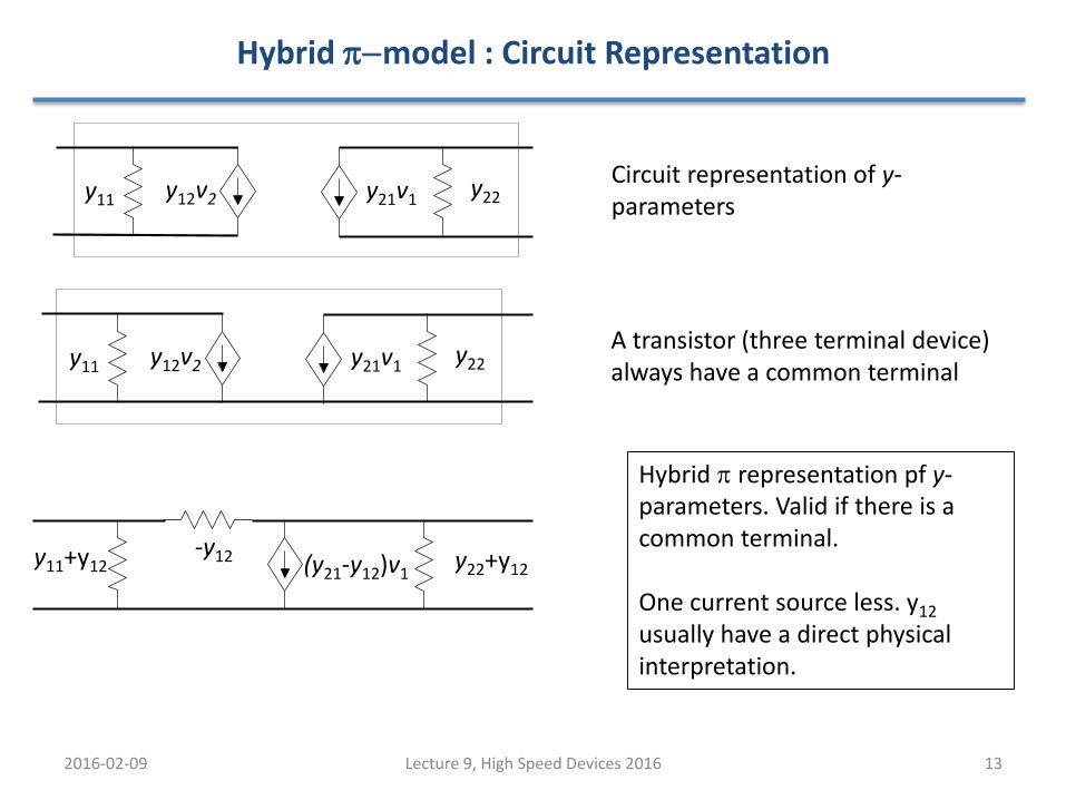
Hybrid pmodel : Circuit Representation
2016-02-09 13Lecture 9, High Speed Devices 2016
y11y22y21v1y12v2
y11+y12 y22+y12(y21-y12)v1
Circuit representation of y-parameters
Hybrid p representation pf y-parameters. Valid if there is a common terminal.
One current source less. y12
usually have a direct physical interpretation.
y11y22y21v1y12v2
A transistor (three terminal device) always have a common terminal
-y12
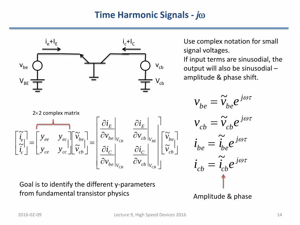
Time Harmonic Signals - jw
2016-02-09 14Lecture 9, High Speed Devices 2016
vcb
Vcb
vbe
VBE
ie+IE ic+IC Use complex notation for small signal voltages. If input terms are sinusodial, the output will also be sinusodial –amplitude & phase shift.
w
w
w
w
j
cbcb
j
bebe
j
cbcb
j
bebe
eii
eii
evv
evv
~
~
~
~
cb
be
Vcb
C
Vbe
C
Vcb
E
Vbe
E
cb
be
ccce
ecee
c
e
v
v
v
i
v
i
v
i
v
i
v
v
yy
yy
i
i
CBCB
BECB
~
~
~
~
~
~
Goal is to identify the different y-parameters from fundamental transistor physics
22 complex matrix
Amplitude & phase

Complex small signal parameters
2016-02-09 15Lecture 9, High Speed Devices 2016
𝑖𝑔𝑖𝑑
=𝑗𝜔𝐶𝑔𝑔 −𝑗𝜔𝐶𝑑𝑔
𝑔𝑚 − 𝑗𝜔𝐶𝑑𝑔 𝑔𝑑 + 𝑗𝜔𝐶𝑑𝑑
𝑣𝑔𝑠𝑣𝑑𝑠
=𝑦𝑔𝑔 𝑦𝑔𝑑𝑦𝑑𝑔 𝑦𝑑𝑑
𝑣𝑔𝑠𝑣𝑑𝑠
We will determine that the y-parameters can be written as real an imaginary parts, with the imaginary parts corresponding to capacitive elements.
• Where gm, Cgg, Cdg originates from the physics of the transistor.
• The different parameters thus depend of w, VGS, VDS and the geometry of the transistors.
Intrinsic (quasi static) y-parameters for a FET.

Current Gain – h21
2016-02-09 16Lecture 9, High Speed Devices 2016
v1 v2
i1 i2+
-
+
-
2-port
Maximum current gainv2 is short circuited
ℎ21 =𝑖2𝑖1𝑣2=0
ℎ21 =𝑖2𝑖2𝑣2=0
=𝑦21𝑦11
𝑖1 = 𝑦11𝑣1 𝑖2 = 𝑦21𝑣1 Apply a test voltage to the in-port:
The current gain typicially decreases with frequencyℎ21 = 1 corresponds to the transition
frequency , 𝒇𝑻.

Power Gain I – Transducer Gain
2016-02-10 17Lecture 9, High Speed Devices 2016
2-port yL
Pav,s
PL Power available from source: Pav,s
Power delivered at load: PL
𝐺𝑇 =𝑃𝐿𝑃𝑎𝑣,𝑠
Transducer Gain
PL
To maximize the transducer gain we must correctly select the source and load impedances!
ySPin
𝐺𝑇 =4𝑅𝑒 𝑦𝐿 𝑅𝑒 𝑦𝑠 𝑦21
2
𝑦𝑠 + 𝑦11 𝑦𝐿 + 𝑦22 − 𝑦12𝑦212
Pav,L
Power gain can be seen as a two step process: • Power is delivered from the source to the input of the transistor• Power is delivered from the output of the transistor to the load

Power Gain II
2016-02-09 18Lecture 9, High Speed Devices 2016
[y] yL
yin
yS
𝑦𝑖𝑛 = 𝑦11 −𝑦12𝑦21𝑦𝐿 + 𝑦22
Device input impedance as seen from the source
[y] yL
yout
yS
𝑦𝑜𝑢𝑡 = 𝑦22 −𝑦12𝑦21𝑦𝑠 + 𝑦22
Device input impedance as seen from the load
Maximum power transfer requires that both the source and the load are conjugated matched
𝑦𝑠∗ = 𝑦𝑖𝑛 𝑦𝐿
∗ = 𝑦𝑜𝑢𝑡

Maximum Gain – Available and Stable
2016-02-09 19Lecture 9, High Speed Devices 2016
𝐺𝑇,𝑚𝑎𝑥 =𝑦21𝑦12
𝐾 − 𝐾2 − 1 𝐾 =2𝑅𝑒 𝑦11 𝑅𝑒 𝑦22 − 𝑅𝑒 𝑦12𝑦21
𝑦12𝑦21> 1
If K>1: The transistor is unconditionally stable
𝐺𝑇,𝑚𝑎𝑥 =𝑦21𝑦12
𝐾 − 𝐾2 − 1 = 𝑀𝐴𝐺
This is the Maximum Available Gain
If K<1: For maximum gain, the transistor is unstable. By adding shunt resistances to y11
and y22 we can make K=1. The maximum gain is then
𝐺𝑇,𝑚𝑎𝑥 =𝑦21𝑦12
This is the Maximum Stable Gain
This corresponds to yin/yout
being negative for optimal ys/yL.
Need two functions to describe GT,max(w). Not used for extrapolation.
K: Rollet Stability factor
The power gain typically decreases with frequency.
𝐺𝑇,𝑚𝑎𝑥 = 1 corresponds to the
maximum oscillation frequency , 𝑓𝑚𝑎𝑥.

Unilateral Gain
2016-02-09 20Lecture 9, High Speed Devices 2016
v1 v2
+
-
+
-
𝐾 =2𝑅𝑒 𝑦11 𝑅𝑒 𝑦22 − 𝑅𝑒 𝑦12𝑦21
𝑦12𝑦21> 1
• A non-zero y12 can cause a device to be unstable.
• We can always eliminate y12 through a passive, lossless feedback network.
• The maximum transducer gain of this network is called Mason’s unilateral gain, U.
𝑈 =𝑦21 − 𝑦12
2
4 𝑅𝑒 𝑦11 𝑅𝑒 𝑦22 − 𝑅𝑒 𝑦12 𝑅𝑒 𝑦21
Example: y12 caused by a capacitor can be cancelled by a inductor (at one frequency) This gives one equation valid for all values of y.
• 𝑈 = 1 also gives fmax
• This is the same as from MSG/MAG.
• U is the same for CC/CG/CS stages.