laboratory exercise #11 a simple digital...
TRANSCRIPT

Laboratory Exercise #11A Simple Digital Combination Lock
ECEN 248: Introduction to Digital Design
Department of Electrical and Computer EngineeringTexas A&M University

2 Laboratory Exercise #11
1 Introduction
Figure 1: A Rotary Combination-Lock
A classic approach to access control is the rotary combination-lock ( Figure 1 ), which can be found on safes, doorways, post-office boxes, etc. This typically mechanical device requiresthat a person wishing to gain access to a particular entrywayrotate a knob left and right in a given sequence. If the sequenceis correct, the entryway will unlock; otherwise, the entrywaywill remain locked, while conveying no information about therequired sequence. In lab this week, we will attempt to recreatethis conventional mechanism in digital form on the Spartan 3Eboard. To accomplish such a feat, we will introduce the Mooremachine, which is a type of Finite State Machine (FSM), andthe state diagram, which is a convenient way to represent anFSM. To prototype our combination-lock, we will make use ofthe rotary knob and LCD display on the Spartan 3E board. Theexercises in this lab serve to reinforce the concepts covered inlecture.
2 Background
Background information necessary for the completion of this lab assignment will be presented in the nextfew subsection. The pre-lab assignment that follows will test your understanding of the background material.
2.1 The Moore Machine
A Finite State Machine (FSM) is an abstract way of representing a sequential circuit. Often times the terms,FSM and sequential circuit, are used interchangeably; however, an FSM more formally refers to the modelof a sequential circuit and can model higher-level systems, such as computer programs, as well. An FSMcan be broadly classified into one of two types of machines, namely Moore or Mealy. Simply put, a Mooremachine is an FSM such that the output depends solely on the state of the machine, whereas a Mealy machineis an FSM such that the output depends not only on the state but also the input.
Figure 2 differentiates between the Moore and Mealy machine with a blue wire, which on the Mealymachine, connects the input to the output logic. Other than the blue wire, the two machines are identical.As shown, combinational logic generates the next state based on the current state and input to the machine,while the flip-flops store the current state. The output logic is purely combinational as well and depends on
2 ECEN 248

Laboratory Exercise #11 3
(a) Moore Machine
(b) Mealy Machine
Figure 2: Moore vs. Mealy Machine
the state in both machine. For this week’s lab, we will design a Moore machine because it fits our applicationquite well; however, for the sake of comparison, we will design a Mealy machine next week.
2.2 State Diagrams and Behavioral Verilog
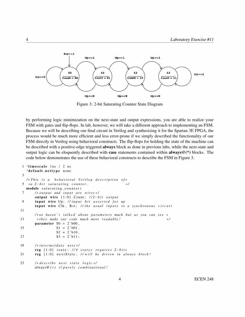
The operation of an FSM can be described with a directed graph such that the vertices represent the statesof the machine and the edges represent the transitions from one state to the next. This sort of graphicalrepresentation of an FSM is known as a state diagram. Figure 3 depicts the state diagram for a 2-bitsaturating counter. If you recall from previous labs, a saturating counter is one that will not roll over butrather, will stop at the minimum or maximum counter value. Let us examine the state diagram and convinceourselves that this is the case.
Each transition or edge of the graph in Figure 3 is marked by are particular input value that causes thattransition. For this simple machine, there is only one input (with the exception of Rst) so we are able toexplicitly represent all input combinations in the diagram. As we will see later on, this is not always thecase. For each vertex, the state is clearly labeled (i.e. S0, S1, S2, and S3); likewise, the output for each statecan be found under the state label. Remember that this is a Moore machine so the outputs are dependentonly on the state of the machine. Given the state diagram of an FSM, the question to be answered now ishow to go from a state diagram to a Verilog description? The next few paragraphs will demonstrate thatexact process.
In lecture, you have learned how to implement an FSM by mapping the design into state tables. Then
ECEN 248 3
4 Laboratory Exercise #11
Figure 3: 2-bit Saturating Counter State Diagram
by performing logic minimization on the next-state and output expressions, you are able to realize yourFSM with gates and flip-flops. In lab, however, we will take a different approach to implementing an FSM.Because we will be describing our final circuit in Verilog and synthesizing it for the Spartan 3E FPGA, theprocess would be much more efficient and less error-prone if we simply described the functionality of ourFSM directly in Verilog using behavioral constructs. The flip-flops for holding the state of the machine canbe described with a positive-edge triggered always block as done in previous labs, while the next-state andoutput logic can be eloquently described with case statements contained within always@(*) blocks. Thecode below demonstrates the use of these behavioral constructs to describe the FSM in Figure 3.
1 ‘ t i m e s c a l e 1 ns / 2 ns‘ d e f a u l t n e t t y p e none
3/∗ T h i s i s a b e h a v i o r a l V e r i l o g d e s c r i p t i o n o f ∗
5 ∗a 2− b i t s a t u r a t i n g c o u n t e r . ∗ /module s a t u r a t i n g c o u n t e r (
7 /∗ o u t p u t and i n p u t are w i r e s ∗ /output wire [ 1 : 0 ] Count ; / / 2− b i t o u t p u t
9 input wire Up ; / / i n p u t b i t a s s e r t e d f o r upinput wire Clk , Rs t ; / / t h e u s u a l i n p u t s t o a s y n c h r o n o u s c i r c u i t
11/∗we haven ’ t t a l k e d abou t p a r a m e t e r s much b u t as you can s e e ∗
13 ∗ t h e y make our code much more r e a d a b l e ! ∗ /parameter S0 = 2 ’ b00 ,
15 S1 = 2 ’ b01 ,S2 = 2 ’ b10 ,
17 S3 = 2 ’ b11 ;
19 /∗ i n t e r m e i d a t e n e t s ∗ /reg [ 1 : 0 ] s t a t e ; / / 4 s t a t e s r e q u i r e s 2− b i t s
21 reg [ 1 : 0 ] n e x t S t a t e ; / / w i l l be d r i v e n i n a lways b l o c k !
23 /∗ d e s c r i b e n e x t s t a t e l o g i c ∗ /always@ ( ∗ ) / / p u r e l y c o m b i n a t i o n a l !
4 ECEN 248

Laboratory Exercise #11 5
25 case ( s t a t e )S0 : begin
27 i f ( Up ) / / c o u n t upn e x t S t a t e = S1 ;
29 e l s e / / s a t u r a t en e x t S t a t e = S0 ;
31 endS1 : begin
33 i f ( Up ) / / c o u n t upn e x t S t a t e = S2 ;
35 e l s e / / c o u n t downn e x t S t a t e = S0 ;
37 endS2 : begin
39 i f ( Up ) / / c o u n t upn e x t S t a t e = S3 ;
41 e l s e / / c o u n t downn e x t S t a t e = S1 ;
43 endS3 : begin
45 i f ( Up ) / / s a t u r a t en e x t S t a t e = S3 ;
47 e l s e / / c o u n t downn e x t S t a t e = S2 ;
49 end/ / do n o t need a d e f a u l t because a l l s t a t e s
51 / / have been t a k e n care o f !endcase
53/∗ d e s c r i b e t h e s y n c h r o n o u s l o g i c t o ho ld our s t a t e ! ∗ /
55 always@ ( posedge Clk )i f ( Rs t ) / / r e s e t s t a t e
57 s t a t e <= S0 ;e l s e
59 s t a t e <= n e x t S t a t e ;
61 /∗ d e s c r i b e t h e o u t p u t l o g i c , which i n t h i s case ∗∗ happens t o j u s t be w i r e s ∗ /
63 a s s i g n Count = s t a t e ;
65 endmodule / / t h a t ’ s i t !
2.3 Rotary Knob and Character LCD on the Spartan 3E
For interacting with the user, we will utilize of the rotary knob and character Liquid Crystal Display (LCD)on the Spartan 3E board. This subsection serves as a high-level introduction to these components. For moreinformation, consult the Spartan 3E User Guide and the Rotary Encoder Interface Guide; however, an in-
ECEN 248 5
6 Laboratory Exercise #11
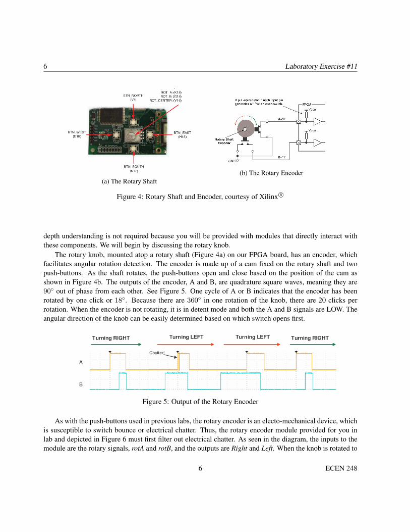
(a) The Rotary Shaft(b) The Rotary Encoder
Figure 4: Rotary Shaft and Encoder, courtesy of Xilinx R©
depth understanding is not required because you will be provided with modules that directly interact withthese components. We will begin by discussing the rotary knob.
The rotary knob, mounted atop a rotary shaft (Figure 4a) on our FPGA board, has an encoder, whichfacilitates angular rotation detection. The encoder is made up of a cam fixed on the rotary shaft and twopush-buttons. As the shaft rotates, the push-buttons open and close based on the position of the cam asshown in Figure 4b. The outputs of the encoder, A and B, are quadrature square waves, meaning they are90◦ out of phase from each other. See Figure 5. One cycle of A or B indicates that the encoder has beenrotated by one click or 18◦. Because there are 360◦ in one rotation of the knob, there are 20 clicks perrotation. When the encoder is not rotating, it is in detent mode and both the A and B signals are LOW. Theangular direction of the knob can be easily determined based on which switch opens first.
Figure 5: Output of the Rotary Encoder
As with the push-buttons used in previous labs, the rotary encoder is an electo-mechanical device, whichis susceptible to switch bounce or electrical chatter. Thus, the rotary encoder module provided for you inlab and depicted in Figure 6 must first filter out electrical chatter. As seen in the diagram, the inputs to themodule are the rotary signals, rotA and rotB, and the outputs are Right and Left. When the knob is rotated to
6 ECEN 248

Laboratory Exercise #11 7
the left, the Left signal will pulse every 18◦. Similarly, when rotated to the right, the Right signal will pulse.To display the angular position of the knob and the status of the combination lock (i.e. locked or
unlocked), we will make use of the 2x16 character LCD on the Spartan 3E board. As illustrated in Figure 6,the LCD driver, which is provided for you, generates the necessary signals to interact with the LCD. Theinterface signals allow the FPGA to communicate ASCII encoded characters to the LCD. We will now takea moment to describe the specific functions of each of these signals.
Figure 6: The Combination-Lock Diagram
The LCD E is an enable signal for the LCD, while the LCD RW indicates whether we are reading orwriting to the memory internal to the LCD. Note that this memory is where the LCD stores 2 rows of 16characters, encoded using ASCII, an 8-bit standard numerical representation of characters. The LCD RSsignal stands for register select and indicates whether the FPGA is sending character data (i.e. ASCIIcodes) or commands. An example command would be “clear display.” Finally, SF D is a 4-bit data bus fortransmitting character data and instructions. Only 4-bits are used as oppose to 8-bits to reduce the numberof I/O pins necessary to communicate with the LCD. Consequently, the FPGA must break each 8-bit codeup into two 4-bit codes and transmit them sequentially. We would like to remind you that the details ofthe LCD interaction will be handled for you in the LCD driver module. The LCD driver module requires aclock, a reset, a 5-bit binary number (0 to 19), and a signal that indicates which mode the combination-lockis in (i.e. locked or unlocked).
3 Pre-lab
The objective of the pre-lab assignment is to describe in Verilog the FSM that you will load onto the Spartan3E board during lab. Therefore, the following subsections will describe the design we are attempting tocreate in detail. The pre-lab deliverables at the end will state what it is you are required to have prior to
ECEN 248 7

8 Laboratory Exercise #11
attending your lab session.
3.1 Digital Combination-Lock
In lab this week, we will design a digital combination-lock that can be used on a safe or access-controlleddoorway. To do so, we will require a few components shown in Figure 6. The rotary encoder module andLCD driver have already been discussed in detail in the background section. Although these two modulesare provided for you, it is imperative that you understand what signals these modules need as input andwhat signals they supply as output. Thus, if you have not already done so, please read over the backgroundsection.
For the remaining two components, you will be responsible for describing them in Verilog. The 0-to-19up/down counter is a simple synchronous circuit that counts up or down in the range of 0 to 19 and rollsover in both directions. In other words, if the Up signal is asserted, the counter will count up until it hits 19,in which case it will roll over to 0. Likewise, when the Down signal is asserted, the counter will count downuntil it hits 0, in which case it will roll over to 19. This counter indicates the position of the rotary knob andmimics the number that the pointer on a combination-lock is pointing to. We will discuss how you would goabout describing this sort of counter in Verilog during the lab session, but for now, try to understand what itis we want it to do.
Figure 7: Rotary Combination-Lock Instructions
The combination-lock FSM is the only component we have not discussed yet. The easiest way to de-scribe the FSM is via a state diagram. However, before delving into the diagram, let us take a high-levellook at how our digital combination-lock is expected to operate. Figure 7 illustrates the steps outline below:
1. Rotate the knob to the right (clockwise) until the number 13 appears on the display.
2. Rotate the knob to the left (counter-clockwise) until the number 7 appears on the display.
3. Rotate the knob to the right again until the number 17 appears on the display.
4. Finally, press the knob (Center button) to unlock the entryway.
5. To lock the entryway, press the South button.
8 ECEN 248
Laboratory Exercise #11 9
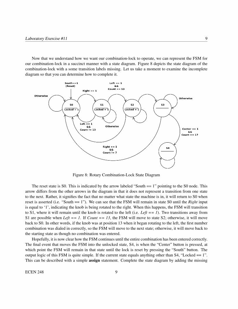
Now that we understand how we want our combination-lock to operate, we can represent the FSM forour combination-lock in a succinct manner with a state diagram. Figure 8 depicts the state diagram of thecombination-lock with a some transition labels missing. Let us take a moment to examine the incompletediagram so that you can determine how to complete it.
Figure 8: Rotary Combination-Lock State Diagram
The reset state is S0. This is indicated by the arrow labeled “South == 1” pointing to the S0 node. Thisarrow differs from the other arrows in the diagram in that it does not represent a transition from one stateto the next. Rather, it signifies the fact that no matter what state the machine is in, it will return to S0 whenreset is asserted (i.e. “South == 1”). We can see that the FSM will remain in state S0 until the Right inputis equal to ‘1’, indicating the knob is being rotated to the right. When this happens, the FSM will transitionto S1, where it will remain until the knob is rotated to the left (i.e. Left == 1). Two transitions away fromS1 are possible when Left == 1. If Count == 13, the FSM will move to state S2; otherwise, it will moveback to S0. In other words, if the knob was at position 13 when it began rotating to the left, the first numbercombination was dialed in correctly, so the FSM will move to the next state; otherwise, it will move back tothe starting state as though no combination was entered.
Hopefully, it is now clear how the FSM continues until the entire combination has been entered correctly.The final event that moves the FSM into the unlocked state, S4, is when the “Center” button is pressed, atwhich point the FSM will remain in that state until the lock is reset by pressing the “South” button. Theoutput logic of this FSM is quite simple. If the current state equals anything other than S4, “Locked == 1”.This can be described with a simple assign statement. Complete the state diagram by adding the missing
ECEN 248 9
10 Laboratory Exercise #11
labels, including the output designations for states S3 and S4.Now that you have a completed the state diagram, use it and the example FSM implementation in the
Background section to describe the combination-lock FSM in behavioral Verilog. The module interfacebelow should get you started. Notice that we are exposing the state nets in the module interface. This is toaide in debugging!/∗ T h i s module d e s c r i b e s t h e combina t ion−l o c k ∗∗FSM d i s c u s s e d i n t h e p r e l a b u s i n g b e h a v i o r a l ∗∗ V e r i l o g ∗ /
module c o m b i n a t i o n l o c k f s m (
/∗ f o r ease o f debugging , o u t p u t s t a t e ∗ /output reg [ 2 : 0 ] s t a t e ,output wire Locked , / / a s s e r t e d when l o c k e dinput wire Right , Le f t , / / i n d i c a t e d i r e c t i o ninput wire [ 4 : 0 ] Count , / / i n d i c a t e p o s i t i o ninput wire Cente r , / / t h e u n l o c k b u t t o ninput wire Clk , South / / c l o c k and r e s e t
) ;
3.2 Pre-lab Deliverables
Include the following items in you pre-lab submission in addition to those items mentioned in the Policiesand Procedures document for this lab course.
1. The completed state diagram for the combination-lock FSM.
2. The combination-lock FSM Verilog module.
4 Lab Procedure
The experiments below will take you through a typical design process in which you describe your design inVerilog, simulated it in ISE, and synthesize it for the Spartan 3E FPGA.
4.1 Experiment 1
The first experiment in lab will involve simulating the combination-lock FSM module you described in thepre-lab to ensure it works properly before attempting to load it on the FPGA board. Additionally, we willcreate a Verilog description of the Up/Down Counter discussed in the pre-lab. As with the combination-lock FSM, we will simulate this module to ensure proper operation prior to integrating it into the top-levelmodule.
1. The following steps will guide you through the process of simulating the FSM that you created in thepre-lab.
10 ECEN 248

Laboratory Exercise #11 11
(a) Create a new ISE project called “lab11” and add your combination-lock FSM module to thatproject.
(b) Copy the test bench file, “combination lock fsm tb.v”, from the course directory into yourlab11 directory.
(c) Add the test bench file you just copied over to your ISE project and simulate its operation.
(d) Examine the console output of the test bench and ensure all of the tests passed.
(e) Likewise, take a look at the simulation waveform and take note of the tests that the test benchperforms. Is this an exhaustive test? Why or why not?
2. The last component that we must describe in Verilog before we can begin creating our top-level mod-ule is the 0-to-19, Up/Down Counter, which will keep track of the position of our rotary knob. Obvi-ously, what is unique about this counter is that its maximum value is not a power-of-two. Althoughthe gate-level design may be significantly more involved than that of a traditional counter, behavioralVerilog does a good job of hiding the complexity. Therefore, behavioral Verilog is what we will useto create this counter! The steps below will take you through the development and simulation of thismodule.
(a) Type the code below into a file called “up down counter.v”.
‘ t i m e s c a l e 1 ns / 1 ps2 ‘ d e f a u l t n e t t y p e none
4 /∗ T h i s b e h a v i o r a l V e r i l o g d e s c r i p t i o n models ∗∗an up down c o u n t e r t h a t c o u n t s be tween 0−19∗ /
6 module u p d o w n c o u n t e r (/∗ o u t p u t w i l l be d r i v e n i n an a lways b l o c k ∗ /
8 output reg [ 4 : 0 ] Count ,input wire Up , Down ,
10 input wire Clk , South) ;
12/∗ p o s i t i v e edge t r i g g e r e d s y n c h r o n o u s l o g i c ∗
14 /∗ w i t h a s y n c h r o n o u s r e s e t ∗ /always@ ( posedge Clk )
16 i f ( South )Count <= 0 ;
18 e l s e i f ( Up )begin
20 i f ( Count == 19) / / i f a t t o p endCount <= 0 ; / / r o l l ove r
22 e l s e / / c o u n t upCount <= Count + 1 ;
24 ende l s e i f (Down)
26 / / now do s o m e t h i n g s i m i l a r f o r
ECEN 248 11

12 Laboratory Exercise #11
/ / down c o u n t i n g . . .28
30
32 endmodule
(b) Now fill in the missing pieces and add the source file to your ISE project.
(c) Copy the test bench file, “up down counter tb.v”, from the course directory into your lab11 di-rectory.
(d) Add the test bench file you just copied over to your ISE project and simulate its operation.
(e) Examine the console output of the test bench and ensure all of the tests passed.
(f) Likewise, take a look at the simulation waveform and make a note in your lab write-up abouthow the test bench tests the operation of your Up/Down Counter.
4.2 Experiment 2
For the final experiment, you will integrate the modules you simulated in the previous experiment with therotary encoder and the LCD driver modules into a top-level module. You will then synthesize and implementthe top-level module and load it onto the FPGA.
1. Synthesize and implement the combination-lock top-level module with the following steps:
(a) Copy over the following files from the course directory into you lab10 directory:
• “rotary combination lock.v”, the top-level Verilog module• “rotary combination lock.ucf”, the UCF for the top-level• “synchronizer.v”, the synchronizer module for our asynchronous inputs• “lcd driver.v”, the driver module for the character LCD screen• “rotary encoder module.v”, the quadrature decoding module
(b) Add the aforementioned files along with your combination-lock FSM module and Up/DownCounter module to your ISE project.
(c) Set the rotary combination lock module as the top-level module and kick off the synthesisprocess. Correct any errors with your design.
(d) Once your design builds without errors and warnings, load it onto the FPGA board.
2. With the combination-lock design loaded onto the FPGA, test its operation.
(a) Press the “South” button on the Spartan 3E board. You should see the following on the LCDscreen:
>00 LOCKED
12 ECEN 248

Laboratory Exercise #11 13
If you do not see this pattern of characters on the screen, you will need to begin debugging yourdesign.Hint: Because we simulated the operation of the individual components, the problem is likelyin the implementation phase. For example, you may have forgot to add the UCF file to yourproject.
(b) With the correct output on the LCD screen, run through the combination sequence shown in thepre-lab with the rotary knob. The LCD screen will display “UNLOCKED” when the correctcombination has been entered. Ensure the design operates as expected. If it does not, you maywant to connect the logic analyzer up to J1 and walk through the state transitions of your design.Note: When your design works properly, demonstrate your progress to the TA.
3. At this point, we have demonstrated our prototype to our customer, and they liked what they saw.However, they mentioned that they would like to use the lock to secure sensitive company informationand would require a more secure combination. Thus, we will modify our existing design to accept afour number combination instead of just three.
(a) Modify the Verilog source to require the input of a fourth number of your choosing in the com-bination. This will require the addition of one more state in your FSM.
(b) Re-synthesize and implement your design in ISE.
(c) Load the design on the FPGA and ensure that it works properly. As with the previous test, youmay want to use the logic analyzer to aide in debugging. Note: When your modifications workproperly, demonstrate your progress to the TA.
5 Post-lab Deliverables
Please include the following items in your post-lab write-up in addition to the deliverables mentioned in thePolicies and Procedures document.
1. Include the source code with comments for all modules you simulated and/or implemented in lab.You do not have to include test bench code that was provided! Code without comments will not beaccepted!
2. Include screenshots of all waveforms captured during simulation in addition to the test bench consoleoutput for each test bench simulation.
3. Answer all questions throughout the lab manual.
4. A possible attack on your combination-lock is a brute-force attack in which every possible inputcombination is tried. Given the original design with a combination of three numbers between 0 and 19,how many possible input combinations exist? How about for the modified design with a combinationof four numbers?
ECEN 248 13

14 Laboratory Exercise #11
6 Important Student Feedback
The last part of lab requests your feedback. We are continually trying to improve the laboratory exercisesto enhance your learning experience, and we are unable to do so without your feedback. Please include thefollowing post-lab deliverables in your lab write-up.Note: If you have any other comments regarding the lab that you wish to bring to your instructor’s attention,please feel free to include them as well.
1. What did you like most about the lab assignment and why? What did you like least about it and why?
2. Were there any section of the lab manual that were unclear? If so, what was unclear? Do you haveany suggestions for improving the clarity?
3. What suggestions do you have to improve the overall lab assignment?
14 ECEN 248