lab 1: introductory experiments and linear circuits icaug/111/lab-1-introductory.pdf · lab 1:...
TRANSCRIPT
Lab 1: Introductory Experiments and Linear Circuits I
Christopher AgostinoLab Partner: MacCallum Robertson
February 19, 2015
Introduction
In this lab, we intend to learn how to properly use the equipment that we will use in this course and inany setting where understanding and debugging circuits are essential skills. In addition to this, we seekto learn about linear circuits which comprise some of the simplest circuits we can create. A masteryof linear circuits, their components, such as resistors, capacitors, etc. and various measuring tools isnecessary for understanding and debugging more complex circuits. Specifically we will learn the basicsof breadboards, Digital Multimeters, an Oscilloscopes, function generators, and power supplies. Wewill be introduced to the concepts of complex impedance, the generalized Ohm’s Law, voltage dividers,Thevenin equivalent resistance and voltage. We will try to distinguish the differences between AC andDC signals and their associated properties and figure out the best ways to measure their properties suchas the peak voltage and the root mean square voltage. We will also begin to combine resistors andcapacitors to make useful devices such as filters.
1 Lab Exercises: Part I
1.1
Breadboards often have two rails along the side of them separated from the rest of the board. Theserails are typically where voltages are connected and floated along the rails, horizontally in our picture,whereas on the rest of the breadboard any connection is made perpendicularly along each separate row.
Figure 1: Breadboard connections. Source: Lab manual
1.2
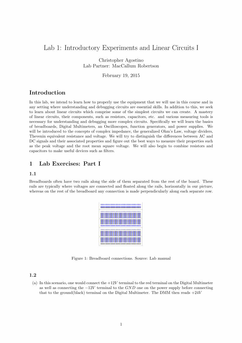
(a) In this scenario, one would connect the +12V terminal to the red terminal on the Digital Multimeteras well as connecting the −12V terminal to the GND one on the power supply before connectingthat to the ground(black) terminal on the Digital Multimeter. The DMM then reads +24V
1
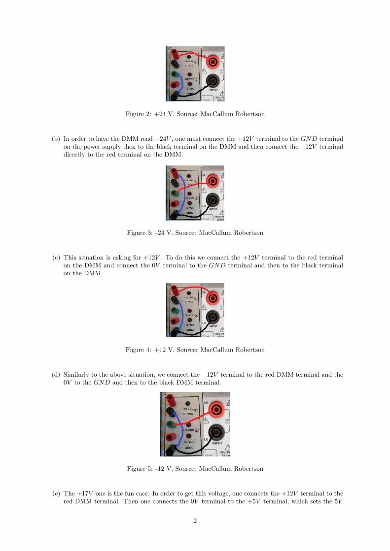
Figure 2: +24 V. Source: MacCallum Robertson
(b) In order to have the DMM read −24V , one must connect the +12V terminal to the GND terminalon the power supply then to the black terminal on the DMM and then connect the −12V terminaldirectly to the red terminal on the DMM.
Figure 3: -24 V. Source: MacCallum Robertson
(c) This situation is asking for +12V . To do this we connect the +12V terminal to the red terminalon the DMM and connect the 0V terminal to the GND terminal and then to the black terminalon the DMM.
Figure 4: +12 V. Source: MacCallum Robertson
(d) Similarly to the above situation, we connect the −12V terminal to the red DMM terminal and the0V to the GND and then to the black DMM terminal.
Figure 5: -12 V. Source: MacCallum Robertson
(e) The +17V one is the fun case. In order to get this voltage, one connects the +12V terminal to thered DMM terminal. Then one connects the 0V terminal to the +5V terminal, which sets the 5V
2

as the common point in the float supply so the +12V is now 12V relative to 5V , making it 17V .We are not done there yet, we must also connect the GND terminal to the black terminal on theDMM to complete the circuit.
Figure 6: +17 V. Source: MacCallum Robertson
1.3
If one were to try to measure the potential between the +12V output and the 5V supply ground, onewould measure 0V because the 12V supply is a floating power supply so it is not electrically connectedto ground whereas the 5V supply is relative to ground. The 12V is not relative to the ground supply soit would not make any sense to try to measure the difference between it and the 5V supply.
1.4 1.1.4
In order to derive the voltage divider equation for the voltage divider present in figure 7, we start withOhm’s law, V = IR.
Figure 7: Voltage Divider
We note that Rtot = R1 + R2 and by charge conservation in this series resistor circuit, the currentthrough each resistor has to be the same. By Kirchoff’s Law the voltage drop through the entire circuithas to be equal to Vin. Thus we can set up this system of equations and recognize that Vout must beequal to the voltage drop across only the second resistor.
Vin = I(R1 +R2)
Vout = I(R2)
We solve each for I then set them equal to each other and find that
I =Vin
R1 +R2=VoutR2
which yields the final result by solving in terms of Vout to be
Vout = VinR2
R1 +R2
1.5 1.1.5
Here we are looking to find the current in our circuit given that R2 is 470kΩ and R1 is 10kΩ. We takeVin to be 24V and solve accordingly using our relationships derived in 1.1.4
I =24V
480kΩ= 5.0 ∗ 10−5A
3
1.6 1.1.6
Here we are solving for Vout. We use our equation derived in 1.1.4 given our resistor and voltage values.
Vout = Vin ∗R2
R2 +R1= 24V ∗ 470kΩ
480kΩ= 23.5V
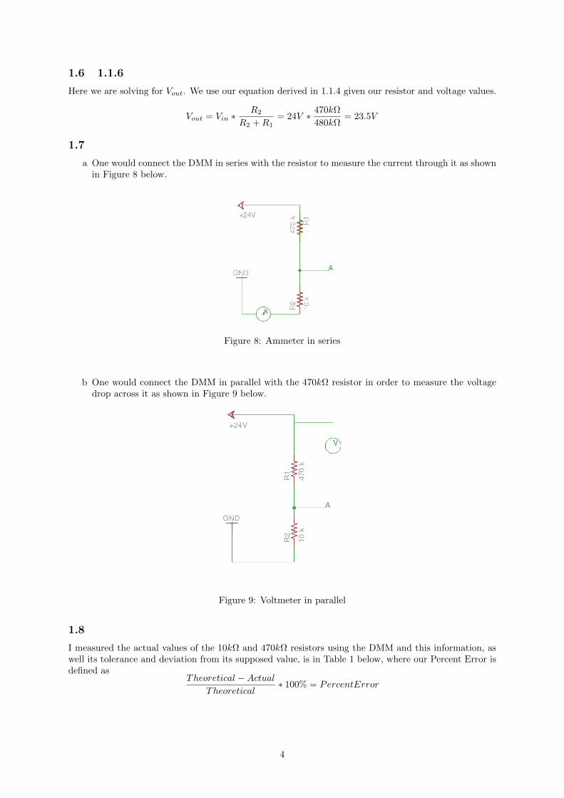
1.7
a One would connect the DMM in series with the resistor to measure the current through it as shownin Figure 8 below.
Figure 8: Ammeter in series
b One would connect the DMM in parallel with the 470kΩ resistor in order to measure the voltagedrop across it as shown in Figure 9 below.
Figure 9: Voltmeter in parallel
1.8
I measured the actual values of the 10kΩ and 470kΩ resistors using the DMM and this information, aswell its tolerance and deviation from its supposed value, is in Table 1 below, where our Percent Error isdefined as
Theoretical −ActualTheoretical
∗ 100% = PercentError
4
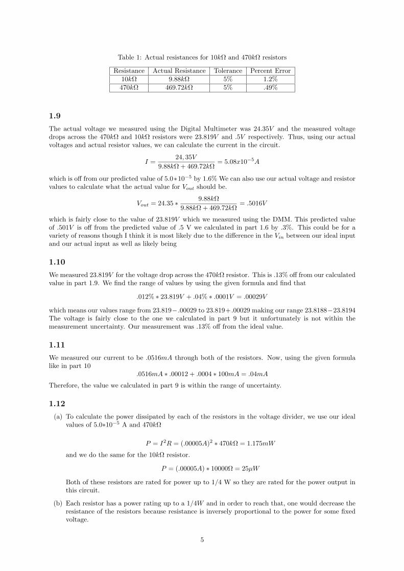
Table 1: Actual resistances for 10kΩ and 470kΩ resistors
Resistance Actual Resistance Tolerance Percent Error10kΩ 9.88kΩ 5% 1.2%470kΩ 469.72kΩ 5% .49%
1.9
The actual voltage we measured using the Digital Multimeter was 24.35V and the measured voltagedrops across the 470kΩ and 10kΩ resistors were 23.819V and .5V respectively. Thus, using our actualvoltages and actual resistor values, we can calculate the current in the circuit.
I =24, 35V
9.88kΩ + 469.72kΩ= 5.08x10⁻⁵A
which is off from our predicted value of 5.0∗10−5 by 1.6% We can also use our actual voltage and resistorvalues to calculate what the actual value for Vout should be.
Vout = 24.35 ∗ 9.88kΩ
9.88kΩ + 469.72kΩ= .5016V
which is fairly close to the value of 23.819V which we measured using the DMM. This predicted valueof .501V is off from the predicted value of .5 V we calculated in part 1.6 by .3%. This could be for avariety of reasons though I think it is most likely due to the difference in the Vin between our ideal inputand our actual input as well as likely being
1.10
We measured 23.819V for the voltage drop across the 470kΩ resistor. This is .13% off from our calculatedvalue in part 1.9. We find the range of values by using the given formula and find that
.012% ∗ 23.819V + .04% ∗ .0001V = .00029V
which means our values range from 23.819−.00029 to 23.819+.00029 making our range 23.8188−23.8194The voltage is fairly close to the one we calculated in part 9 but it unfortunately is not within themeasurement uncertainty. Our measurement was .13% off from the ideal value.
1.11
We measured our current to be .0516mA through both of the resistors. Now, using the given formulalike in part 10
.0516mA ∗ .00012 + .0004 ∗ 100mA = .04mA
Therefore, the value we calculated in part 9 is within the range of uncertainty.
1.12
(a) To calculate the power dissipated by each of the resistors in the voltage divider, we use our idealvalues of 5.0∗10−5 A and 470kΩ
P = I2R = (.00005A)2 ∗ 470kΩ = 1.175mW
and we do the same for the 10kΩ resistor.
P = (.00005A) ∗ 10000Ω = 25µW
Both of these resistors are rated for power up to 1/4 W so they are rated for the power output inthis circuit.
(b) Each resistor has a power rating up to a 1/4W and in order to reach that, one would decrease theresistance of the resistors because resistance is inversely proportional to the power for some fixedvoltage.
5
(c) The 470kΩ resistor would reach its max power rating first because it has a higher resistance.
(d) In order to find the max value for one of the two resistors to exceed its power rating, we mustcalculate the resistor value at which a 24V signal would generate .25W .
.25W =242V 2
xΩ→ x = 576V 2/.25W = 2304Ω
Now this is not a resistance one is likely to encounter in any real situation so I will assume a valueof 2.2kΩ as it is the closest common value. Now we can use our ratio to calculate the other resistorvalue we would need.
x
2.2kΩ=
470000kΩ
10000kΩ→ x = 103400Ω ≈ 100kΩ
So in order to do this, you would need to make both resistors smaller by a factor of about 4.5
(e) This would not be very easily accomplished in the lab as these resistances do not match thosefound in common resistors. It would, however, be easy to do something quite similar with 2.2k and100k resistors.
1.13
When trying to find the signal on the scope after the settings have been messed with, it is important tocheck the V/div, the vertical position, the time scale, and whether or not it is AC coupled, DC input,or set to ground. It could also be the case that the scope is in XY mode in which case you would simplyturn off XY mode to get back to the normal input. In addition, it is wise to check whether or not thechannel you are trying to measure a signal on is actually turned on. Otherwise, there aren’t that manymore commonly used settings on the oscilloscope, or at least settings which will be applicable in thiscourse.
1.14
We generated the triangular wave by hitting the Ramp button the function generator. We then generateda sawtooth like wave by adjusting the the output parameters on the initial ramp wave. Then we generatedthe pulsed squares by using the pulse option and adjusting the width of the pulse output and the frequencyof the signal to have three waveforms appear on the scope screen.
1.17
(a) We connected the 5V power supply to the DMM in the 10V range and measured the actual voltageto be 5.0565V . Thus we can calculate the range using the same formula we used in 1.10 and 1.11
.00012 ∗ 5.0565V + .0004 ∗ .1mV = .0061V
Therefore we can write the voltage measurement as being 5.0565± .00061V .
(b) We then connected the 5V power supply to the Oscilloscope and measured the voltage to be 5.10V .The range was 200 mV on the scope so we can calculate the uncertainty.
.00012 ∗ 5.10V + .0004 ∗ .2V = 6.92 ∗ 10−4V
which allows to write the voltage measurement as 5.10V ± 6.92 ∗ 10−4V
(c) We then altered the settings on the scope and remeasured the voltage. Using the range of 2V/div(.4 V/tick), we found that the Oscilloscope measured 5.04 V using channel one. When we pluggedthe same signal in to channel 2, we also measured 5.04 V at 2V/div. We can find the uncertaintyof this measurement to be
5.04V ∗ .00012 + .0004 ∗ .4V = 7.65 ∗ 10−4V
giving us a range of 5.04V ± 7.65 ∗ 10−4. The measurements by the DMM and scope with dif-ferent settings are not consistent with each other within the calculated uncertainty and measureslightly different values for the voltage which is likely due to the two devices having different inputimpedances
6
(d) For this setup, the scope should be set up such that the zero of the scope is at the bottom of thegraph and the V/div should be as small as possible such that the highest point of the signal is stillon the screen.
1.18
(a) We had the scope connected to the 5 volt supply and turned on the A.C. coupling. This settingignores the DC offset voltage and only displays voltages associated with the alternating currentpart of the signal.
(b) When you look closer at the A.C. part of the signal, one begins to notice that there is no real clearpattern in the signals displayed on the scope. It has a kind of random wave for which oscillatesaround 0 V. Essentially,we are seeing the electrical noise from the power supply, which senselesslyvaries among low voltages around 0 V.
1.19
(a) For a voltage varying sinusoidally, we have some basic form for the voltage V (θ) = Vpeaksin(θ)where Vpeak is the amplitude. We choose to calculate the root-mean-square voltage over the firstquarter of the period as it is symmetric to the other parts.
Vrms =
√1
π/2
∫ π/2
0
(Vpeak ∗ sin(θ))2dθ
We can rewrite sin2(θ) using our double angle identity and then we can evaluate the integral to be
vrms =
√2 ∗ Vpeak√
π
√θ/2− 1/4sin(2θ)
evaluated at the limits of 0 and π/2
Vrms =
√2√π∗ Vpeak ∗
√(π/4− 0)− (0− 0) = Vmax ∗
√2/2 =
Vmax√2
(b) Now we look at the triangular wave. Similarly, we go over a quarter of the cycle for simplicity andbecause of symmetry. For the first quarter we can write the voltage as a function of time beingV (t) = Vpeak ∗ t ∗ 4/P where the 4/P comes in as the function reaches Vmax at time t = P/4. Wethen begin a similar analysis to find the root-mean-square voltage of the triangle wave.
Vrms =
√1
P/4
∫ P/4
0
(Vpeak4t/P )2dt =
√(
4
P)3V 2
peak
∫ P/4
0
t2dt
The integral evaluates to t3/3 evaluated at the limits 0 and P/4 which gets rid of the (4/P )3 termand introduces a 1/3 term which at the end evaluates to
Vrms =Vpeak√
3
(c) For square waves, the root-mean-square voltage is equal to its peak voltage because there is novariation over symmetrical parts of the waveform. The voltage is either equal to −Vpeak or +Vpeakand when squared it eliminates the possible for any variation such that
Vrms = Vpeak
We then fed in 1Vpeak sine, triangle, and square waves at 1 kHz into the DMM and measured theVrms for each type of wave and found that the RMS voltages we measured were convincingly closeto the values predicted by the coefficients we derived in this problem.
7
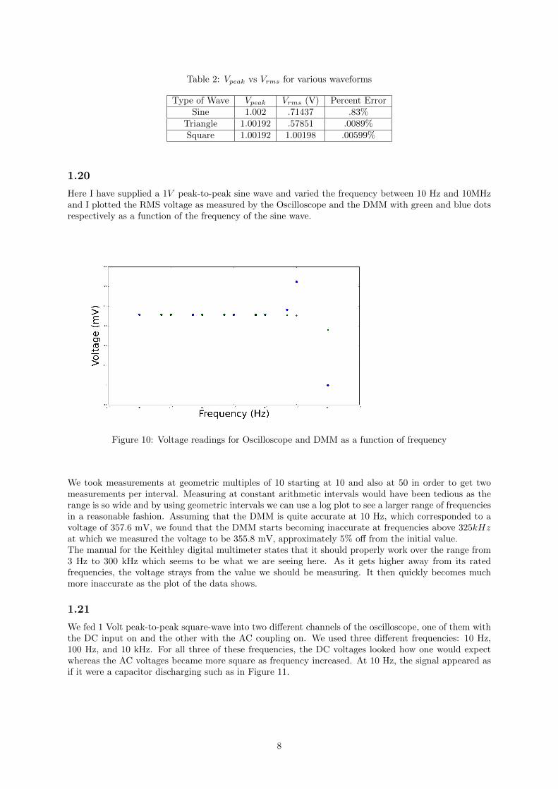
Table 2: Vpeak vs Vrms for various waveforms
Type of Wave Vpeak Vrms (V) Percent ErrorSine 1.002 .71437 .83%
Triangle 1.00192 .57851 .0089%Square 1.00192 1.00198 .00599%
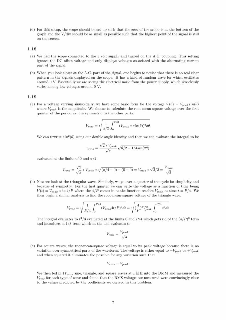
1.20
Here I have supplied a 1V peak-to-peak sine wave and varied the frequency between 10 Hz and 10MHzand I plotted the RMS voltage as measured by the Oscilloscope and the DMM with green and blue dotsrespectively as a function of the frequency of the sine wave.
Figure 10: Voltage readings for Oscilloscope and DMM as a function of frequency
We took measurements at geometric multiples of 10 starting at 10 and also at 50 in order to get twomeasurements per interval. Measuring at constant arithmetic intervals would have been tedious as therange is so wide and by using geometric intervals we can use a log plot to see a larger range of frequenciesin a reasonable fashion. Assuming that the DMM is quite accurate at 10 Hz, which corresponded to avoltage of 357.6 mV, we found that the DMM starts becoming inaccurate at frequencies above 325kHzat which we measured the voltage to be 355.8 mV, approximately 5% off from the initial value.The manual for the Keithley digital multimeter states that it should properly work over the range from3 Hz to 300 kHz which seems to be what we are seeing here. As it gets higher away from its ratedfrequencies, the voltage strays from the value we should be measuring. It then quickly becomes muchmore inaccurate as the plot of the data shows.
1.21
We fed 1 Volt peak-to-peak square-wave into two different channels of the oscilloscope, one of them withthe DC input on and the other with the AC coupling on. We used three different frequencies: 10 Hz,100 Hz, and 10 kHz. For all three of these frequencies, the DC voltages looked how one would expectwhereas the AC voltages became more square as frequency increased. At 10 Hz, the signal appeared asif it were a capacitor discharging such as in Figure 11.
8
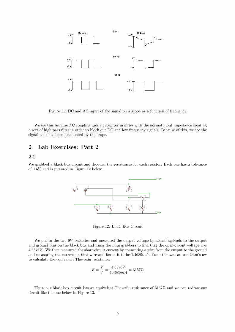
Figure 11: DC and AC input of the signal on a scope as a function of frequency
We see this because AC coupling uses a capacitor in series with the normal input impedance creatinga sort of high pass filter in order to block out DC and low frequency signals. Because of this, we see thesignal as it has been attenuated by the scope.
2 Lab Exercises: Part 2
2.1
We grabbed a black box circuit and decoded the resistances for each resistor. Each one has a toleranceof ±5% and is pictured in Figure 12 below.
Figure 12: Black Box Circuit
We put in the two 9V batteries and measured the output voltage by attaching leads to the outputand ground pins on the black box and using the mini grabbers to find that the open-circuit voltage was4.6376V . We then measured the short-circuit current by connecting a wire from the output to the groundand measuring the current on that wire and found it to be 1.4689mA. From this we can use Ohm’s awto calculate the equivalent Thevenin resistance.
R =V
I=
4.6376V
1.4689mA= 3157Ω
Thus, our black box circuit has an equivalent Thevenin resistance of 3157Ω and we can redraw ourcircuit like the one below in Figure 13.
9
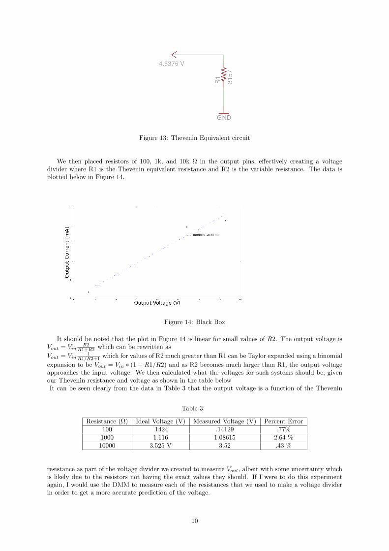
Figure 13: Thevenin Equivalent circuit
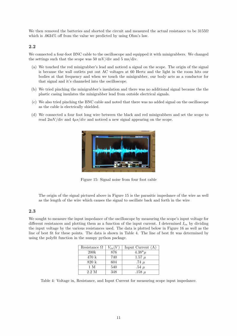
We then placed resistors of 100, 1k, and 10k Ω in the output pins, effectively creating a voltagedivider where R1 is the Thevenin equivalent resistance and R2 is the variable resistance. The data isplotted below in Figure 14.
Figure 14: Black Box
It should be noted that the plot in Figure 14 is linear for small values of R2. The output voltage isVout = Vin
R2R1+R2 which can be rewritten as
Vout = Vin1
R1/R2+1 which for values of R2 much greater than R1 can be Taylor expanded using a binomial
expansion to be Vout = Vin ∗ (1− R1/R2) and as R2 becomes much larger than R1, the output voltageapproaches the input voltage. We then calculated what the voltages for such systems should be, givenour Thevenin resistance and voltage as shown in the table belowIt can be seen clearly from the data in Table 3 that the output voltage is a function of the Thevenin
Table 3:
Resistance (Ω) Ideal Voltage (V) Measured Voltage (V) Percent Error100 .1424 .14129 .77%1000 1.116 1.08615 2.64 %10000 3.525 V 3.52 .43 %
resistance as part of the voltage divider we created to measure Vout, albeit with some uncertainty whichis likely due to the resistors not having the exact values they should. If I were to do this experimentagain, I would use the DMM to measure each of the resistances that we used to make a voltage dividerin order to get a more accurate prediction of the voltage.
10
We then removed the batteries and shorted the circuit and measured the actual resistance to be 3155Ωwhich is .0634% off from the value we predicted by using Ohm’s law.
2.2
We connected a four-foot BNC cable to the oscilloscope and equipped it with minigrabbers. We changedthe settings such that the scope was 50 mV/div and 5 ms/div.
(a) We touched the red minigrabber’s lead and noticed a signal on the scope. The origin of the signalis because the wall outlets put out AC voltages at 60 Hertz and the light in the room hits ourbodies at that frequency and when we touch the minigrabber, our body acts as a conductor forthat signal and it’s channeled into the oscilloscope.
(b) We tried pinching the minigrabber’s insulation and there was no additional signal because the theplastic casing insulates the minigrabber lead from outside electrical signals.
(c) We also tried pinching the BNC cable and noted that there was no added signal on the oscilloscopeas the cable is electrically shielded.
(d) We connected a four foot long wire between the black and red minigrabbers and set the scope toread 2mV/div and 4µs/div and noticed a new signal appearing on the scope.
Figure 15: Signal noise from four foot cable
The origin of the signal pictured above in Figure 15 is the parasitic impedance of the wire as wellas the length of the wire which causes the signal to oscillate back and forth in the wire
2.3
We sought to measure the input impedance of the oscilloscope by measuring the scope’s input voltage fordifferent resistances and plotting them as a function of the input current. I determined Iin by dividingthe input voltage by the various resistances used. The data is plotted below in Figure 16 as well as theline of best fit for these points. The data is shown in Table 4. The line of best fit was determined byusing the polyfit function in the numpy python package.
Resistance Ω Vin(V ) Input Current (A)200k 876 4.38*µ470 k 740 1.57 µ820 k 604 .74 µ1 M 540 .54 µ
2.2 M 348 .158 µ
Table 4: Voltage in, Resistance, and Input Current for measuring scope input impedance.
11
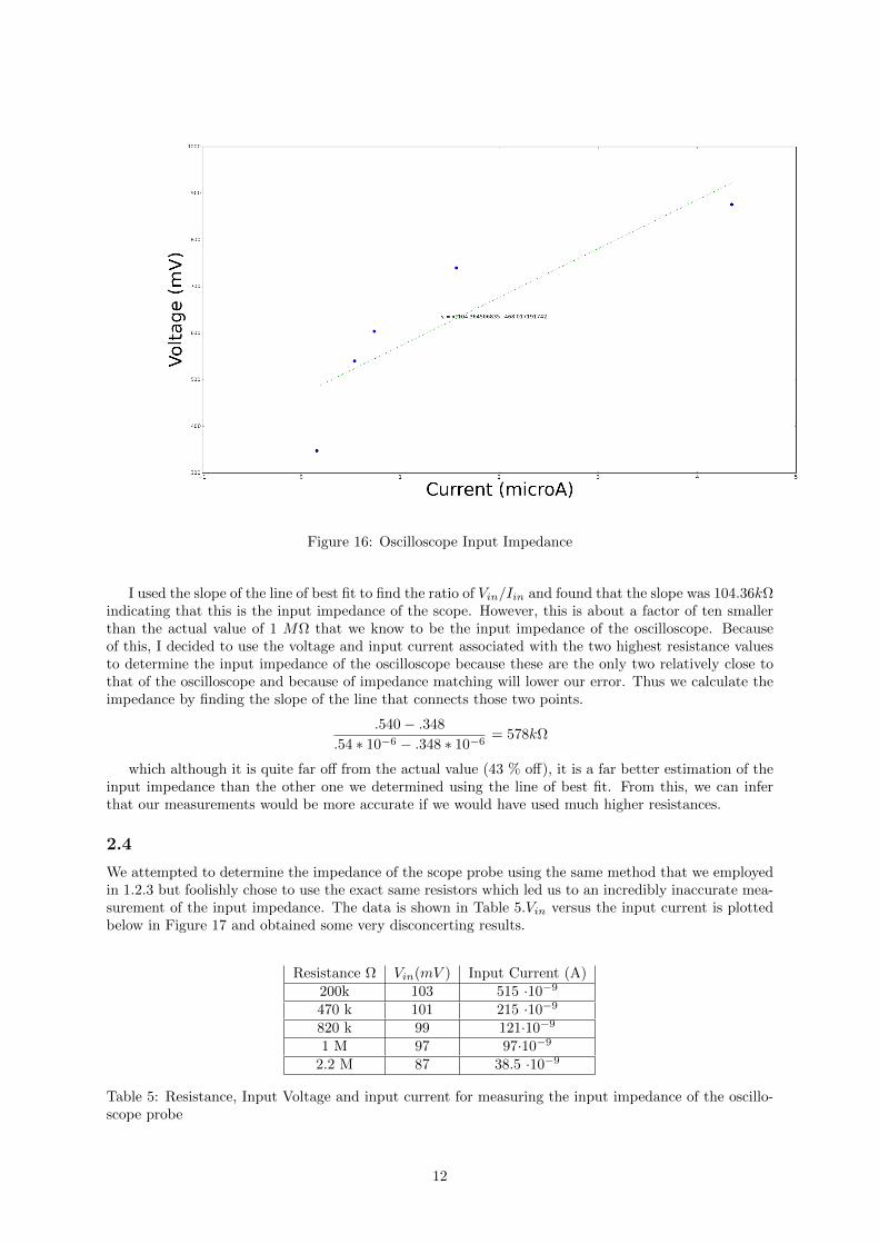
Figure 16: Oscilloscope Input Impedance
I used the slope of the line of best fit to find the ratio of Vin/Iin and found that the slope was 104.36kΩindicating that this is the input impedance of the scope. However, this is about a factor of ten smallerthan the actual value of 1 MΩ that we know to be the input impedance of the oscilloscope. Becauseof this, I decided to use the voltage and input current associated with the two highest resistance valuesto determine the input impedance of the oscilloscope because these are the only two relatively close tothat of the oscilloscope and because of impedance matching will lower our error. Thus we calculate theimpedance by finding the slope of the line that connects those two points.
.540− .348
.54 ∗ 10−6 − .348 ∗ 10−6= 578kΩ
which although it is quite far off from the actual value (43 % off), it is a far better estimation of theinput impedance than the other one we determined using the line of best fit. From this, we can inferthat our measurements would be more accurate if we would have used much higher resistances.
2.4
We attempted to determine the impedance of the scope probe using the same method that we employedin 1.2.3 but foolishly chose to use the exact same resistors which led us to an incredibly inaccurate mea-surement of the input impedance. The data is shown in Table 5.Vin versus the input current is plottedbelow in Figure 17 and obtained some very disconcerting results.
Resistance Ω Vin(mV ) Input Current (A)200k 103 515 ·10−9
470 k 101 215 ·10−9
820 k 99 121·10−9
1 M 97 97·10−9
2.2 M 87 38.5 ·10−9
Table 5: Resistance, Input Voltage and input current for measuring the input impedance of the oscillo-scope probe
12
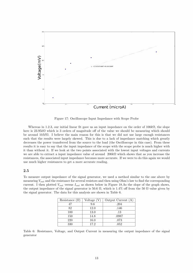
Figure 17: Oscilloscope Input Impedance with Scope Probe
Whereas in 1.2.3, our initial linear fit gave us an input impedance on the order of 100kΩ, the slopehere is 23.95kΩ which is 3 orders of magnitude off of the value we should be measuring which shouldbe around 10MΩ. I believe the main reason for this is that we did not use large enough resistancessuch that the results were largely skewed. This is due to a lack of impedance matching which greatlydecreases the power transferred from the source to the load (the Oscilloscope in this case). From theseresults it is easy to say that the input impedance of the scope with the scope probe is much higher withit than without it. If we look at the two points associated with the lowest input voltages and currentswe are able to extract a input impedance value of around 200kΩ which shows that as you increase theresistances, the associated input impedance becomes more accurate. If we were to do this again we woulduse much higher resistances to get a more accurate reading.
2.5
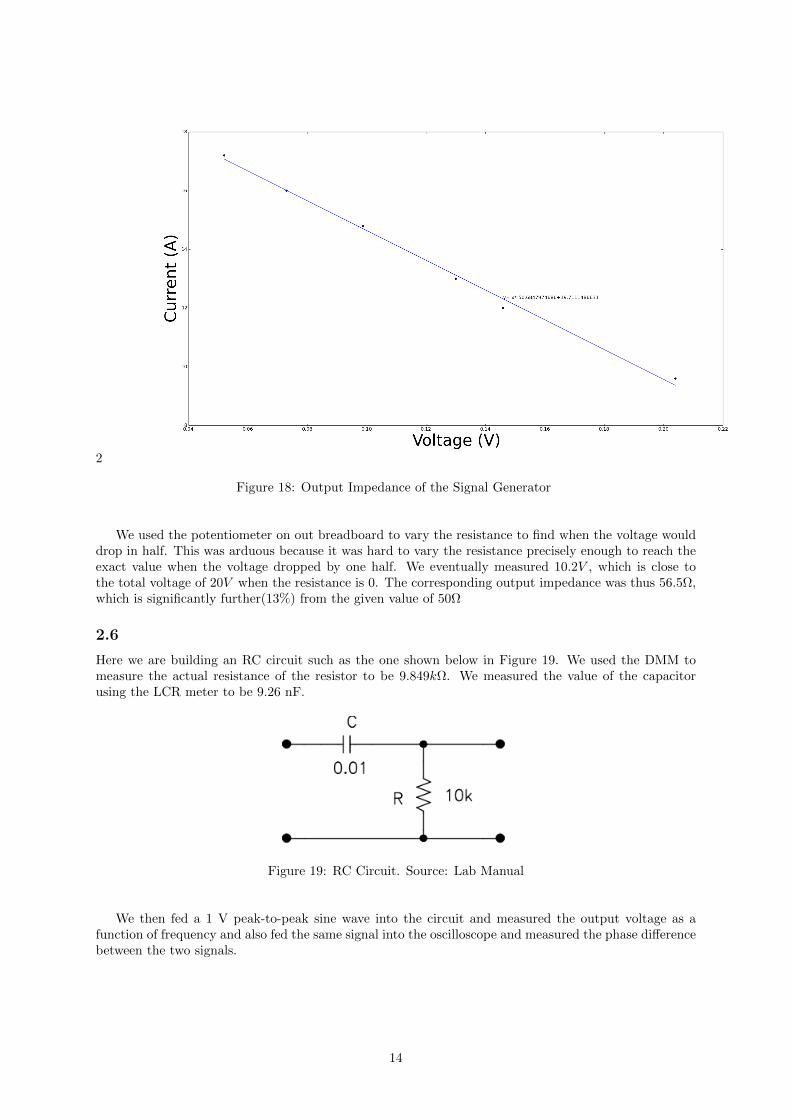
To measure output impedance of the signal generator, we used a method similar to the one above bymeasuring Vout and the resistance for several resistors and then using Ohm’s law to find the correspondingcurrent. I then plotted Vout versus Iout as shown below in Figure 18.As the slope of the graph shows,the output impedance of the signal generator is 50.6 Ω, which is 1.4% off from the 50 Ω value given bythe signal generator. The data for this analysis are shown in Table 6.
Resistance (Ω) Voltage (V) Output Current (A)47 9.6 .20482 12.0 .146100 13.0 .13150 14.8 .0987220 16.0 .073330 17.2 .052
Table 6: Resistance, Voltage, and Output Current in measuring the output impedance of the signalgenerator
13
2
Figure 18: Output Impedance of the Signal Generator
We used the potentiometer on out breadboard to vary the resistance to find when the voltage woulddrop in half. This was arduous because it was hard to vary the resistance precisely enough to reach theexact value when the voltage dropped by one half. We eventually measured 10.2V , which is close tothe total voltage of 20V when the resistance is 0. The corresponding output impedance was thus 56.5Ω,which is significantly further(13%) from the given value of 50Ω
2.6
Here we are building an RC circuit such as the one shown below in Figure 19. We used the DMM tomeasure the actual resistance of the resistor to be 9.849kΩ. We measured the value of the capacitorusing the LCR meter to be 9.26 nF.
Figure 19: RC Circuit. Source: Lab Manual
We then fed a 1 V peak-to-peak sine wave into the circuit and measured the output voltage as afunction of frequency and also fed the same signal into the oscilloscope and measured the phase differencebetween the two signals.
14
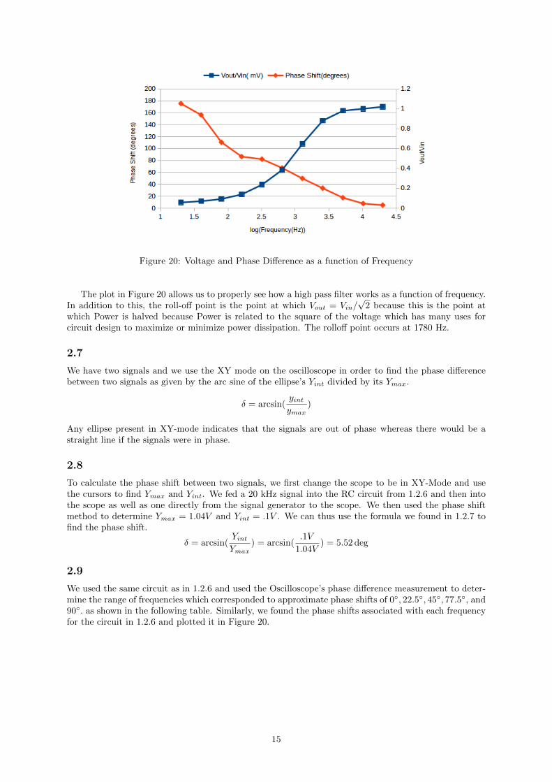
Figure 20: Voltage and Phase Difference as a function of Frequency
The plot in Figure 20 allows us to properly see how a high pass filter works as a function of frequency.In addition to this, the roll-off point is the point at which Vout = Vin/
√2 because this is the point at
which Power is halved because Power is related to the square of the voltage which has many uses forcircuit design to maximize or minimize power dissipation. The rolloff point occurs at 1780 Hz.
2.7
We have two signals and we use the XY mode on the oscilloscope in order to find the phase differencebetween two signals as given by the arc sine of the ellipse’s Yint divided by its Ymax.
δ = arcsin(yintymax
)
Any ellipse present in XY-mode indicates that the signals are out of phase whereas there would be astraight line if the signals were in phase.
2.8
To calculate the phase shift between two signals, we first change the scope to be in XY-Mode and usethe cursors to find Ymax and Yint. We fed a 20 kHz signal into the RC circuit from 1.2.6 and then intothe scope as well as one directly from the signal generator to the scope. We then used the phase shiftmethod to determine Ymax = 1.04V and Yint = .1V . We can thus use the formula we found in 1.2.7 tofind the phase shift.
δ = arcsin(YintYmax
) = arcsin(.1V
1.04V) = 5.52 deg
2.9
We used the same circuit as in 1.2.6 and used the Oscilloscope’s phase difference measurement to deter-mine the range of frequencies which corresponded to approximate phase shifts of 0, 22.5, 45, 77.5, and90. as shown in the following table. Similarly, we found the phase shifts associated with each frequencyfor the circuit in 1.2.6 and plotted it in Figure 20.
15
Phase Shift Frequency Range0 500 kHz - 2 MHz
22.5 3.8 kHz - 4.2 kHz45 1.6 kHz -1.7 kHz
77.5 190 Hz-250 Hz
Table 7: Ranges of frequency for certain phase shifts for the RC circuit in 2.6
2.10
We have here that the output voltage of a black-box decreases by 20% with a load of 1kΩ compared tothe no-load output. Thus we know that Vnoload = VThevenin and that Vload = .8VThevenin. Similarly,Inoload = 0 and Iload = .8 ∗ VThevenin/R2 where R2 is the 1kΩ resistor. We also know from the labmanual that
Zout =−∂Vout∂Iout
Our ∂Vout is given by the difference between Vload and Vnoload which is −.2VThevenin. The change incurrent is .8VThevenin/R2. Therefore out Zout is calculated to be
Zout =.2VThevenin
.8VThevenin/R2=R2
4= 250Ω
Therefore the output impedance of the black box in question is 250Ω.
2.11
A 100W light bulb has a resistance of 9Ω when not plugged into a power source. Household power is110V so we should be able to calculate the power output of the light bulb.
P =V 2
R=
1102V 2
9Ω= 1344W
which is most definitely not the power output as specified by the light bulb. Assuming the voltage isconstant, it is only fair to assume that the resistance is not constant and must depend on some externalfactor, likely temperature. Light bulbs are therefore not linear circuit components. The 100 W poweramount is the correct one whereas the 1344 W amount is not because that would likely melt the lightbulb and make it not functional. The resistance of the light bulb is dependent on temperature as heatcauses random motions of electrons which end up increasing the resistance of the object.
2.12
We have the transfer function of a circuit
PoutPin
= T = 20log10|Vout/Vin|
We use our values from 2.6 for Vout/Vin and use them in our transfer function to find the measuredtransfer function which has units on the Y axis of decibels, which results in a Bode plot
16
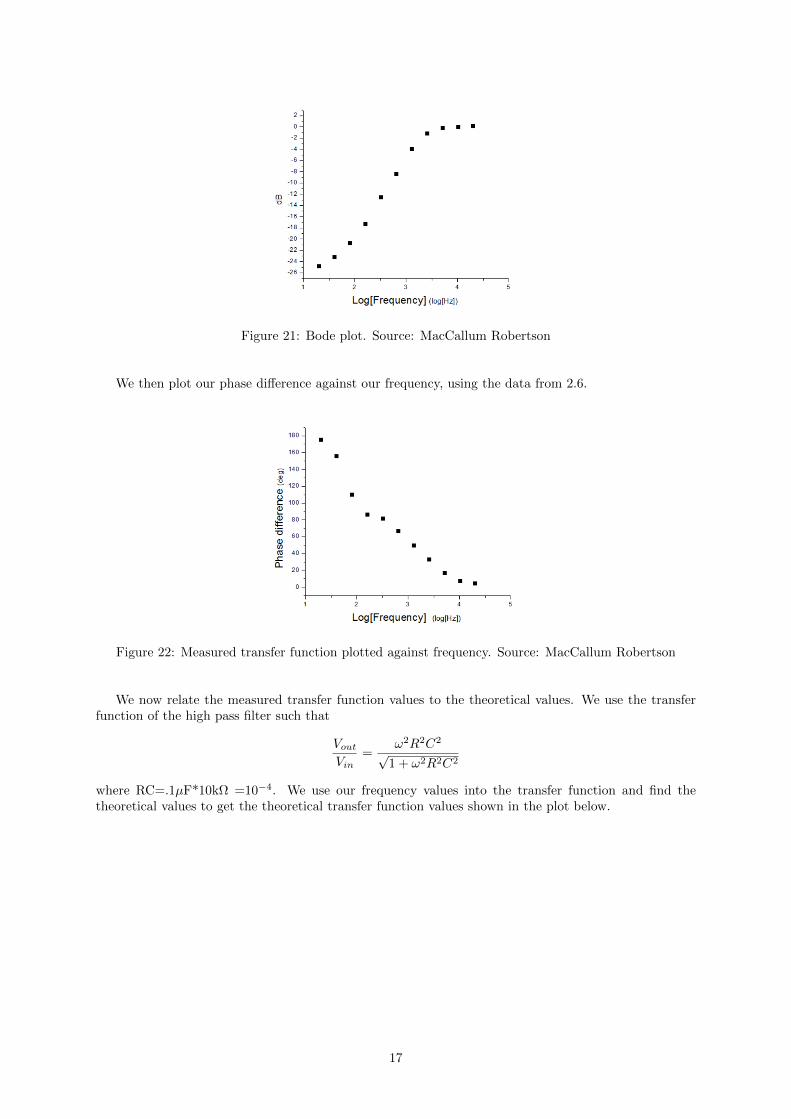
Figure 21: Bode plot. Source: MacCallum Robertson
We then plot our phase difference against our frequency, using the data from 2.6.
Figure 22: Measured transfer function plotted against frequency. Source: MacCallum Robertson
We now relate the measured transfer function values to the theoretical values. We use the transferfunction of the high pass filter such that
VoutVin
=ω2R2C2
√1 + ω2R2C2
where RC=.1µF*10kΩ =10−4. We use our frequency values into the transfer function and find thetheoretical values to get the theoretical transfer function values shown in the plot below.
17
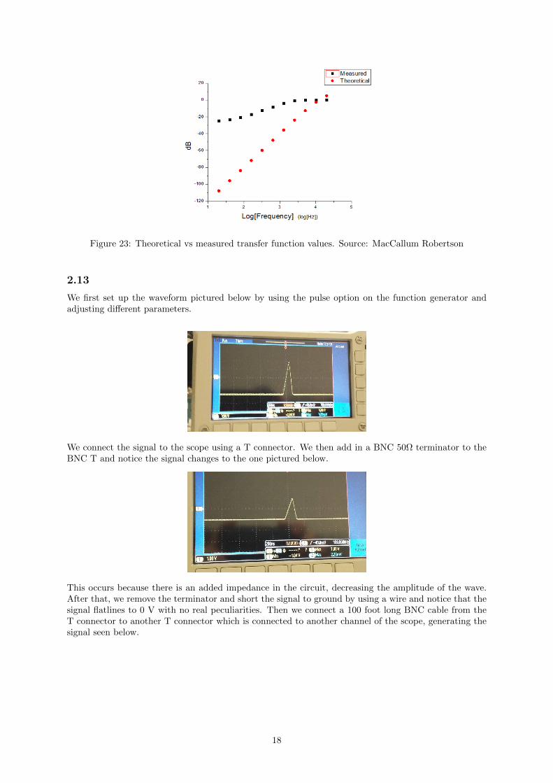
Figure 23: Theoretical vs measured transfer function values. Source: MacCallum Robertson
2.13
We first set up the waveform pictured below by using the pulse option on the function generator andadjusting different parameters.
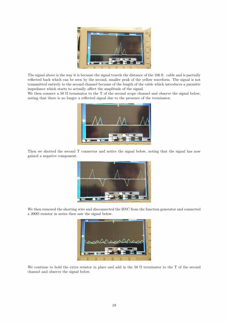
We connect the signal to the scope using a T connector. We then add in a BNC 50Ω terminator to theBNC T and notice the signal changes to the one pictured below.
This occurs because there is an added impedance in the circuit, decreasing the amplitude of the wave.After that, we remove the terminator and short the signal to ground by using a wire and notice that thesignal flatlines to 0 V with no real peculiarities. Then we connect a 100 foot long BNC cable from theT connector to another T connector which is connected to another channel of the scope, generating thesignal seen below.
18
The signal above is the way it is because the signal travels the distance of the 100 ft. cable and is partiallyreflected back which can be seen by the second, smaller peak of the yellow waveform. The signal is nottransmitted entirely to the second channel because of the length of the cable which introduces a parasiticimpedance which starts to actually affect the amplitude of the signal.We then connect a 50 Ω terminator to the T of the second scope channel and observe the signal below,noting that there is no longer a reflected signal due to the presence of the terminator.
Then we shorted the second T connector and notice the signal below, noting that the signal has nowgained a negative component.
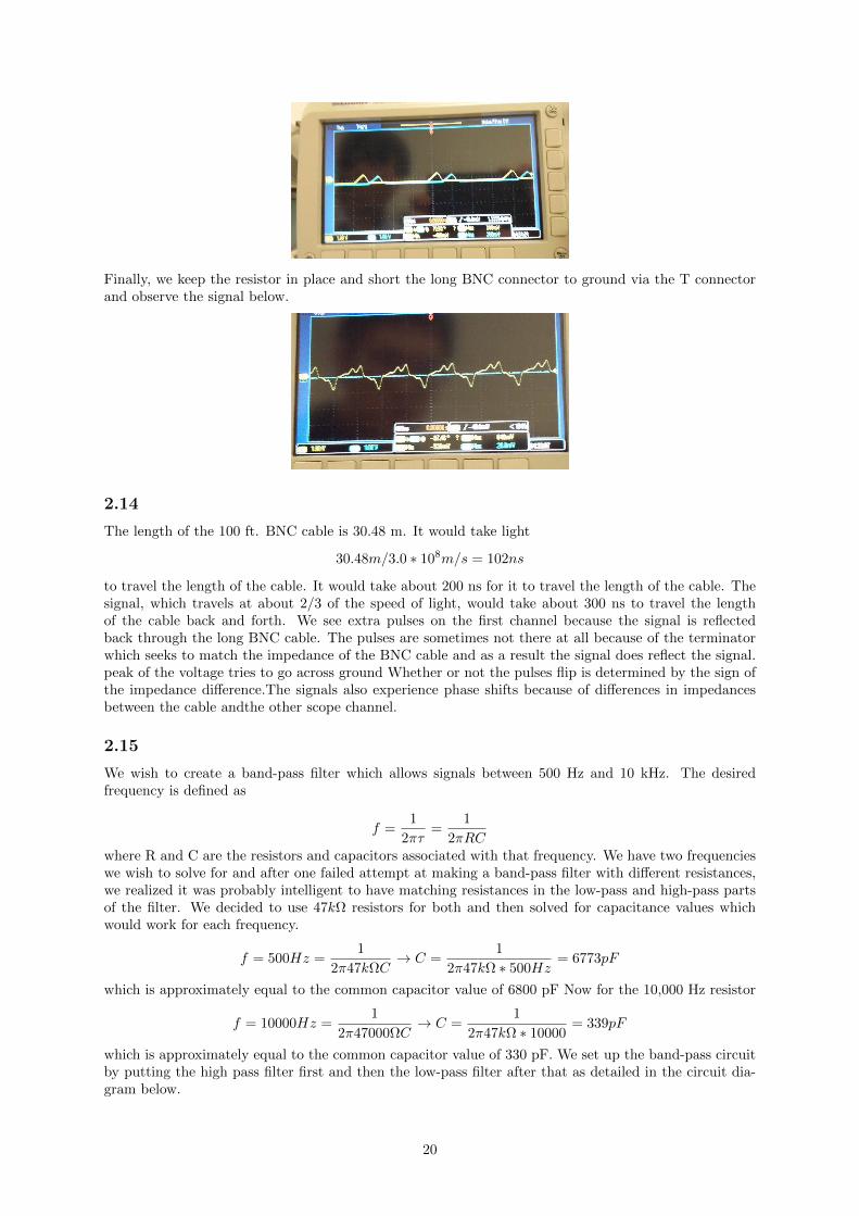
We then removed the shorting wire and disconnected the BNC from the function generator and connecteda 200Ω resistor in series then saw the signal below.
We continue to hold the extra resistor in place and add in the 50 Ω terminator to the T of the secondchannel and observe the signal below.
19
Finally, we keep the resistor in place and short the long BNC connector to ground via the T connectorand observe the signal below.
2.14
The length of the 100 ft. BNC cable is 30.48 m. It would take light
30.48m/3.0 ∗ 108m/s = 102ns
to travel the length of the cable. It would take about 200 ns for it to travel the length of the cable. Thesignal, which travels at about 2/3 of the speed of light, would take about 300 ns to travel the lengthof the cable back and forth. We see extra pulses on the first channel because the signal is reflectedback through the long BNC cable. The pulses are sometimes not there at all because of the terminatorwhich seeks to match the impedance of the BNC cable and as a result the signal does reflect the signal.peak of the voltage tries to go across ground Whether or not the pulses flip is determined by the sign ofthe impedance difference.The signals also experience phase shifts because of differences in impedancesbetween the cable andthe other scope channel.
2.15
We wish to create a band-pass filter which allows signals between 500 Hz and 10 kHz. The desiredfrequency is defined as
f =1
2πτ=
1
2πRCwhere R and C are the resistors and capacitors associated with that frequency. We have two frequencieswe wish to solve for and after one failed attempt at making a band-pass filter with different resistances,we realized it was probably intelligent to have matching resistances in the low-pass and high-pass partsof the filter. We decided to use 47kΩ resistors for both and then solved for capacitance values whichwould work for each frequency.
f = 500Hz =1
2π47kΩC→ C =
1
2π47kΩ ∗ 500Hz= 6773pF
which is approximately equal to the common capacitor value of 6800 pF Now for the 10,000 Hz resistor
f = 10000Hz =1
2π47000ΩC→ C =
1
2π47kΩ ∗ 10000= 339pF
which is approximately equal to the common capacitor value of 330 pF. We set up the band-pass circuitby putting the high pass filter first and then the low-pass filter after that as detailed in the circuit dia-gram below.
20
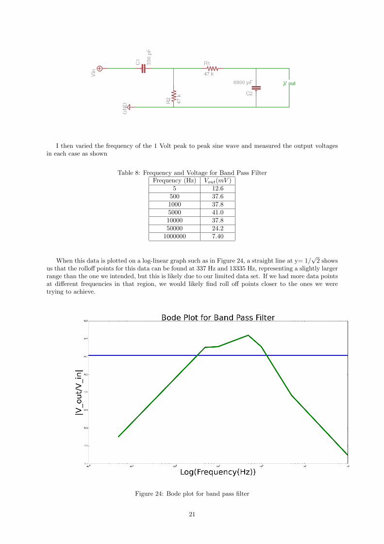
I then varied the frequency of the 1 Volt peak to peak sine wave and measured the output voltagesin each case as shown
Table 8: Frequency and Voltage for Band Pass FilterFrequency (Hz) Vout(mV )
5 12.6500 37.61000 37.85000 41.010000 37.850000 24.2
1000000 7.40
When this data is plotted on a log-linear graph such as in Figure 24, a straight line at y= 1/√
2 showsus that the rolloff points for this data can be found at 337 Hz and 13335 Hz, representing a slightly largerrange than the one we intended, but this is likely due to our limited data set. If we had more data pointsat different frequencies in that region, we would likely find roll off points closer to the ones we weretrying to achieve.
Figure 24: Bode plot for band pass filter
21

which shows that if we assume the voltage at 5 kHz to be essentially the max, the values in theband-pass filter’s range are let through without too much attenuation whereas the voltages drop a fairamount below and above the range of frequencies.
3 Conclusion
In this lab, we received an introduction to basic linear circuit components, primarily resistors and capac-itors as well as their associated impedances. We also learned a great deal about how to use importantelectrical equipment such as digital multimeters, oscilloscopes, and function generators. We also learnedhow to connect the DMM in series for current readings and in parallel for voltage readings. We learnedabout how input and output impedances can affect a signal’s reading and how to determine these twoby quantifying the relationship between the input voltage and current for some specific resistances. Welearned about the importance of Voltage dividers and Thevenin equivalent resistances and voltages andhow useful the the applications of the black-box are. We learned how to create basic high pass, low pass,and band pass filters
22