kmote - design and implementation of a low cost, low … · cost, low power hardware platform for...
TRANSCRIPT

KMote - Design and Implementation of a LowCost, Low Power Hardware Platform for
Wireless Sensor Networks
byNaveen Madabhushi
DEPARTMENT OF COMPUTER SCIENCE & ENGINEERING
INDIAN INSTITUTE OF TECHNOLOGY, KANPUR
May 2007

KMote - Design and Implementation of a LowCost, Low Power Hardware Platform for
Wireless Sensor Networks
A Thesis Submittedin Partial Fulfillment of the Requirements
for the Degree ofMaster of Technology
by
Naveen Madabhushi
to the
DEPARTMENT OF COMPUTER SCIENCE & ENGINEERING
INDIAN INSTITUTE OF TECHNOLOGY,KANPUR
May 2007

CERTIFICATE
It is certified that the work contained in the thesis entitled “KMote-Design andImplementation of a low cost, low power hardware platform for wireless sensornetworks” by Naveen Madabhushi has been carried out under our supervision andthat this work has not been submitted elsewhere for a degree.
May, 2007 Dr.Bhaskaran RamanDepartment of Computer Science & Engineering,Indian Institute of Technology,Kanpur-208016.
May, 2007 Dr.Kameswari ChebroluDepartment of Electrical & Engineering,Indian Institute of Technology,Kanpur-208016.
May, 2007 Dr.Rajat MoonaDepartment of Computer Science & Engineering,Indian Institute of Technology,Kanpur-208016.

Abstract
Wireless Sensor Networks (WSNs), as the name suggests consist of a networkof wireless nodes that have the capability to sense a parameter of interest like tem-perature, humidity, vibration etc. The sensed parameter is often relayed to a basestation through the network formed amongst these nodes. The devices used aretypically characterized by low cost, low power and are rugged in operation. Theyare commonly referred to as motes in the WSN domain. The usage of motes wasoriginally intended/ designed for military applications but soon spread to othercivilian applications like habitat Monitoring, environment monitoring, monitoringstructural health of railway bridges etc. Advances in hardware and wireless tech-nologies have facilitated rapid development of these tiny motes worldwide but theiravailability in India is not common.
Our work has been motivated by the need to develop such motes in India. Thisreport describes the design and implementation of a mote, which we call as KMote.The mote integrates programming, computation, communication, and sensing ontoa single system and provides an easy user interface for operating and deploying it.This report discusses the design challenges and hurdles involved in translating apaper design to a working prototype. Simplicity in design, low cost, and low powerconsumption were the primary considerations that influenced the design of KMote.This being our first effort in hardware design, we opted for a simplistic design andchose programming complexity in favour of hardware simplicity. We have imple-mented a prototype that is based on the telos design and integrates an MSP430microcontroller, CC2420 radio, 8 MB flash and an on board temperature sensor.We have tested and proved the operation of the microcontroller and the radio fortransfer of data over a wireless channel in 2.4 Ghz spectrum (ISM band). We havealso carried out outdoor experimental tests to determine the RF communicationrange of the KMote. We have obtained a range nearly double that of the TMote,the most popular commercial mote available in the market. At this range we wereoperating at an average RSSI of -84 dBm and experienced a packet error rate lessthan 1%. The bill of material cost of KMote is Rs 1625 and is less than onefourth of the selling cost of the Tmote (Rs 7740). Also, the administrative over-heads involved and large lead time for procurement of Tmote deters widespread useof motes in India. Therefore, the low cost of development of KMote makes it aviable option for fabricating such boards in India.
We believe that the experience and knowledge gained by developing this mote wouldbe beneficial to improve the existing prototype and aid in the easy availability ofsuch motes to research and educational communities in India, thus contributingto the growth of applications in the WSN domain. We also argue in favour ofdeveloping such motes in India due to the significant cost benefits offered by sucha development.

Acknowledgments
This thesis work has been a culmination of sustained endeavor and cooperationfrom various people directly or indirectly involved for the past one year. I wouldtake this opportunity to highlight the contribution from prominent people duringthe course of my thesis work. The mid course corrections provided by them havefacilitated the successful timely completion of the thesis.
At the very outset, I would like to express my sincere gratitude to Dr BhaskaranRaman who provided me the opportunity to work on this topic. His round theclock availability and guidance at various junctures was of immense help towardssuccessful completion of thesis. I am also grateful to Dr Kameswari Chebrolu andDr Rajat Moona who have been consistently involved in the supervision of theproject. Dr Rajat Moona has been of immense help in the hardware design, faultfinding and fixing. His involvement till the terminal stage of hardware fabricationand PCB testing coupled with his rich experience and knowledge was considerablyinstrumental in the speedy execution of the thesis. In addition, he has always beeninspirational ever since the inception of the project. I would also like to thank DrHarish who has spent a considerable amount of his time in teaching me the nu-ances of PCB and RF circuitry design.
I am grateful to Nilesh Mishra who was ever ready to help me out with pro-curement of hardware, soldering of components on the board. This work wouldbe incomplete without his involvement. I also thank Dr Parthasarathy Sensarmawho provided me unrestricted access to 4i Lab facilities. I would also like thankKumar and Renu, M Tech students of Electrical Department who took their timeoff from their work and taught me soldering of PCB boards.
In addition ,Lt Cdr DY Gokhale, Lt Cdr VP Singh, Lt Cdr DK Singh have pro-vided regular support in various activities related to experimental measurementsand brainstorming issues of technical relevance to the thesis.
Last but not the least, I would extend my sincere thanks to my wife Preethiand my family without whose support and co-operation, this work would havebeen incomplete.
Contents
1 Introduction 11.1 Introduction to Mote . . . . . . . . . . . . . . . . . . . . . . . . . . 11.2 Motivation and Problem Statement . . . . . . . . . . . . . . . . . . 21.3 Thesis Organization . . . . . . . . . . . . . . . . . . . . . . . . . . . 3
2 Background and Related Work 4
3 Design Considerations and Implementation 73.1 Hardware Design . . . . . . . . . . . . . . . . . . . . . . . . . . . . 73.2 Architecture of KMote . . . . . . . . . . . . . . . . . . . . . . . . . 103.3 PCB Design Issues . . . . . . . . . . . . . . . . . . . . . . . . . . . 113.4 Design of PCB in Protel DXP 2004 . . . . . . . . . . . . . . . . . . 133.5 Fabrication and Assembly of PCB . . . . . . . . . . . . . . . . . . . 153.6 Integration of KMote with TinyOS . . . . . . . . . . . . . . . . . . 16
4 Testing KMote and Results 184.1 Preparing the JTAG interface . . . . . . . . . . . . . . . . . . . . . 184.2 Testing the Microcontroller . . . . . . . . . . . . . . . . . . . . . . . 194.3 Testing the RF Circuit . . . . . . . . . . . . . . . . . . . . . . . . . 204.4 Radio Range Measurements . . . . . . . . . . . . . . . . . . . . . . 214.5 Power Consumption Measurements . . . . . . . . . . . . . . . . . . 224.6 Cost Analysis of KMote . . . . . . . . . . . . . . . . . . . . . . . . 224.7 Lessons Learnt . . . . . . . . . . . . . . . . . . . . . . . . . . . . . 24
5 Conclusions and Future Scope 26
Appendices 29A Schematics of Top Layer . . . . . . . . . . . . . . . . . . . . . . . . 29B Schematic of Bottom Layer . . . . . . . . . . . . . . . . . . . . . . 30C Procedure to Connect External Antenna to KMote . . . . . . . . . 31D Steps Involved in Integrating KMote with TinyOS . . . . . . . . . . 32E Procedure to load programs on to KMote using JTAG and gdb . . . 33
iv
List of Tables
2.1 Evolution of Mote.(Source - Telos:Enabling ultra-low power wirelessresearch,IPSN ’05) . . . . . . . . . . . . . . . . . . . . . . . . . . . 5
2.2 Comparison of Popular Motes . . . . . . . . . . . . . . . . . . . . . 6
3.1 Comparison of CC2420 and XE 1205 Radio chips . . . . . . . . . . 83.2 Range measurements on Narrow road / airstrip (Line-of-sight envi-
ronment) . . . . . . . . . . . . . . . . . . . . . . . . . . . . . . . . . 9
4.1 Power Consumption of KMote . . . . . . . . . . . . . . . . . . . . . 224.2 Bill of Material Cost of KMote . . . . . . . . . . . . . . . . . . . . 234.3 Cost Comparison of Motes . . . . . . . . . . . . . . . . . . . . . . . 23
v
List of Figures
3.1 Architecture of KMote . . . . . . . . . . . . . . . . . . . . . . . . . 103.2 Serial Interface for KMote . . . . . . . . . . . . . . . . . . . . . . . 12
4.1 JTAG Interface for KMote . . . . . . . . . . . . . . . . . . . . . . . 194.2 Experimental Setup . . . . . . . . . . . . . . . . . . . . . . . . . . . 21
1 Schematic of (Top Layer) . . . . . . . . . . . . . . . . . . . . . . . . 292 Schematic of KMote (Bottom Layer) . . . . . . . . . . . . . . . . . 303 Position of capacitors C13 and C14 . . . . . . . . . . . . . . . . . . 31
vi

Chapter 1
Introduction
The advances in the hardware and wireless technologies have resulted in inexpen-sive low power communication devices that can be deployed throughout a physicalspace, providing dense sensing close to physical phenomena, processing and com-municating this information, and coordinating actions with other nodes. Such adeployment can be termed as a Wireless Sensor Network (WSN). To realize sucha network, we must address a new collection of challenges. The individual devicesin a WSN are inherently resource constrained: they have limited processing speed,storage capacity, battery capacity, and communication bandwidth. These deviceshave substantial processing capability in the aggregate, but not individually. Theseindividual devices are referred to as motes in WSN domain.
1.1 Introduction to Mote
The term mote refers to a tiny particle and these embedded devices for usein a WSN are essentially tiny in size and hence the name. These nodes haveprocessing and computational capability and generally consist of an RF trans-receiver, memory, on board sensors/actuators and a power source. Some of therequirements of a mote for their use in applications are as under:
• The ability to have some amount of on board processing.
• They should be able to communicate over the air and also have some basicnetworking capability.
• The motes should be alive for extended periods (up to a few months to ayear) of deployment. Therefore they should be able to operate at low power.
• They should have sensors/actuators embedded in them so as to interact withthe environment in which they are deployed and communicate the sensedparameter to a central location.
To be able to fulfill the basic requirements as mentioned above, a mote shouldhave the following components:
• Microcontroller
1

• Radio
• An embedded sensor or the ability to connect to sensors/sensor boards.
• On board memory: RAM, Flash.
• Power source
The usage of motes was originally intended for military applications but soonspread to other civilian applications like habitat monitoring [18, 22], environmentmonitoring [23, 21], volcano monitoring [25], wildlife tracking [15], industrialmonitoring [17], structural monitoring [16]. These experimental deployments haveenabled researchers and scientists across the globe to study effects/interactions innature which was earlier not possible with wired technologies due to hurdles likehostile environment, physical hurdles in reaching a place etc.
1.2 Motivation and Problem Statement
There are a number of commercial off-the shelf (COTS) motes available in themarket today but none of them are readily and easily available in India. Therehas been a similar development at IIT Delhi [3], wherein they developed Rete, amote which operates at 433 Mhz. However, these motes have their sales division inUSA and are not readily available in India. Moreover, the COTS motes have to beimported and not all educational institutions in the country have administrativeprocedures in place that enable them to procure these devices easily. It is thereforeimportant that such devices are easily and readily available to the educational andresearch communities in India. Each of these motes costs a few thousands ofrupees and thus are still costly enough to deter widespread use in educationaland research institutes. Hence, the cost of these devices should be low enoughto encourage their widespread use. With an increase in awareness about thesedevices, it is realistic to assume that new applications are developed which caterto the problems specific to India.
We therefore define our problem statement as: to design and implement a lowcost, low power hardware platform for use in wireless sensor networks. Therefore,the main goals that we seek to address in this work are the following:
• Design of a low cost, low power hardware platform for use in sensor networks.
• Build a simple working prototype that can be improved upon. The prototypethough simple should be able to deliver all the functionalities possible withcommercially available state of the art motes.
• The motes developed should be easily available for research and educationalinstitutions.
We have designed and implemented KMote which integrates an MSP430 micro-controller, a CC2420 radio chip which operates in the Industrial, Scientific andMedical (ISM) band (2.4 Ghz). An 8 Mb flash for data logging and a temperaturesensor have also been embedded into the platform. We have integrated KMotewith an open source embedded operating system TinyOS so that it can be readilyprogrammed for custom applications. The development cost of KMote is Rs 1625

and is less than one fourth the cost of the most popular commercially availablemote, Tmote, which costs Rs 7740. We have tested the building blocks of themote: microcontroller and radio circuitry for their correct operation. We havealso carried out range measurements and have observed ranges nearly twice thatof Tmote. The mote is powered by two AA batteries or 3.0 volts power source andconsumes about 20 mA during transmission.
1.3 Thesis Organization
The rest of the report is organized as follows. Chapter 2 discusses the evolutionof various motes and comparison of commercially available motes. Chapter 3discusses the design considerations and implementation of KMote. In this chapterwe discuss the hardware choices available and the reasons for choosing the hardwareused in KMote. We also discuss the architecture of KMote and design issues whiletranslating the paper design to a working model in the section on PCB design. Wealso discuss our design experiences during the fabrication and integration of themote with TinyOS in this chapter. Chapter 4 discusses the testing methodology ofKMote and the results obtained during the range and power consumption tests. Wefinally summarize our work in Chapter 5 and discuss the future scope in Chapter6. The appendices at the end of the report give detailed schematics of the mote,bill of material required, procedure for integration of mote with TinyOS and theprocedure to connect an external antenna to the mote to achieve higher ranges.

Chapter 2
Background and Related Work
The usage of motes was conceived and implemented by the Smart Dust [24]project. The Smart Dust project explored the possibility of using motes to forma massive distributed network. The main goal of the project was to explore microfabrication technology’s limitations and study the feasibility of such a platform.Because of the mote’s discrete size, substantial functionality, connectivity, andanticipated low cost, Smart Dust was envisaged to facilitate innovative methodsof interacting with the environment, and provide more information from physicalregions less intrusively. The intended applications for smart dust were:
• Deploy sensor networks rapidly by unmanned aerial vehicles or artillery inbattlefield scenarios and track enemy movements.
• Tracking the movements of birds, small animals, and insects and understandtheir behavioral patterns
• Monitor health of rotating machinery and understand the reasons for high-cycle fatigue.
There have been a number of platforms which were developed on the lines ofsmart dust motes. The initial devices incorporated small microcontrollers (8 bit,4 KB flash) and a simple radio (4 Kbps data rate) and their life time was up to amaximum of 2 years. Table 2.1 taken from [19] shows the evolution of mote from1998. The figure also depicts the relative capabilities of the mote as it evolved.
As can be seen from the table, the main focus in the design of the motes islow power of operation. Almost all the microcontrollers used in various designsoperate at low voltages of 2.7 volts to 3.6 volts. Another important factor forthe choice of microcontroller is the current drawn during its sleep and wake uptime. Low sleep current and low wake up times minimise the duty cycle of a moteand therefore extends the life of a mote and consequent network life time. Telosdesign uses MSP430 microcontroller which has lowest sleep and wake times ascompared to the other microcontrollers operating at low voltages. On-chip RAMalso plays a vital role in the processing capability of the mote and MSP430 offersthe maximum on-chip RAM in comparison. Another salient factor in the mote’sevolution is their usage of radio chips for communication. With the introduction of
4

Mote Type WeC Rene Rene2 Dot Mica Mica2DotMica2 Telos(Year) 1998 1999 2000 2000 2001 2002 2002 2004
Processor AT90LS8535 ATMega163 ATMega128 MSP430Radio Chip TR1000 CC1000 CC2420Flash 32 KB 512 KB 128 KBSensors No on-board sensors Yes No on-board sensors YesFrequency of Operation 916.5 Mhz 868 Mhz 2.4 GhzTransmit Power 0 dBmMax Data Rate 10 Kbps 40 Kbps 38.4 Kbps 250 KbpsPower Consumption 36 mW 42 mW 35 mWSleep Power (µW) 45 75 6wakeup Time (µS) 1000 36 180 6Interface IEEE 1284 and RS232 USB
Table 2.1. Evolution of Mote.(Source - Telos:Enabling ultra-low power wireless research,IPSN ’05)
802.15.4 standard for wireless sensor networks, the motes too started incorporatingchips that use these standards for interoperability of platforms.
A comparison of state-of-the art popular motes is shown in Table 2.2. As seenfrom the table, Tmote offers the best functionalities compared to the other motes.However, the cost of these motes is quite expensive and are not readily available foreducational/research institutions in India. These motes need to be imported andnot all educational institutes have administrative procedures in place for importingthem. Moreover, the lead time involved in procurement is in the order of a fewmonths and such a large time deters their widespread use. There has been a similardevelopment at Technology business incubation unit of IIT Delhi called Rete [3].Rete is a mote that is developed as part of CpiderNet, a complete sensor networkinfrastructure consisting of motes, self configuring networking stack and softwarefront-end for data-analysis and network management. Although, Rete has beendeveloped at IIT Delhi, these motes are marketed and sold by a US based companyElfSys. It is therefore evident that motes that cater to Indian requirements are noteasily and readily available for educational/research institutions. Rete operates at433 Mhz which is not unlicensed in India. The usage of this frequency is restrictedto demonstration of equipment/ for amateur radioists but is not permitted forcommercial use.
The design and development of KMote is based on Telos design. The cost ofresearch prototype of KMote is Rs 1625 which is significantly lower than the costof Tmote which is priced at Rs 7740. Moreover, procurement of these motes incurand additional shipping charges which are the order of the cost of a couple ofKMotes. We therefore, believe that easy availability of KMote coupled with lowcost would facilitate growth of WSN applications that cater to specific problemsof India.

MicaZ Tmote Tiny NodeProcessor AT Mega 128 MSP430 MSP430Radio Chip CC2420 CC2420 XE 1205Flash 512KB 8MB 4MBSensors No on board sensors Humidity Light
Light TemperatureFrequency of Operation 2.4 Ghz 2.4 Ghz 868-870 MHzTransmit Power 0 dBm 0 dBm 0 to +12 dBmMax Data Rate 250 Kbps 250 Kbps 152.3 KbpsMax Range upto 70m upto 150m 200m @ 76.8 Kbps(outdoors)Power Consumption 28 mA 21mA @ 0dBm 25mA @0dBm(Max) 62mA @ +12 dBmInterface USB/Serial USB SerialOperating System TinyOS TinyOS TinyOSCost 125 130 (without sensors) 180(USD) 180(with sensors)
Table 2.2. Comparison of Popular Motes

Chapter 3
Design Considerations and
Implementation
A good design forms the building block for any successful hardware implemen-tation. It is also the most important aspect and involves multiple revisions andevaluations to identify and correct any errors. When we started off with the designof KMote, we decided on the following as general guidelines of our design:
• The design should have all the characteristics of a mote: low cost, low powerconsuming, flexible platform.
• Keep the first design as simple as possible and opt for programming complex-ity in favour of simplistic hardware. This being our first effort in hardwaredesign, a simpler design is a good starting point to avoid any challengesarising from inefficient hardware design.
• The design should be such that it should have the functionality of the stateof the art motes available commercially.
In this chapter we present the design choices involved and considerations thereof.We explain the choice of hardware for our platform and the architecture chosento implement this platform. We also discuss the design challenges involved inPCB design and explain the choices made. We finally explain the process involvedin translating the software design to fabrication of PCB and its integration withTinyOS, the embedded Operating System.
3.1 Hardware Design
In this section we discuss the hardware chosen for KMote and mention themodifications and enhancements carried out on an existing embedded platformdesign. With the design guidelines in place, the next step was identification ofhardware to suit our requirements. We chose to stick to the hardware used intelosb [7] as the advantages offered are dual:
7
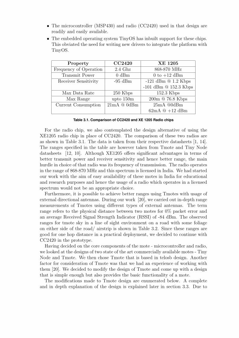
• The microcontroller (MSP430) and radio (CC2420) used in that design arereadily and easily available.
• The embedded operating system TinyOS has inbuilt support for these chips.This obviated the need for writing new drivers to integrate the platform withTinyOS.
Property CC2420 XE 1205Frequency of Operation 2.4 Ghz 868-870 MHz
Transmit Power 0 dBm 0 to +12 dBmReceiver Sensitivity -95 dBm -121 dBm @ 1.2 Kbps
-101 dBm @ 152.3 KbpsMax Data Rate 250 Kbps 152.3 Kbps
Max Range upto 150m 200m @ 76.8 KbpsCurrent Consumption 21mA @ 0dBm 25mA @0dBm
62mA @ +12 dBm
Table 3.1. Comparison of CC2420 and XE 1205 Radio chips
For the radio chip, we also contemplated the design alternative of using theXE1205 radio chip in place of CC2420. The comparison of these two radios areas shown in Table 3.1. The data is taken from their respective datasheets [1, 14].The ranges specified in the table are however taken from Tmote and Tiny Nodedatasheets [12, 10]. Although XE1205 offers significant advantages in terms ofbetter transmit power and receiver sensitivity and hence better range, the mainhurdle in choice of that radio was its frequency of transmission. The radio operatesin the range of 868-870 MHz and this spectrum is licensed in India. We had startedour work with the aim of easy availability of these motes in India for educationaland research purposes and hence the usage of a radio which operates in a licensedspectrum would not be an appropriate choice.
Furthermore, it is possible to achieve better ranges using Tmotes with usage ofexternal directional antennas. During our work [20], we carried out in-depth rangemeasurements of Tmotes using different types of external antennas. The termrange refers to the physical distance between two motes for 0% packet error andan average Received Signal Strength Indicator (RSSI) of -84 dBm. The observedranges for tmote sky in a line of sight environment on a road with some foliageon either side of the road/ airstrip is shown in Table 3.2. Since these ranges aregood for one hop distance in a practical deployment, we decided to continue withCC2420 in the prototype.
Having decided on the core components of the mote - microcontroller and radio,we looked at the designs of two state of the art commercially available motes - TinyNode and Tmote. We then chose Tmote that is based in telosb design. Anotherfactor for consideration of Tmote was that we had an experience of working withthem [20]. We decided to modify the design of Tmote and come up with a designthat is simple enough but also provides the basic functionality of a mote.
The modifications made to Tmote design are enumerated below. A completeand in depth explanation of the design is explained later in section 3.3. Due to

Average Pkt Error (%) Average RSSI (dBm)Tx-Rx Dist.(m)
(Std. Dev.) (Std. Dev.)
Internal Antenna at ReceiverInternal-60m 0.18 (1.03) -81.11 (2.97)
Internal-75m 1.37 (4.34) -83.74 (3.61)
Omni-60m 0 (0) -81.92 (0.49)Omni-75m 0 (0) -80.64 (2.47)Omni-90m 35.92 (33.42) -94.91 (1.6)
Sector-210m 0 (0) -81.92 (0.49)Sector-310m 1.02 (4.3) -91.85 (0.81)Sector-400m 0.62 (2.24) -92.33 (1.03)Sector-500m 0 (0) -90.12 (0.5)
Grid-90m 0 (0) -75.35 (1.36)Grid-210m 0.03 (0.18) -75.825 (2.37)Grid-300m 0 (0) -80.42 (1)Grid-400m 0 (0) -82.21 (0.9)Grid-500m 0 (0) -85.67 (0.94)
Omni Antenna at the ReceiverOmni-90m 0.04 (0.33) -80.92 (0.88)Omni-150m 7.63 (12.46) -90.86 (0.64)
Sector-500m 0.13 (0.68) -80.92 (0.88)Sector-600m 0.07 (0.25) -89.48 (0.35)Sector-700m 0.5 (1.05) -91.22 (0.34)Sector-800m 3.42 (4.83) -91.58 (0.41)
Sector-30m 13.01 (14.37) -90.01 (3.91)
Grid-500m 0.12 (0.49) -75.25 (0.07)Grid-600m 0.07 (0.25) -79.85 (0.24)Grid-700m 0.15 (0.61) -82.07 (0.2)Grid-800m 0.13 (0.39) -85.76 (0.31)
Table 3.2. Range measurements on Narrow road / airstrip (Line-of-sight environment)

the modifications mentioned below, the form factor of the KMote increased ascompared to that of Tmote.
(a) Provision of serial interface in lieu of USB.
(b) Provision of external power supply adapter.
(c) on-board temperature sensor.
(d) LCD panel interface.
(e) Increase in unused GPIO pins.
3.2 Architecture of KMote
Figure 3.1. Architecture of KMote
The architecture of KMote after incorporation of features as mentioned aboveis shown in Figure 3.1. The microprocessor being the building block becomes thecore of the platform and the functionality of the mote is built around it. Radio,the other building block of the mote, is interfaced to it using the SPI bus. Wechose SPI as full-duplex capability of this bus makes it simple and efficient foran application that has single master and one/two slaves. The other choice wasusage of I2C bus. SPI bus supports data rates upto 20 Mbps while the commondata rates of I2C bus are 100/400 Kbps. This aspect made us choose SPI as thecommunication bus. In addition to the SPI bus, the radio needs an interface forDigital I/O, Clear Channel Assessment (CCA), Start Frame Delimiter (SFD) pins.I/O pins of microcontroller are used for this purpose.

In order to radiate electromagnetic energy, the mote needs an antenna. We chosean Inverted F Antenna (IFA) for this. This antenna is recommended by Chipcon[4] for usage with CC2420. This antenna has an omni directional radiation patternand is therefore useful in typical applications where motes are used. To achievehigher ranges, a provision for connecting external antenna is required. This isachieved by providing a Sub-Miniature Version A (SMA) connector which can beconnected to a 50 Ω antenna. The procedure for connecting an external antennato the mote is described in Appendix C.
To enable data logging and storage, the microcontroller is interfaced to a flashSTM25P80. This chip has a memory of 8 Mb, operates at low voltages of 2.7 to3.6 volts and has an SPI interface [8]. We chose this for low operating voltagesand good storage capacity. The flash is interfaced through SPI bus and thesecommunication lines are shared with the radio. Hence, careful bus arbitration isrequired while using any one of them.
In many teaching and research applications, it is useful to have an embeddedsensor on a mote. Therefore we interfaced a temperature sensor with the ADCpins of the microcontroller. We have also provided a JTAG interface to enabletesting and debugging of the platform.
Another important requirement of a mote is its ability to interface peripherals.Universal Asynchronous Receiver/Transmitter (USART), Inter-Integrated Circuit(I2C) bus and General Purpose Input Output (GPIO) pins of the microcontrollerare used for this purpose. These pins are brought out in the form of expansionconnectors and peripherals can be connected to them.
In general, for teaching and research purposes, it is useful to have an on-boardLCD that aids in better understanding of the functioning of the mote, Also, dur-ing our work [20], we felt the need for a better debugging interface than the LEDsprovided on Tmote. We wanted to be able to printout some debugging messageswhich are more useful than just using three LEDs for diagnostic purposes. Wetherefore included an interface with LCD panel in our design. In addition to de-bugging, the presence of an LCD panel can also be used for instructional purposes.This panel is interfaced with GPIO pins of the microcontroller.
3.3 PCB Design Issues
After deciding the necessary modifications in telosb design, we incorporatedthem in our design. Incorporating the modifications and keeping the design assimplistic as possible was challenging and we had to give in for some programmingcomplexity in favour of hardware simplicity. The design challenges we encounteredand consequent decisions are enumerated in subsequent paragraphs.
(a) Provision of a serial interface in lieu of USB. This interface is pri-marily for programming the mote from a PC/Laptop and also for transferof data from a mote to PC. Provision of a serial interface is in accordancewith our goal of reducing circuit complexity of the PCB. Also, from the ex-periences of researchers in [25], we felt that, a serial interface is a lot more

advantageous when the motes are interfaced with external devices like GPSwhich have serial ports as their primary mode of communication.
Figure 3.2. Serial Interface for KMote
A simplified block diagram of connections between the serial port and MSP430in KMote is shown in Figure 3.2. The microcontroller has UART interfacethat supports RS 232 protocol. We have used MAX3380 [5] which has twotrans-receivers and converts voltages from TTL (used by MSP430) to RS232 (used by Serial Port). In addition to the connections shown in the figurebetween the chips and serial connector, MSP 430 needs a signal to reset thedevice before it is put into programming mode of operation. It is desirable toput the processor in programming mode in somewhat an automated mannerfrom the PC. This can be achieved with the use of modem control signalson RS232. However these signals use ±15 V signalling. MAX 3380 has onlytwo trans-receivers and both of the receivers are used to drive UART0X andTCK of MSP430 thereby leaving no spare pin to convert the signals to TTLlevel and to drive reset for MSP430. There were two choices available forus to reset MSP430: (i) To use another MAX 3380 chip and wire the resetpin of MSP430 to one of the receivers (ii) To use only one MAX 3380 chipand use a reset switch of the mote to reset the microcontroller. We chosethe latter as we wanted to use minimum components on the PCB therebysimplifying the design.
(b) Provision of external power supply adapter. Since the USB interfacehas been done away with, there was a requirement for external power sourceto power the mote. This power supply is the primary power supply for themote with batteries as the secondary mode of power source. Consequently,we designed a voltage regulation circuit to regulate the external power supply.We used the MCP1700-3302 [13] voltage regulator chip for this purpose. Thechip gives a regulated power supply of 3.3 volts for an input power supply ofupto 6 volts.
(c) on-board temperature sensor. The Tmote design has on-board humid-ity and pressure sensors. These sensors were interfaced with GPIO pins of
microcontroller. We felt that it would be convenient if we brought theseGPIO pins out as headers thereby providing greater flexibility in interfacingof different kinds of peripherals with the mote. Therefore, we removed thesesensors from our design and interfaced an on-board sensor to demonstratethe proof of concept of a sensing application and brought out the remainingGPIO pins to the external headers. Removal of these sensors also helped inbringing down the cost of the mote. We used the Analog Devices TMP36FSZsensor which has an operating range of -40 to +125oC [9]. The sensor oper-ates at Vcc = 2.7V and this supply was provided from microcontroller itselfusing a GPIO pin.
(d) LCD panel interface. A GPIO based 2x16 character LCD panel interfaceis provided to aid programmers in debugging the applications on the mote.This was a major drawback in Tmote wherein the programmer had accessonly to 3 on-board LEDs for debugging and this proved inadequate for quickdebugging. We were faced two alternatives for choice of LCD Panel: (i)LCD Panel without on-board controller and (ii) LCD panel with on-boardcontroller. MSP430 F1611 does not provide any LCD controller and so wechose an LCD panel with an integrated controller.
(e) Increase in unused GPIO pins. As discussed in (c) above, the numberof unused GPIO pins in KMote have been increased to 26. This would allowa larger number of GPIO based peripherals to be interfaced with KMote.With the addition of LCD panel and external power supply adapters, therehas been an increase in the form factor of the board as compared to thatof Tmote. With an increase in form factor, we were also able to provide anadditional mounting hole to improve mechanical the strength of the mote.
3.4 Design of PCB in Protel DXP 2004
This section discusses the our design experience during designing the PCB inProtel DXP. We feel these experiences will be useful for future developers and sodiscuss them in detail.
The schematics and PCB of KMote were designed in Protel DXP 2004. Drawingof the schematic was fairly easy but it took us quite some time to translate theschematic to a PCB design. Protel is a very good software but has a steep learningcurve. It took us about a month to explore all the features and capabilities ofthe software. Although the available documentation is exhaustive, it is poorlyorganised. We had to design footprints for most of the components in use as thefootprints made available by the respective manufacturers were not compatiblewith Protel. Since we had decided upon the choice of components in advance andordered them as well, it was easy to design footprints. In retrospect, this was awise decision as choosing a component and designing a footprint for it is the notthe correct way. This is because, there were instances where we chose a certaincomponent but the lead time for procurement was as large as 2-3 months that wehad to discard that and look for an alternative. This is a factor specific to India,
as we ordered our components from suppliers based in USA. This is because it waseasier to locate and order from these suppliers on internet. However, during thecourse of our work, we realised that many of components which were ordered fromUSA are also available through suppliers based in India. Integration of footprintsalso took a lot of time as this was the first experience for us in using ElectronicDesign Automation (EDA) software.
Just when we thought that it would be easy to design PCB once the footprintsare integrated, we realised that the job was not that simple. A major challenge wasthe decision on the track thickness for connecting the output of Radio to the on-board antenna. The width of the track determines the characteristic impedance,Z0 of the transmission line connecting the power output from radio to the feed ofthe antenna. The footprint of the antenna was taken from the Chipcon ApplicationNote [4]. Although there exists detailed formulae to compute the track width, wechose a width of 0.4 mm as per the design of Tmote. There was also a requirementof placing a large number of grounded vias around the path of radiation to minimiseRF radiation due to the leakage of radiated power to other parts of the board.
The choice of minimum track width and minimum diameter of plated throughholes was another tricky issue. Routing of wires between the components on theboard becomes a lot easier if these dimensions are small. However, manufacturercannot fabricate a PCB below certain minimum dimensions. So, we contacted themanufacturer and confirmed his limitations to be 6 mils and 12 mils as minimumtrack width and minimum diameter of via respectively. We chose a minimumdimension of 6 mils for track width and 20 mils for via diameter and designed theboard accordingly. We chose the clearance width to be 0.4 mm between tracksand vias to prevent any accidental short circuiting of the tracks while solderingthe components.
The choice of discrete components for radio circuit was as per the guidelinesmentioned in the datasheet [1] and most of them were components with footprint0402 . However, the solder side of the board where microcontroller was placed, didnot have any restriction on the size of the components and we chose componentswith footprint 0805. All the components chosen were Restriction of HazardousSubstances (RoHS) complaint and lead free. The schematics of the top and bottomlayers of KMote are present at Appendix A and Appendix B respectively.
The final PCB was a 4 layered one with dimensions of 2 inch by 3 inches.The entire process of generating a gerber file for manufacture of PCBs from theconceptualisation took us about 5 months. This large time frame was mainly dueto our lack of experience in PCB design and also due to the number of revisionswhich went into each stage of the design. It is pertinent to mention that, as anaside to this process, we experimented with designing a simple accelerometer boardfor use with Tmotes for the BriMon (reference) application. The experience gainedin designing and fabrication of these accelerometer boards was immensely helpfulin our design of KMote which highlighted the role of experience in such a process.

3.5 Fabrication and Assembly of PCB
The PCB material specifications are the following:
(a) 4 Layer PCB 1.0 mm FR4. The total thickness of the board is 1.0 mm andthe material is Flame Retardant woven glass reinforced epoxy resin.
(b) Layer Spacing:
– 1-2: 0.25 mm
– 2-3: 0.4 mm
– 3-4: 0.25 mm
(c) 1 oz copper pour, solder plated finish
There were a number of revisions of design due to the interaction with themanufacturer. Ultimately, the fabricated PCBs were received by us only in thethird week of March 07.
The next major and very important task in the development cycle of an em-bedded system is assembly of components on the fabricated PCB. This is not aneasy task as there were specialised chips like CC2420 that needed a lot of carewhile soldering. Also, the form factor of the components used were very small.We were novices vis a vis soldering and manual soldering of the components onthe board was strictly not an option if we wanted the board to work. There werehowever two options: (i) Assemble the board at IIT Kanpur itself by making use ofsoldering facilities in the 4i lab. (ii) Offload the soldering process to a professionalfirm identified in Bangalore. We identified the firm in Bangalore as the firms wecontacted in Kanpur/Delhi were not eager to take up orders in small quantitiesand required a minimum order of at least 100 or more. We had sufficient compo-nents to assemble five boards and so decided to solder one board in IIT Kanpurand offload the rest to the firm in Bangalore.
The process of soldering the board in 4i lab was very helpful in understandingthe circuit better and also in getting experience in soldering these tiny components.The soldering experience came in handy while debugging the hardware for errors(this will be explained in detail in Chapter 4). We carried out soldering of thesecomponents in three phases. In the first phase, we used the IR soldering machineto solder MSP430. This was a first time for us to use the machine and the processthough intimidating initially, was fairly simple and easy. The machine uses vacuumbased tip to pick up the component and with a magnification of 10x available forthe user, it was very easy to align the component on to the pads on the PCB. ThePCB was tinned during the fabrication process and so we did not tin the boardsfurther. Once the chip was aligned with the pads, it was placed on the pads andInfra Red radiation was used to heat the chip evenly and solder the pins to itspads.
The next phase involved correct placement and alignment of remaining compo-nents on their respective solder pads. We then used the LPKF reflow solderingmachine to evenly heat the board and solder the components. The process is verysimple and convenient and the only time consuming process in this type of sol-dering is the alignment and placement of components on their respective solder

pads. With this method, one can solder upto 10 boards of our PCB size at onego. We however, soldered only one board. After soldering the solder side of theboard, we used reflow process to solder the component side as well. We manuallysoldered expansion headers, switches and power supply jack later on completionof soldering the components.
However, the soldered board did not work as there were a number of dry solderpoints on the PCB. This is because we soldered the components directly to thetinned pads without tinning the PCB. We later learned that this is not a goodpractice and boards have to be tinned before soldering them.
The other four boards along with the components were soldered at PeninsulaElectronics, Bangalore. Five PCBs were all assembled and ready for testing by thesecond week of April. There was no other way to test the mote than to integrateit with TinyOS, load an application and check for correct functionality of theprogram. Once the boards were powered up and tested through JTAG for correctdetection of MSP430, we went ahead with the process of integration of KMote withTinyOS. A detailed explanation of testing the mote through JTAG is explained inChapter 4.
3.6 Integration of KMote with TinyOS
An embedded hardware platform is only useful if it can be programmed to runa desired application. To achieve this, the platform needs to be integrated withan embedded operating system. There are many embedded operating systemsavailable but we chose TinyOS as the operating system. TinyOS is an open sourceOS developed for embedded systems at U.C.Berkeley and supports both MSP430and CC2420. Another major factor for choice of TinyOS as the operating systemis the fact that we were experienced in its usage and quite comfortable with itsstructure and design.
After successful completion of fabrication and assembly of KMote, it was neces-sary to integrate it with TinyOS. We chose to integrate it with the current versionof TinyOS, i.e. TinyOS 2.x. The steps involved in integration are fairly simple andstraightforward. As mentioned earlier, TinyOS supports multiple platforms (e.g.MicaZ, Mica, Tmote, TinyNode etc) and the structure of TinyOS is such that itreuses as much code as possible between platforms. The platforms support eitheror all the chips supported by TinyOS and so writing platform specific code to usethe same chips all over again does not make sense. The chip on a particular plat-form maybe physically wired differently in each platform but the logic that drivesthe platform is platform independent. We made use of this platform independenceoffered by TinyOS to integrate KMote with it.
Therefore, all the chip specific directories contain platform independent code.Integrating a new platform is then a matter of pulling in the code for each of theplatform’s chips, and linking them together. The steps involved in integrating ofa KMote with TinyOS are explained in detail in Appendix D. These steps ensurethat the basic skeleton of KMote is successfully integrated with TinyOS. Thismeans that TinyOS recognises KMote and that platform definitions for TinyOS

are in place. However, this is not sufficient to program the device as there is noplatform specific code to drive the low level hardware which is specific to eachhardware. We cover the explanation of methodology for testing and enabling theplatform for programming in the chapter 4.

Chapter 4
Testing KMote and Results
Testing KMote was the last major phase in its development. As discussed inthe previous chapter, the KMote is integrated with TinyOS. In this chapter, wewill discuss the procedure to prepare the mote for programming. To be able toprogram the mote, MSP430 needs to be put into programming mode and hencebootstrapping of MSP430 is neccessary to proceed with programming of the mote.We had not yet written the serial interface driver and so decided to use JTAGinterface instead. We first discuss the preparation of the JTAG interface andloading a program using JTAG and gdb on to the mote. We then discuss thetesting procedure and subsequent results associated with these tests.
To enable programming of KMote, we followed a procedure that not only testedthe mote for functionality but also made it ready to be programmed. To achievethis, we decided to test functionalities of the building blocks of the mote viz:Microcontroller and Radio. Hence we decided on the following steps to test KMote.
• Prepare the JTAG interface.
• Load a simple Blink application using LEDs to test the microcontroller.
• Program the mote so as to transmit and receive packets thereby testing theradio circuitry.
• During the above test, check the mote for transmission range
• Check the current consumption of the mote under various scenarios.
4.1 Preparing the JTAG interface
Joint Test Action Group (JTAG) interface is a common name for IEEE 1149.1standard entitled Standard Test Access Port and Boundary-Scan Architecture.This is used for testing digital electronic systems including ICs and printed circuitboards using boundary scan. It is commonly used as a mechanism for debuggingembedded systems, providing a convenient back door entry into the system. Whenused as a debugging tool, the debug module enables the programmer to debug thesoftware of an embedded system.
18

As was described in the architecture of KMote, we designed JTAG extensionheader that has direct access to TDO, TDI, TMS, TCK, RST/NMI pins of MSP430and put it into programming mode. In order to access the expansion header froma PC, we made use of MSP430-FET tool. This connects to PC through USB onone end and has a 14 pin connector on the other end. The expansion header weused for JTAG on PCB is an 8 pin one and so we needed an interface board thatconnects FET tool to the mote. The interconnections for such an interface areshown in Figure 4.1.
Figure 4.1. JTAG Interface for KMote
The mote is connected to TI MSP430-FET through the interface board and theother end of FET is connected to PC through USB port. A program called msp430-gdbproxy is run on the PC that initiates communication with the mote. Once thetarget device is detected, which in this case is MSP430 on the mote, a TCPconnection on port 2000 is set up. The next step is to run msp430-gdb programthats open a gdb shell. A connection on port 2000 to MSP430 is established andthis puts the microcontroller into programming mode. The application is compiledand loaded onto the flash memory of the mote using the load command throughgdb. Using the cont command in gdb shell, the program is checked for its correctexecution. On correct running of program, the JTAG interface is disconnectedfrom the mote. The mote is then powered up and the bootstrap loader on themote executes the program loaded on its on-board flash.
4.2 Testing the Microcontroller
The equivalent of a ’Hello World’ in embedded systems is to be able to blink afew LEDs by programming the microcontroller. To be able to do so, we first neededto make the mote ready for programming. After its integration with TinyOS, wewanted to program the mote with a simple Blink application that blinks the LEDs

interfaced with MSP430 based on a timer. During the integration of KMote withTinyOS, we had defined .platform file to define platform specific hardware forKMote and glued platform independent code associated with MSP430, CC2420etc. to enable TinyOS to detect KMote platform. This is however not sufficient todrive the low level hardware interfaced with MSP430 as there is no correspondingplatform specific code. In order to turn off and on LEDs, there needs to be aPlatformLedsC.nc file that defines the corresponding interfaces required. Thisfile is platform specific as LEDs maybe connected to different GPIO pins of themicrocontroller on different platforms and this file defines wiring between MSP430and LEDs. The mote is then made ready to be programmed to test a basic Blinkapplication.
We compiled the program in TinyOS and loaded the program through JTAGusing the method described above. The program did not work for the first time.We then started checking the code and also whether the integration with TinyOSwas correctly carried out. When we did not find anything, we checked the 32KHz external crystal for correct operation and realised that there was an error inrouting the connections to crystal from MSP430. We made corrections by cuttingthe tracks and re-soldering the wires. Once this was done, the program startedrunning correctly and the LEDs interfaced to MSP430 on the mote started toblink. This proved that our microcontroller was indeed working and that we wereable to program the mote.
We however discovered that on removal of JTAG interface, the blinking stoppedand powering the mote up had no effect. The LEDs started to blink only whenconnected to JTAG and the program was executed through gdb. We felt therewas some problem in the bootstrapping MSP430 but found no error. On closerinspection of the circuit, we realised that the power supply input to MSP430 wasgreater than the maximum specified value of 3.6 volts. On ensuring the correctsupply voltage of 3.0 volts to MSP430, bootstrap loader started working normally.
4.3 Testing the RF Circuit
To test the RF circuit, we compiled a simple code in which a counter is startedand the value of counter is put into the packet and transmitted. When the receiverreceives the packet, it reads the counter value from the packet and sets LEDs ON orOFF based on the last three bits of the counter value. The receiver also generatesa counter value and transmits back to the sender. In sum, two motes each runthe same application that comprises of both transmission and reception and turnthe LEDs on or off accordingly. As in the blink application, the same process ofdefining the hardware for radio was done and code compiled for KMote.
We loaded the application on to our embedded platform, and when we tried torun the program through gdb, the application did not work. Since JTAG is used asa debugging interface as well, we were able to see an error message that said thatdevice state was unknown. Although, this error message was not very helpful, wecould at least make out that there is some problem with the radio chip and thatits either not being detected or that there is some problem with the state of the

radio chip. A similar code executed on Tmote worked fine to prove that our codewas indeed correct.
After many unsuccessful attempts, we then decided to go by the first principlesand start checking if the radio is receiving the correct voltage to power it or not. Onexamining the voltages at various pins as specified by CC2420 datasheet (referenceto datasheet), we realised that none of the voltages are available on any of thepins. We were powering the mote with external adapter and when we checkedthe voltage from it, we found that it was 8.9 volts instead of the specified 4 volts.Also, our voltage regulator circuit seemed to be wrong as it was not regulating theinput voltage to the specified 3.3 volts but just reducing the input voltage by 1.0volt. We then decided to disconnect the external power supply adapter and thenpower the board using the battery source instead. The radio started transmittingafter this change as desired. We learnt a very important lesson here. Commercialpower supply adapters are not very reliable for such embedded platforms, wherethe voltage requirements are very stringent. It is better to design a reliable andprecise power supply adapter and use that instead.
4.4 Radio Range Measurements
The methodology followed for RF range calculations is similar to the one weused in our work [20] with a slight modification. The experiment setup for themeasurements is shown in Figure 4.2.
Figure 4.2. Experimental Setup
We used one KMote as a packet generator to transmit packets once every 20 msinterval and another as a receiver. On receipt of a packet, the receiver measures theRSSI value of the packet and stores the serial number and its corresponding RSSIvalue. On completion of transmission, we press the user button on the mote which
then transmits the stored values to a third mote, Tmote, present in the vicinityof the receiver mote. Tmote ran the TOSBase (a packet sniffer application thatcaptures all the packets transmitted over air) application and is interfaced to aPC and logs these values to a file. KMote can be interfaced to a PC using serialport. However, the drivers required to interface KMote to serial port of PC arenot fully developed. Hence, we used the third mote (Tmote) which is interfacedto PC using its USB interface and captures the packets transmitted from KMoteover a wireless link. The need for a third mote will be eliminated when the serialinterface for KMote gets ready and it can then directly log the received values tofile on a PC.
We checked the radio range in two environments - an airstrip and a road withsome foliage on either side of the road. On the airstrip, where its an open spaceand has very low multi-path effect, a range of about 220m meters was obtainedwith an average RSSI of about -84dBm. This experiment was repeated for about5 times in succession and the results have been consistent. The RF range on theroad was predictably lesser than the Airstrip environment and it was about 150meters with an average RSSI of about -84.1 dBm. This can be attributed to themulti path effect due to presence of trees and other obstructions on either sideof the road. Note that the values achieved using KMotes is better than the onesachieved using Tmotes in our earlier work [20].
4.5 Power Consumption Measurements
To measure the power consumption, we connected an ammeter in series withthe power source and measured the current drawn. The results obtained and acomparison of these values with those of Tmote (as per its datasheet [12]) are asshown in the Table 4.1. The values measured are similar to those of Tmote.
Measured Parameter KMote TmoteCurrent Consumption: MCU on, Radio TX 19.3 mA 19.5 mA (Nominal)
21 mA (Max)Current Consumption: MCU on, Radio RX 21.1 mA 21.8 mA (Nominal)
23 mA (Max)Current Consumption: MCU on, Radio Off 1.5 mA 1.8 mA (Nominal)
2.4 mA (Max)Current Consumption: MCU standby 6.7 µ A 5.1 µ A (Nominal)
21 µ A (Max)
Table 4.1. Power Consumption of KMote
4.6 Cost Analysis of KMote
One of the primary aims of the work was development of low cost embeddedplatform for wireless sensor networks. In this section we make a cost comparison

of KMote, Tmote and Tiny Node and argue in favour of development of such plat-forms in India. Before we compare KMote with other state of the art embeddedproducts of similar nature, we show the breakdown cost of KMote during its de-velopment in Table 4.2. This estimate is for development of 100 motes. The initialcost for art work of PCB during its fabrication is about Rs 7000 (165 USD) andmay be ignored as a one time investment.
Description CostCost of Manufacturing a PCB Rs 100 (2.40 USD)
Cost of ComponentsMicrocontroller (MSP430) Rs 372 (8.65 USD)Radio (CC2420) Rs 210 (4.86 USD)Voltage Regulator(MCP3302) Rs 13 (0.3 USD)Flash (STM25P80) Rs 155 (3.62USD)Serial ID Generator (DS2411) Rs 23 (0.54 USD)RS232 Trans-receiver (MAX3380) Rs 120 (2.78 USD)Temperature Sensor (TMP36FSZ) Rs 17 (0.4 USD)16 Mhz Crystal (for Radio) Rs 185 (4.3 USD)Other Passive SMD Components Rs 430 (10 USD)
Total Rs 1625 (37.85 USD)
Table 4.2. Bill of Material Cost of KMote
The comparison of costs between the three platforms is shown in Table 4.3.
Serial Number Product Cost(a) Tmote Rs 5590 (130.00 USD(without sensors))
Rs 7740 (180 USD (with sensors))(b) Tiny Node Rs 7740 (180.00 USD)(c) KMote Rs 1625 (37.85 USD) (BOM cost only)
Table 4.3. Cost Comparison of Motes
There is also an option of purchasing a set of 10 Tmotes at a discounted price ofRs 47,300 (1100 USD, with sensors) and Rs 33,540(780 USD, without sensors). Wehad procured Tmotes at an offer price of Rs 4300 (100 USD, with sensors). Fromthe Table 4.3 it is very evident that development of such a mote in India does havehuge cost benefits. Not all educational institutes in India have administrativeprocedures in place to import these motes. Further, there is a large lead timein procurement and it takes about 4-6 weeks for delivery. Also, purchasing thesemotes from the suppliers involve an additional shipping and handling charges whichare about the order the cost of KMote itself. In addition, to enable JTAG testingand debugging, Tmote offers a JTAG interface board for 20 USD. This, we feel ishighly expensive as the same board can be made on a small PCB for about Rs 10or about 0.23 USD!.

4.7 Lessons Learnt
During the course of our work we learnt a number of lessons that would bebeneficial in future design or to the developers who would like to develop suchplatform. A brief mention of the important lessons learnt are as under:
• Prior to taking up work on such embedded platforms, some experience inembedded design is mandatory.
• It is advisable to take up design of some small board using the EDA softwarebefore commencing work on design of embedded platform. This has dualadvantages: (i) This will help in exploring the EDA software and get usedto the software. The software we used (Protel DXP 2004) was very helpfulbut had a steep learning curve and design of accelerometer boards using thiswas very helpful in our work. (ii) This would also give an experience tothe kind of work involved while translating the design from software to aworking PCB. Issues like usage of board fiducial points, correct placement ofcomponents, alignment of top and bottom layers, choice of track width etcare better understood.
• Integrating radio chip and microcontroller was quite a challenging job evenwhen we had the reference design with us. The choice of track width forconnecting chip output to feed of the antenna is very critical. Also thenumber of ground vias around the radio circuitry is very important. Themore the number of such vias, the better the design.
• Placement of components is very critical to a working design. The processis very laborious and time consuming, but it is worth the effort to ensurethat PCB looks good. As is the general rule of thumb, a good looking PCBdefinitely has a better chance of being a working PCB.
• It is better to crosscheck the design a number of times and by differentpeople before sending it for fabrication and later realise that there has beensome routing errors on the PCB after its fabrication. We experienced onesuch error in labeling the pins of crystal in its footprint and it ultimatelytranslated to erroneous routing of tracks on PCB. Though, we were fortunateto have a simple way to rectify it, it may not always be the case.
• Usage of correct power supply is very critical for the correct functioning of theplatform. We were once again fortunate that usage of a much higher voltagethan the specified one did not damage the chip. Had this happened, wouldhave probably wasted some more time and effort to realise this. It is alwaysadvisable to use a battery source when testing the design where externalpower supply adapters are involved as the adapters available commerciallyare not very reliable and pose problems similar to the ones faced by us
• Lead time in fabrication of PCBs is about 4-6 weeks on an average if thedesign is perfect and there are no modifications required due to the man-ufacturing process. This time can increase if manufacturer needs designalterations and can go up to as high as 8-10 weeks as experienced by us.Therefore, it is imperative that the design be free from any error prior to

submitting to manufacturer. Also, the cost of initial investment for prepar-ing the artwork is high compared to the cost of fabrication of each board.This process also takes up most of the time in fabricating a PCB. Hence itis very important that PCB design be free from any routing error and saveboth cost and time.
Chapter 5
Conclusions and Future Scope
The idea of using small, low cost wireless devices for sensing has created a paradigmshift in contact-less, non-intrusive, distributed sensing. Initial experimental de-ployments of such networks using some of the commercially available sensor nodesare helping people understand the benefits that such networks can offer. The con-tinued growth and evolution of such an experimental field into a mature technologycan only occur if people in research and educational institutes have cheap, easyand ready access to suitable hardware platforms. However, state of the art sensornodes available in the market cost a few thousand rupees and have to be imported.The high cost coupled with all the administrative hassles required to import thesedevices, makes access to them difficult for most educational and research institutesin India.
In this thesis we have designed and implemented a low cost, low power embeddeddevice called the KMote that offers all the capabilities provided by commerciallyavailable sensor nodes. The KMote has been tested and provides communicationranges of about 150m which is nearly double the range of Tmote, the most popularcommercially available state-of-art sensor device. The device is powered by twoAA size batteries and consumes about 20 mA during transmission. KMote is aresearch prototype and one would expect the cost of a research prototype to behigher than that of the commercially available motes. The BOM cost of KMote isRs 1625. The total cost of the mote as per industry standards can be computedto be around Rs 5000 which is 3 times the BOM cost. This cost is lower than thecost of a Tmote. Hence it becomes a viable option to fabricate these boards inIndia for the advantages offered by such a development.
It is our belief that the easy availability of such a platform at a fraction of the costof equivalent commercially available platforms will allow increased participationby research and educational communities in India in the evolving field of wirelesssensor networks and develop applications to target problems specific to India.
In this work, we have successfully designed and implemented the core func-tionalities of a mote by proving the operation of microcontroller and radio cir-cuitry. However, work on integration of a couple of additional software modulesinto TinyOS is in progress. The list of future to-do’s are:
26
• Modification of bootstrap loader program to incorporate the serial port in-terface for programming the mote.
• Integration of LCD panel.
This is the first hardware version of the mote and the experience gained hasshown a path for design of better hardware/increasing the flexibility of the mote.A few of the scenarios that may be considered for future design are as under.
• The design may further be improved through usage of new generation mi-crocontrollers that integrate radio and microcontroller on a single chip. Thiswill enable reduction of the board size as the circuitry for interfacing radiowith microcontroller will no longer be needed. This will also free the SPIlines of microcontroller and facilitate integration of additional flash/otherhigh speed peripherals.
• Explore the feasibility of using a 32 bit low power microcontroller such asthose from Atmel AVR32 UC3 processor family. This would increase theprocessing capability of the motes and they can be designed for complexapplications.
• Explore the possibility of porting a tiny version of Linux on to the on-boardflash. Porting an OS such as Linux would increase the flexibility of the mote.
• A design that includes an RF power amplifier at the output stage of theradio chip seems to be an interesting possibility to further increase the rangeof the mote using the on-board antenna.
• Design of a directional antenna on the PCB can be considered that increasesthe range of the mote. The motes can then be used in point to point longdistance links.

Appendices
28

Appendix A Schematics of Top Layer
1
1
2
2
3
3
4
4
5
5
6
6
D D
C C
B B
A A
Title
Number RevisionSize
B
Date: 02-May-07 Sheet of File: D:\Thesis\..\radio.sch Drawn By:
VCO_GUARD1
AVDD_VCO2
AVDD_PRE3
AVDD_RF14
GND5
RF_P6
TXRX_SWITCH7
RF_N8
GND9
AVDD_SW10
NC11
NC12
NC
13
AV
DD
_RF2
14
AV
DD
_IF2
15
NC
16
AV
DD
_AD
C17
DV
DD
_AD
C18
DG
ND
_GU
AR
D19
DG
UA
RD
20
RE
SET
n21
DG
ND
22
DSU
B_P
AD
S23
DSU
B_C
OR
E24
DVDD3.3 25DVDD1.8 26SFD 27CCA 28FIFOP 29FIFO 30CSn 31SCLK 32SI 33SO 34DVDD_RAM 35NC 36
AV
DD
_XO
SC16
37X
OSC
16_Q
238
XO
SC16
_Q1
39N
C40
VR
EG_E
N41
VR
EG_O
UT
42V
REG
_IN
43A
VD
D_I
F144
R_B
IAS
45A
TEST
246
ATE
ST1
47A
VD
D_C
HP
48
CC2420
U1
CC2420
L47.5n, 5%
L25.6n,5%
C15
5.6p, 10%,x5r
C6
.5p,+/-0.25,np0
L3
7.5n,5% C16
.5p,+/-0.25p,np0
C13
5.6pf,+/- 0.25pf np0
C145.6pf,+/- 0.25pf np0
R61m
RADIO_RESET
CC_DVDD3
RADIO_SFDRADIO_GIO1PKT_INTRADIO_GIO0RADIO_CSRADIO_SCLK
RADIO_SO
R310K R5
10K
RADIO_SI
R20 Ohm
C12
10uF,0.5<ESR<5ohmX1
16MHz-16pf
C227p,5%,np0
C127p,5%,np0
RADIO_VREF_EN
R41m
R1
43k,1%
C1068p
C110.1u
C968p
C868p
C710n
C50.1u
L1
F Bead isolationC40.1u
C30.1u
DVCC
CC_DVDD
CC_AVDD
POWER
1
23 4
5
1 2 3E1
KMote_Top Layer
Naveen Madabhushi
IIT Kanpur
Figure 1. Schematic of (Top Layer)
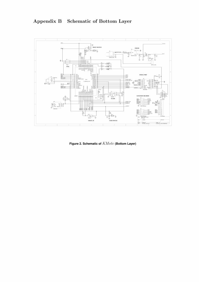
Appendix B Schematic of Bottom Layer
1
1
2
2
3
3
4
4
5
5
6
6
D D
C C
B B
A A
Title
Number RevisionSize
B
Date: 02-May-07 Sheet of File: D:\Thesis\..\micro.sch Drawn By:
S4Toggle Switch
C18
0.1u
DVcc1
P6.3/A32
P6.4/A43
P6.5/A54
P6.6/A6/DAC05
P6.7/A7/DAC1/SVSIN6
Vref+7
XIN8
XOUT/TCLK9
VeREF+10
Vref-/VeREF-11
P1.0/TACLK12
P1.1/TA0/BSLTX13
P1.2/TA114
P1.3/TA215
P1.4/SMCLK16
P1.5
/TA
017
P1.6
/TA
118
P1.7
/TA
219
P2.0
/AC
LK
20
P2.1
/TA
INC
LK21
P2.2
/CA
OU
T/T
A0/
BSL
RX
22
P2.3
/CA
0/TA
123
P2.4
/CA
1/TA
224
P2.5
/Ros
c25
P2.6
/AD
C12
CL
K/D
MA
E026
P2.7
/TA
027
P3.0
/STE
028
P3.1
/SIM
O0/
SDA
29
P3.2
/SO
MI0
30
P3.3
/UC
LK
0/SC
L31
P3.4
/UT
XD
032
P3.5/URXD0 33P3.6/UTXD1 34P3.7/URXD1 35P4.0/TB0 36P4.1/TB1 37P4.2/TB2 38P4.3/TB3 39P4.4/TB4 40P4.5/TB5 41P4.6/TB6 42P4.7/TBCLK 43P5.0/STE1 44P5.1/SIMO1 45P5.2/SOMI1 46P5.3/UCLK1 47P5.4/MCLK 48
P5.5
/SM
CL
K49
P5.6
/AC
LK
50P5
.7/T
Bou
tH/S
VSO
UT
51X
T2O
UT
52X
T2IN
53T
DO
/TD
I54
TD
I55
TM
S56
TC
K57
RST
/NM
I58
P6.0
/A0
59P6
.1/A
160
P6.2
/A2
61A
Vss
62D
Vss
63A
Vcc
64MCU
TI_MSP430_F1611
U5
MSP430
I/O1 Vcc 2
GND 3
U11
DS2411
R172.2k
R14
5.1M
RADIO_RESETRADIO_VREF_EN
RADIO_CSRADIO_SFD
UART1RX
PKT_INT
P_DVCCRADIO_GIO0RADIO_GIO1
R13
470
D5Red LED
R12
220
D4Green LED
R11
100
D3Yellow LED
UART1TX
RADIO_SCLKRADIO_SORADIO_SI
C24
0.1u
1 122
3 344
5 566
7 788
U4
JTAG
DVCC
R7
47k
RESET
R18470k
C250.1u
L5
F Bead Isolator C26
1u Vout 2
GND 3
Vin1
U2
MCP1700_3302C27
1uR810k
D1
Schottky
+1
-2
D2
BATT_CONN
P_DVCC
C190.1u
DVCC
Unregulated Supply
12345
6789
J1
RS232
S1SW-PB
S2
SW-PB
POWER
FLASH
JTAG
SERIAL ID USER SWITCH
SERIAL PORT
RESET SWITCH
1
2
3-
+
S3
POWR_CONN
ADC4ADC5DAC0_ADC6SVSin_ADC7
GIO
1G
IO2
GIO
3G
IO4
GIO
5
GIO
6G
IO7
GIO
8
UA
RT
0TX
I2C
SD
A
I2C
SC
L
UART0RX
GIO13
GIO9GIO10GIO11GIO12
SVSo
ut
AD
C0
AD
C1
AD
C2
USERINT
AVCC
AVCCADC4ADC5DAC0_ADC6SVSin_ADC7
GIO1GIO2UART0RXUART0TXRADIO_GIO1GIO3
AVCCADC0ADC1ADC2GIO4
I2C SCLI2C SDAUSERINTRESET
SVSout GIO6
EXPANSION HEADERS
C17
1u
C1+1
V+2
C1-3
C2+4
C2-5
V-6
INVALID7
T1IN8
T2IN9
R2OUT10 R1OUT 11FORCEON 12VL 13R2IN 14R1IN 15T2OUT 16T1OUT 17GND 18FORCEOFF 19VCC 20U6
MAX3380E
C200.1u
C220.1uC230.1u
C210.1u
DVCC
R1947k
D6
Diode
R15
10K
12345678910111213141516
JP2
LCD Display
AVCC
GIO12GIO11GIO10GIO9
GIO8GIO7
GIO6R16
2K
C300.1u
C310.1u
C322.2u
12JP1
C330.1u
R302.2k
P_DVCC
FORCEOFF
FORCEOFF
FORCEON
FORCEON
Vout
Vout
S1
Q2
W3
Vss4 D 5C 6HOLD 7Vcc 8
M25P80
U7
GIO5
GIO13
123456
789
101112
U9
12 PIN_HEADER
1234567
89
1011121314
U8
14PIN_HEADER
123
X2CRSYTAL
KMote_Bottom Layer
Naveen Madabhushi
Vout1
NC2
NC3
GND4 Shutdown 5NC 6NC 7VDD 8
U10
TMP36FSZ
AVCC
UART1RX
IIT Kanpur
Figure 2. Schematic of KMote (Bottom Layer)

Appendix C Procedure to Connect External Antenna to
KMote
Figure 3. Position of capacitors C13 and C14
To connect an external antenna, the path to antenna has to be disconnectedand the output from radio chip has to be connected to the track leading to SMAConnector. To achieve this capacitor C13 has to be de-soldered and soldered onthe pads for capacitor C14. The positions of capacitors C13 and C14 on the moteare shown in in Figure 3. Further, an SMA connector has to be soldered to thefive vias provided on the PCB. The central via connects to the antenna feed whilethe other four vias are connected to ground. A 50 Ω can then be connected to theSMA connector to extend the range of KMote.

Appendix D Steps Involved in Integrating KMote with
TinyOS
In chapter 3, we briefly described the procedure for integrating KMote withTinyOS. In this section, we cover in detail the steps involved in integrating themote. The steps are as enumnerated under:
• Create a new directory for KMote under tos/platforms
• Create a .platform file that contains basic compiler specific information foreach platform.
• The next step is to create a hardware.h file and put it in the same direc-tory as the KMote directory. This file is included by default when com-piling an application for that platform. This file defines platform-specificconstants, pin names, and also include other ”external” header files (e.g.msp430hardware.h)
• Setting up the build environment for KMote. Prior to compiling any appli-cation, it is important for build environment of TinyOS to be aware of aplatform called KMote. The TinyOS build environment is a set of Makerulesand definitions that include invoking necessary compilation commands andincludes support for other important aspects such as device reprogramming.
• Creation of PlatformP and PlatformC files. After letting the build environ-ment know of existence of KMote, it is also necessary to include PlatformPand PlatformC files. The requirement of these files is described in detail inTEP107 [11]. The basic idea to define these files is that these files provideone and only one instance of Init interface.

Appendix E Procedure to load programs on to KMote us-
ing JTAG and gdb
In chapter 4, we mentioned about testing of KMote using JTAG and gdb. Insection, we describe the procedure to do the same in TinyOS. A detailed descriptionon the procedure to setup debugging environment under linux is available at [2].The steps for setting up gdb under Cygwin are as under:
• Prepare a JTAG interface board as per the connection diagram shown inFigure 4.1.
• Download mspgcc-20060502.exe from [6]. This installer has two packages,msp430-gdb and msp430-gdbproxy which are required to setup the debuggingenvironment.
• Carry out a custom installation and uncheck all the boxes except ”Debugger”and ”JTAG and BSL”.
• Copy msp430-gdb and msp430-gdbproxy to MSP430 tools directory.
• If MSPGCC is installed in the default location, then the following commandwill perform the necessary task: cp /cygdrive/c/mspgcc/bin/msp430-gdb*/opt/msp430/bin
• Copy the files HIL.dll and MSP430.dll using the following commands. Thesefiles are needed to interface with TI MSP430FET pod: cp /cygdrive/c/mspgcc/HIL.dll/opt/msp430/bin and cp /cgdrive/c/mspgcc/MSP430.dll /opt/msp430/bin
• Connect the other end of JTAG interface board to TI MSP430FET pod andplug the USB end of the pod to PC. The open a shell and run the followingcommand: msp430-gdbproxy msp430 TIUSB
• If everything works as it should, the rest of the procedure is same as describedat [2]

Bibliography
[1] CC2420 Datasheet. www.chipcon.com/files/CC2420_Data_Sheet_1_3.
pdf.
[2] Debugging with GDB under Linux. http://www.eecs.harvard.edu/~mdw/
proj/tmote-gdb/.
[3] Elfsys. http://www.elfsys.net.
[4] Folded Dipole Antenna for CC2420. http://www.chipcon.com/files/AN_
040_Folded_Dipole_Antenna_for_CC24XX_1_0.pdf.
[5] MAX3380 Transreceiver Datasheet. http://datasheets.maxim-ic.com/en/ds/MAX3380E-MAX3381E.pdf.
[6] MSPGCC. http://sourceforge.net/project/showfiles.php?group_id=
42303.
[7] Schematic of telosb. http://webs.cs.berkeley.edu/tos/hardware/telos/telos-revb-2004-09-27.pdf.
[8] ST M25P80 Flash Datasheet. http://www.st.com/stonline/books/pdf/
docs/8495.pdf.
[9] Temperature Sensor TMP36FSZ Datasheet. http://www.analog.com/
UploadedFiles/Data_Sheets/TMP35_36_37.pdf.
[10] Tiny Node Datasheet. http://www.btnode.ethz.ch/pub/uploads/
Projects/tinynode-datasheet.pdf.
[11] Tinyos TEPs. http://www.tinyos.net/scoop/special/working_group_
tinyos_2-0.
[12] Tmote Sky Datasheet. http://www.moteiv.com/products/docs/
tmote-sky-datasheet.pdf.
[13] Voltage Regulator MCP1700-3302 Datasheet. http://ww1.microchip.com/
downloads/en/DeviceDoc/21826b.pdf.
[14] XE1205 Radio chip Datasheet. http://www.semtech.com/pc/
downloadDocument.do?id=769.
[15] Juang, P., Oki, H., Wang, Y., Martonosi, M., Peh, L. S., andRubenstein, D. Energy-efficient computing for wildlife tracking: designtradeoffs and early experiences with zebranet. In ASPLOS-X: Proceedings ofthe 10th international conference on Architectural support for programminglanguages and operating systems (New York, NY, USA, 2002), ACM Press,
34

pp. 96–107.
[16] Kim, S., Pakzad, S., Culler, D., Demmel, J., Fenves, G., Glaser,S., and Turon, M. Health monitoring of civil infrastructures using wirelesssensor networks. In IPSN ’07: Proceedings of the 6th international conferenceon Information processing in sensor networks (New York, NY, USA, 2007),ACM Press, pp. 254–263.
[17] Krishnamurthy, L., Adler, R., Buonadonna, P., Chhabra, J.,Flanigan, M., Kushalnagar, N., Nachman, L., and Yarvis, M. De-sign and deployment of industrial sensor networks: experiences from a semi-conductor plant and the north sea. In SenSys ’05: Proceedings of the 3rdinternational conference on Embedded networked sensor systems (New York,NY, USA, 2005), ACM Press, pp. 64–75.
[18] Mainwaring, A., Culler, D., Polastre, J., Szewczyk, R., and An-derson, J. Wireless sensor networks for habitat monitoring. In WSNA ’02:Proceedings of the 1st ACM international workshop on Wireless sensor net-works and applications (New York, NY, USA, 2002), ACM Press, pp. 88–97.
[19] Polastre, J., Szewczyk, R., and Culler, D. Telos: enabling ultra-lowpower wireless research. In IPSN ’05: Proceedings of the 4th internationalsymposium on Information processing in sensor networks (Piscataway, NJ,USA, 2005), IEEE Press, p. 48.
[20] Raman, B., Chebrolu, K., Madabhushi, N., Gokhale, D. Y.,Valiveti, P. K., and Jain, D. Implications of link range and (in)stabilityon sensor network architecture. In WiNTECH ’06: Proceedings of the 1stinternational workshop on Wireless network testbeds, experimental evaluation& characterization (New York, NY, USA, 2006), ACM Press, pp. 65–72.
[21] Sheth, A., Tejaswi, K., Mehta, P., Parekh, C., Bansal, R., Mer-chant, S., Singh, T., Desai, U. B., Thekkath, C. A., and Toyama,K. Senslide: a sensor network based landslide prediction aystem. In SenSys’05: Proceedings of the 3rd international conference on Embedded networkedsensor systems (New York, NY, USA, 2005), ACM Press, pp. 280–281.
[22] Szewczyk, R., Mainwaring, A., Polastre, J., Anderson, J., andCuller, D. An analysis of a large scale habitat monitoring application.In SenSys ’04: Proceedings of the 2nd international conference on Embeddednetworked sensor systems (New York, NY, USA, 2004), ACM Press, pp. 214–226.
[23] Tolle, G., Polastre, J., Szewczyk, R., Culler, D., Turner, N.,Tu, K., Burgess, S., Dawson, T., Buonadonna, P., Gay, D., andHong, W. A macroscope in the redwoods. In SenSys ’05: Proceedings ofthe 3rd international conference on Embedded networked sensor systems (NewYork, NY, USA, 2005), ACM Press, pp. 51–63.
[24] Warneke, B., Last, M., Liebowitz, B., and Pister, K. S. J. Smartdust: Communicating with a cubic-millimeter computer. Computer 34, 1(2001), 44–51.
[25] Werner-Allen, G., Lorincz, K., Welsh, M., Marcillo, O., John-

son, J., Ruiz, M., and Lees, J. Deploying a wireless sensor network onan active volcano. IEEE Internet Computing 10, 2 (2006), 18–25.