kelly weiskittel, advisor: dr. dale ewbank
TRANSCRIPT
•Determined spin speeds and times for SOC, BARC, and PR depositions•Deposition rates determined:
•Nitride = ~64 Å/s with 20 min. deposition in LPCVD•Oxide = ~88 Å/s in Applied Materials P5000 TEOS chamber
•Produced the following standard deviations in film uniformity:•SOC: 1.56%•Oxide: 3.45%•BARC: 0.47%•Photoresist: 1.27%•Nitride: 1.49%
•Etch rates determined:•Oxide: ~32 Å/s•BARC: ~8 Å/s•Nitride: ~3 Å/s
13
37th Annual Microelectronic Engineering Conference – Rochester Institute of Technology April 2019
Fabrication of Sub-300nm Fins by Self-Aligned Double Patterning at RITKelly Weiskittel, Advisor: Dr. Dale Ewbank
Rochester Institute of Technology, Department of Electrical and Microelectronic Engineering, Rochester, NY 14623
Project ObjectivesGoal: Fabricate sub-300nm silicon fins at RIT’sSFML by self-aligned double patterning (SADP).
Motivation:• Patterning advancements necessary to uphold
Moore’s Law• SADP FinFETS• RIT currently only has a planar CMOS process
Theory
Process Flow [1]
Conclusions
Acknowledgements
Laboratory Results (continued)
Future Work:• Development of RIE/hardmask plasma etch
process improvements• Develop complete implementation of P5000 tool
cluster• Undergraduate course – implementation of fin
fabrication in labs• PhD candidate – development of finFET process
200 nm 200 nm
References:[1] O'Connell, Christopher, "An Etching Study for Self-Aligned Double Patterning" (2018). Thesis. Rochester Institute of Technology. Accessed fromhttps://scholarworks.rit.edu/theses/9906
RCA CleanSOC HardmaskDepositionOxide Mandrel DepositionBARC DepositionPhotolithographyEtch BARCTrim Etch for MandrelMandrel EtchSolvent StripSilicon Nitride DepositionSilicon Nitride Spacer EtchStrip Oxide MandrelEtch SOCEtch Silicon Fins
• Stephanie Bolster• RIT Microelectronic
Engineering Undergraduate Class of 2019
• Hard mask layer needed on top of oxide mandrel layer
• In addition, oxide mandrel etch may not be anisotropic enough, resulting in undesirable removal of silicon nitride spacers
• Further testing and development necessary• Undergraduate course – implementation of fin
fabrication in labs
• Dr. Pearson• Dr. Ewbank• Christopher O’Connell• RIT SFML Staff• Matthew Hartensveld• Paul Gregorius• Dr. Fuller
12
11
10
9
8
7
6
5
4
3
2
1
Laboratory Results
• SADP allows for the lithography pattern to be transferred to a mandrel, which in turn will be used as an etch mask.
• Smaller features may be realized without the implementation of more expensive lithography equipment.
Silicon Substrate
Spin on Carbon
Oxide
BARC
Nitride
Positive Photoresist
14
13
Patterning of multi-width lines and spaces.
6
7
5
8
9
10 11
12
13
14
•Lithography:•Qualified AZ MiR 701 PR for use with process•Thinned resist 2:1, 701 PR:PGMEA for 300nm coat•FEM performed Conventional illumination, NA = 0.48, Sigma = 0.625 dose = 148 �𝑚𝑚𝑚𝑚
𝑐𝑐𝑚𝑚2
Oxide Mandrel Etch:60 second etch30 scc CHF360 scc CF4100 scc Ar
Wide oxide mandrel on silicon substrate.
Zoomed-in view of oxide mandrel sidewall.
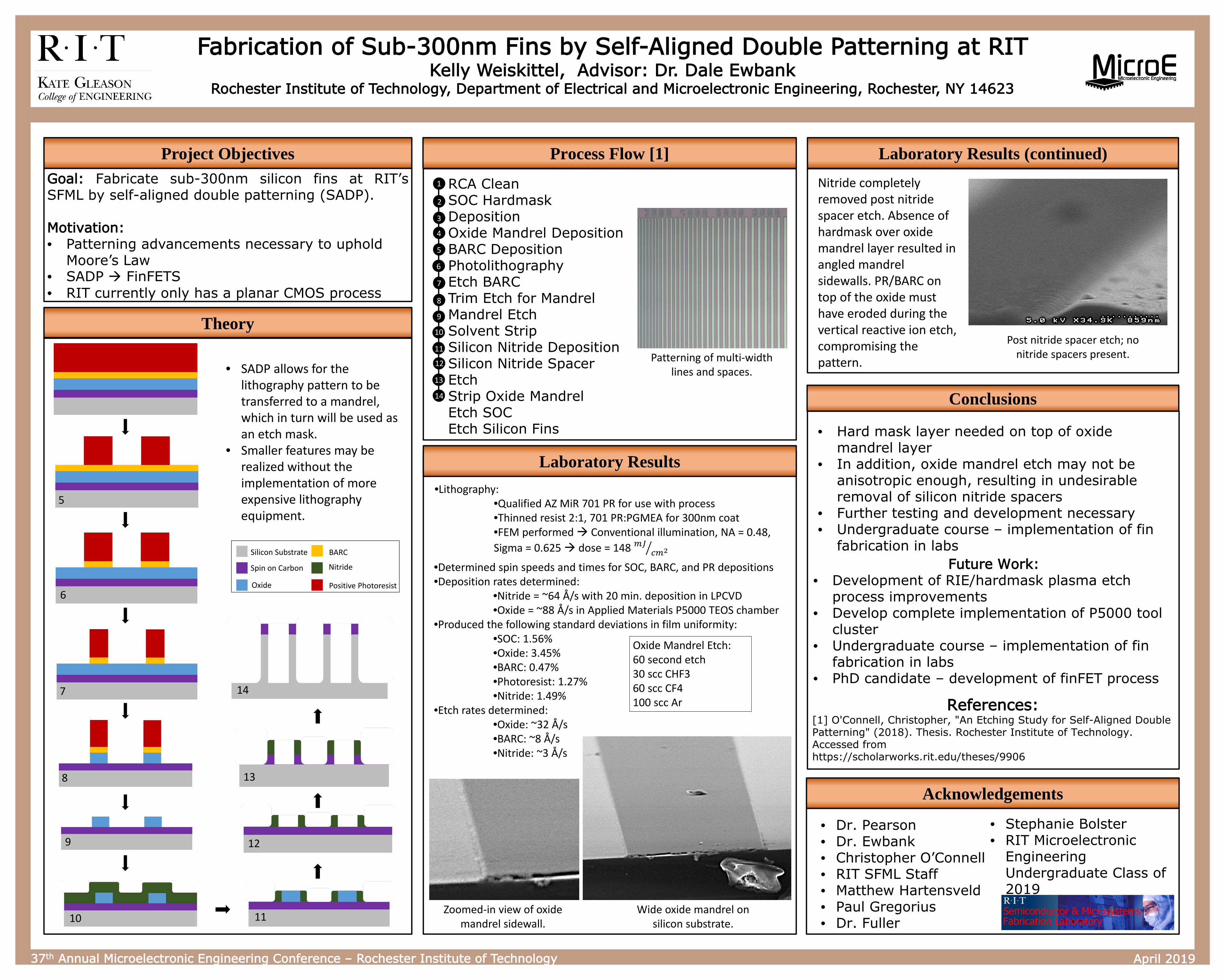
Post nitride spacer etch; no nitride spacers present.
Nitride completely removed post nitride spacer etch. Absence of hardmask over oxide mandrel layer resulted in angled mandrel sidewalls. PR/BARC on top of the oxide must have eroded during the vertical reactive ion etch, compromising the pattern.