jeita workshop, may 20, 2002 alf tutorial wolfgang roethig chairman, ieee p1603 (alf) workgroup...
TRANSCRIPT

JEITA workshop, May 20, 2002
ALF tutorial
Wolfgang RoethigChairman, IEEE P1603 (ALF) WorkgroupSenior Engineering Manager, NEC Electronics

May 20, 2002 www.accellera.org 2
• Motivation for ALF• ALF support in the industry• ALF standardization status• ALF modeling concepts• ALF modeling applications• Conclusion and outlook
Overview

May 20, 2002 www.accellera.org 3
Motivation for ALF
• Complexity of design flows and tools• Multiple views for increasing number of tools
• Expensive library preparation• Frequent version change of too-specific libraries
• Advantages of standard library description• Reduced cost• Increased quality• Resource and time saving for library creation and validation• Facilitate tool interoperability• Leverage 3rd party library sources• Anticipate technology innovations
May 20, 2002 www.accellera.org 4
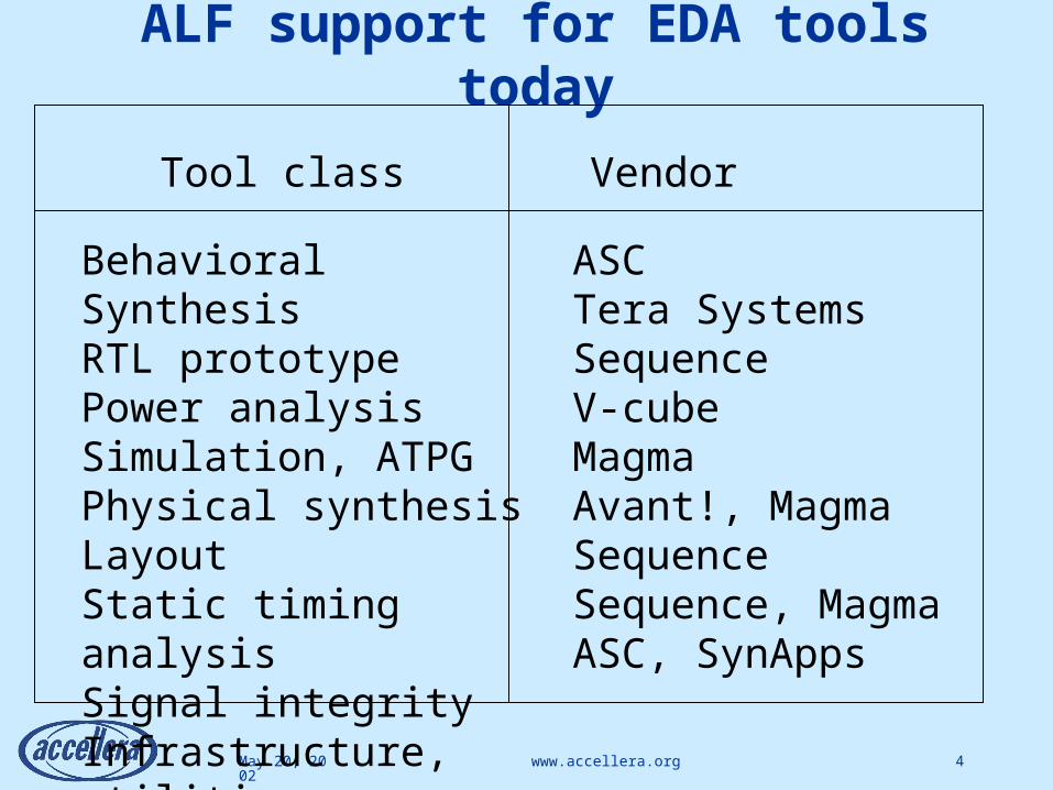
ALF support for EDA tools today
Tool class Vendor
Behavioral SynthesisRTL prototypePower analysisSimulation, ATPGPhysical synthesisLayoutStatic timing analysisSignal integrityInfrastructure, utilities
ASCTera SystemsSequenceV-cubeMagmaAvant!, MagmaSequenceSequence, MagmaASC, SynApps

May 20, 2002 www.accellera.org 5
ALF support for libraries today
Category Vendor
ASIC vendor
EDA tool user
IP library
Characterization tool
Infineon, NEC, Philips
Agere, Intel, Motorola
ARM, Artisan, NurLogic, Virtual Silicon
LibTech, Silicon Metrics
May 20, 2002 www.accellera.org 6
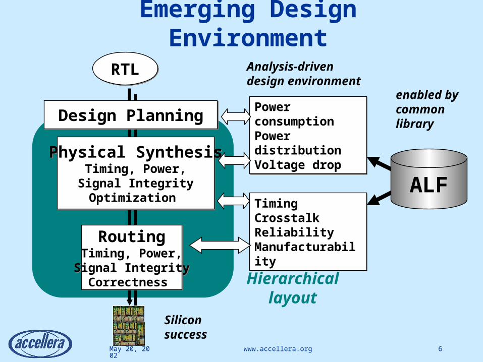
Hierarchicallayout
Emerging Design Environment
RTLRTL
Physical SynthesisTiming, Power,Signal IntegrityOptimization
Physical SynthesisTiming, Power,Signal IntegrityOptimization
RoutingTiming, Power,Signal Integrity
Correctness
RoutingTiming, Power,Signal Integrity
Correctness
Design PlanningDesign Planning
TimingCrosstalkReliabilityManufacturability
TimingCrosstalkReliabilityManufacturability
Power consumptionPowerdistributionVoltage drop
Power consumptionPowerdistributionVoltage drop
Analysis-drivendesign environment
ALF
enabled bycommonlibrary
Siliconsuccess
May 20, 2002 www.accellera.org 7
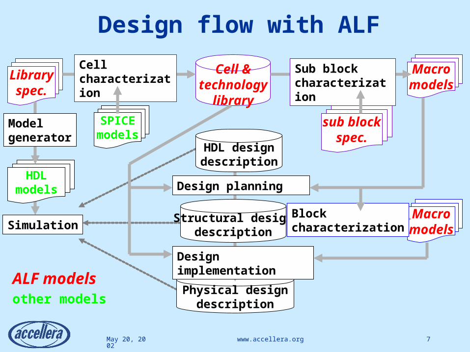
Design flow with ALF
Simulation
ALF modelsother models
Libraryspec.
HDLmodels
Modelgenerator
Physical designdescription
HDL designdescription
Structural designdescription
Design planning
Design implementation
Cell &technology
library
Cell characterization
SPICEmodels
Macromodels
Sub blockcharacterization
sub blockspec.
Macromodels
Blockcharacterization

May 20, 2002 www.accellera.org 8
ALF standardization status• Started as OVI workgroup in 1996
• Initial members: Avant!, Cadence, LSI Logic, Mentor Graphics, ViewLogic, VLSI
• Version 1.0 approved as OVI standard e/o 1997• covers function, timing, power
• OVI successor organization Accellera endorsed ALF• Version 2.0 approved as Accellera standard e/o 2000
• added signal integrity, interconnect analysis and layout
• IEEE P1603 workgroup started in 2001• Today’s members:
ASC, Infineon, Magma, Mentor Graphics, Monterey, NEC, Philips, Sequence, Simplex, Sun Microsystems, Tera Systems
• IEEE P1603 ballot scheduled for 2H of 2002• Joint ballot with IEC planned

May 20, 2002 www.accellera.org 9
ALF scope defined in IEEE PAR
• ALF shall serve as the data specification of library elements for design applications used to implement integrated circuits. The range of abstraction shall include from the register-transfer level (RTL) to the physical implementation level.
• The language shall model behavior, timing, power, signal integrity, physical abstraction and physical implementation rules of library elements.

May 20, 2002 www.accellera.org 10
ALF scope illustrated
Timing Power
Signal integrity
Electrical model
Simulation
Formal verification Design for test
Synthesis
Functional model
LayoutInterconnect
Hierarchical abstraction
Physical modelUnified ALF
library

May 20, 2002 www.accellera.org 11
ALF data model LIBRARY SUBLIBRARY
CELL
PIN
Functional domain
FUNCTION
PRIMITIVE
PIN
TEST
VECTOR
WIRE
NODEArithmetic model
Electrical domain
PORT
BLOCKAGE
Physical domain
PATTERN
Geometric model
Arithmetic model
LAYER
VIA
RULE
SITE
ANTENNA
REGION

May 20, 2002 www.accellera.org 12
ALF modeling concepts
• Modeling foundation concepts• Arithmetic model concept
> Electrical and physical library data description
• VECTOR concept> Stimulus for function, timing, electrical characterization
• Higher-level modeling concepts• FUNCTION, TEST
> Canonical description of functional behavior> Interface between tester algorithm and DUT
• TEMPLATE, GROUP> Re-usable definitions> Description of parametrizable IP blocks
Covered by this tutorial
Covered by other tutorial [CICC2001]
May 20, 2002 www.accellera.org 13
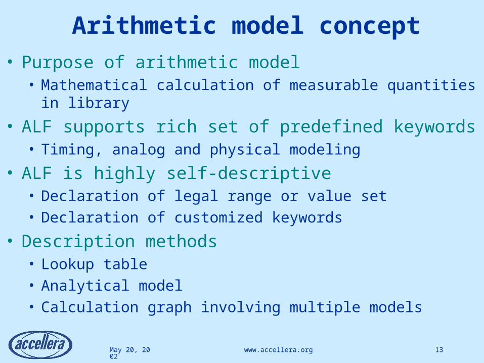
Arithmetic model concept
• Purpose of arithmetic model• Mathematical calculation of measurable quantities in library
• ALF supports rich set of predefined keywords• Timing, analog and physical modeling
• ALF is highly self-descriptive• Declaration of legal range or value set• Declaration of customized keywords
• Description methods• Lookup table• Analytical model• Calculation graph involving multiple models

May 20, 2002 www.accellera.org 14
Predefined arithmetic models (1 of 2)
Timing
Analog
DELAY, RETAIN, SLEWRATE, SKEW, JITTER, SETUP, HOLD, RECOVERY, REMOVAL, PULSEWIDTH, PERIOD, ILLEGAL, NOCHANGE, THRESHOLD, NOISE, NOISE_MARGIN
VOLTAGE, CURRENT, TIME, FREQUENCY, CAPACITANCE, RESISTANCE, INDUCTANCE, ENERGY, POWER, FLUX, FLUENCE,TEMPERATURE
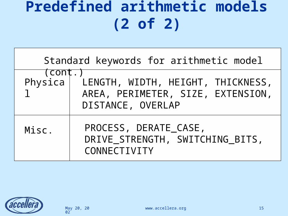
Standard keywords for arithmetic model
May 20, 2002 www.accellera.org 15
Predefined arithmetic models (2 of 2)
Physical
Misc.
LENGTH, WIDTH, HEIGHT, THICKNESS,AREA, PERIMETER, SIZE, EXTENSION, DISTANCE, OVERLAP
PROCESS, DERATE_CASE, DRIVE_STRENGTH, SWITCHING_BITS, CONNECTIVITY
Standard keywords for arithmetic model (cont.)
May 20, 2002 www.accellera.org 16
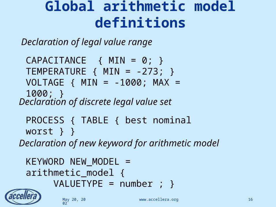
Global arithmetic model definitions
KEYWORD NEW_MODEL = arithmetic_model {VALUETYPE = number ; }
CAPACITANCE { MIN = 0; }TEMPERATURE { MIN = -273; }VOLTAGE { MIN = -1000; MAX = 1000; }
PROCESS { TABLE { best nominal worst } }
Declaration of legal value range
Declaration of discrete legal value set
Declaration of new keyword for arithmetic model

May 20, 2002 www.accellera.org 17
Arithmetic model with TABLE
CAPACITANCE {HEADER {
TEMPERATURE { TABLE { 0 70 125 } }VOLTAGE { TABLE { 0.5 1.5 } }PROCESS { TABLE { best nominal worst } }
} TABLE { 9.8 10.0 9.9 10.2 12.0 11.5 8.5 8.9 8.8 9.5 10.0 9.7 7.8 8.1 7.9 8.7 9.3 8.9
} }
3rd point in 1st dimension1st point in 2nd dimension2nd point in 3rd dimensionPROCESS = nominal
VOLTAGE = 0.5TEMPERATURE = 125CAPACITANCE = 8.8
applies for
Example for 3-D lookup table

May 20, 2002 www.accellera.org 18
Arithmetic model with EQUATION
CAPACITANCE {HEADER {
TEMPERATURE Ta { /* no table */ }VOLTAGE Vc { /* no table */ }PROCESS { /* no table */ }
} EQUATION {(PROCESS==best)? ( 10.0 + 0.01*(Vc + 0.2*Ta) ) :(PROCESS==nominal)? ( 9.8 + 0.02*(Vc + 0.1*Ta) ) :(PROCESS==worst)? ( 9.5 + 0.025*(Vc + 0.15*Ta) ) :-1
} }
Example for 3-D analytical model

May 20, 2002 www.accellera.org 19
Arithmetic model with reference
TEMPERATURE temp1 {HEADER { NEW_MODEL { TABLE { … } } } TABLE { … } }
CAPACITANCE {HEADER {
TEMPERATURE { MODEL=temp1; TABLE { … } }VOLTAGE { TABLE { … } }PROCESS { TABLE { … } }
} TABLE { … } }
Example for calculation graph
Data for NEW_MODEL
calculate TEMPERATURE
Data for PROCESSData for VOLTAGE
calculate CAPACITANCE
Primary input data
Primary input data
Primary input data

May 20, 2002 www.accellera.org 20
VECTOR concept
• Purpose of Vector• Describe stimulus for electrical characterization• Describe functional waveform• Describe trigger for sequential behavior
• Description methods• Boolean expression for static state• Vector expression for temporal behavior

May 20, 2002 www.accellera.org 21
Single-Event Vector Expressions
Vector expressionTiming diagram for a signal A
(01 A)
(0? A)
(?1 A)
(?! A)
(0* A)
(*1 A)
(?* A)
(*? A)
May 20, 2002 www.accellera.org 22
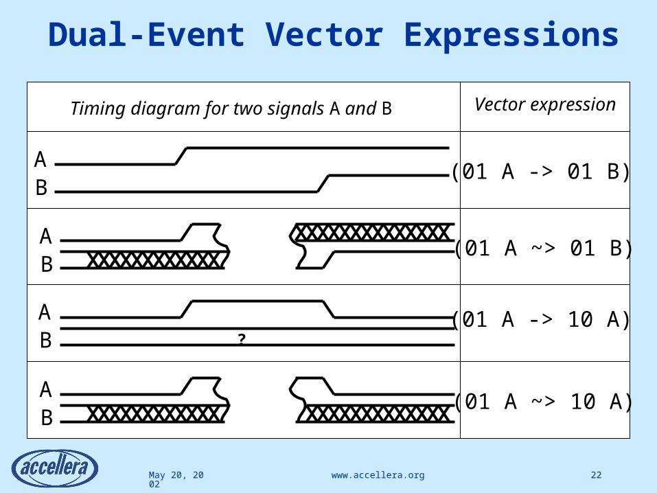
Dual-Event Vector Expressions
Vector expressionTiming diagram for two signals A and B
(01 A -> 01 B)AB
(01 A ~> 01 B)AB
(01 A -> 10 A)AB
AB
(01 A ~> 10 A)
?

May 20, 2002 www.accellera.org 23
Conditional Vector Expressions
Vector expressionTiming diagram for two signals A and B
(01 A & 01 B)
(01 A & B)
AB
AB == 1
Logical condition
Simultaneous switching
May 20, 2002 www.accellera.org 24
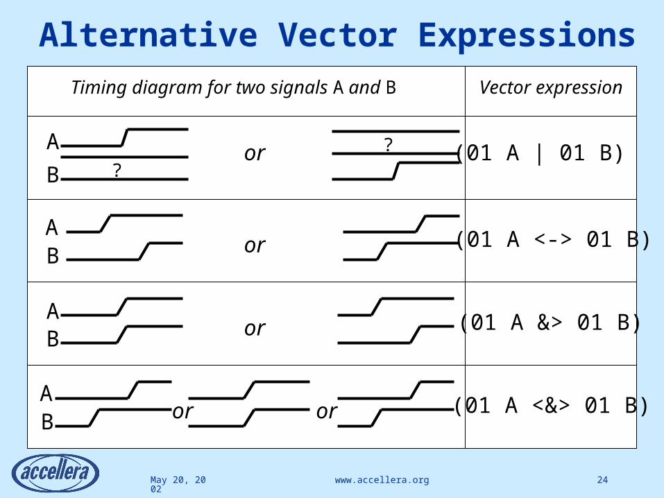
Alternative Vector Expressions Vector expressionTiming diagram for two signals A and B
(01 A <-> 01 B)
(01 A <&> 01 B)
AB
AB or or
or
A
B ??or (01 A | 01 B)
AB or (01 A &> 01 B)

May 20, 2002 www.accellera.org 25
ALF Modeling applications• Cell modeling
• Timing modeling• Power modeling
• Interconnect modeling• Distributed load, boundary parasitics• Interconnect delay, noise
• Signal integrity• Noise
• Reliability• Electromigration
• Manufacturability• Antenna

May 20, 2002 www.accellera.org 26
Example for CELL description
CELL myCell {PIN in1 { DIRECTION = input; }PIN in2 { DIRECTION = input; }PIN out1 { DIRECTION = output; }FUNCTION {
BEHAVIOR { out1 = in1 & in2; }}VECTOR (01 in1 -> 01 in2) {
DELAY { FROM { PIN = in1; } TO { PIN = in2; }HEADER {
CAPACITANCE cload { PIN = in2; }SLEWRATE trise { PIN = in1; }
} EQUATION { 0.3 + cload*(0.2 + 0.1*trise) } }
} // put other models, e.g. ENERGY, NOISE etc.}

May 20, 2002 www.accellera.org 27
Timing modeling
• ALF supports DELAY and SLEWRATE with THRESHOLD definition per timing arc• Optimal THRESHOLD can be chosen for characterization• Library data matches SPICE characterization data
• ALF supports driver RESISTANCE• Accurate waveform at driver output• Accurate calculation of effective capacitance• Better accuracy for cell and interconnect delay
• ALF supports standard timing checks• SETUP, HOLD, RECOVERY, REMOVAL, SKEW• MIN, MAX LIMIT for PULSEWIDTH, PERIOD

May 20, 2002 www.accellera.org 28
DELAY• Timing arc specification in VECTOR• PIN and THRESHOLD definition in FROM, TO• THRESHOLD per library, per pin, or per arc
DELAY
THRESHOLD
THRESHOLD
VECTOR ( 01 in1 -> 10 out1 ) {DELAY {
FROM { PIN=pin1; THRESHOLD = 0.5; }TO { PIN=pin0; THRESHOLD = 0.4; }
} }
rising edge falling edge

May 20, 2002 www.accellera.org 29
SLEWRATE• Timing arc specification in VECTOR• THRESHOLD definition in FROM, TO• THRESHOLD per library or per arc
SLEWRATE
THRESHOLD
THRESHOLD
VECTOR ( 01 in1 -> 10 out1 ) {SLEWRATE { PIN = out1;
FROM { THRESHOLD = 0.6; }TO { THRESHOLD = 0.3; }
} }

May 20, 2002 www.accellera.org 30
Driver RESISTANCE (1 of 2)• Linear SLEWRATE not accurate• Driver RESISTANCE for realistic waveform• Driver model for calculation of effective capacitance
SLEWRATE
THRESHOLD
THRESHOLD
idealized waveform
virtual sourcewaveform
real waveform
Driver model
virtualsource
RESISTANCEeffective capacitance
May 20, 2002 www.accellera.org 31
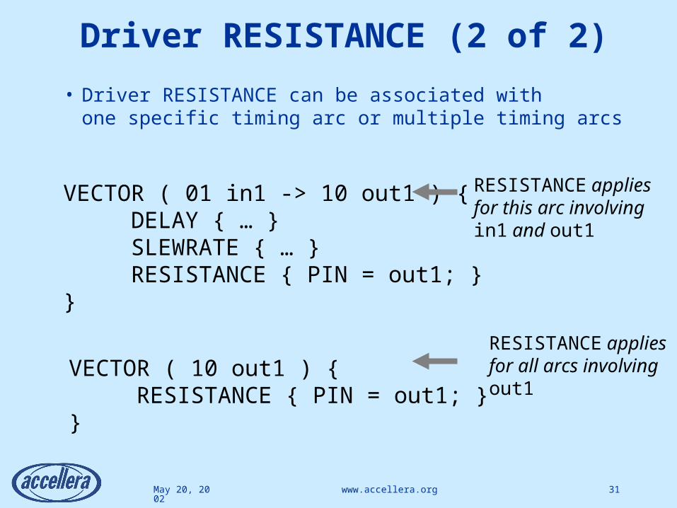
Driver RESISTANCE (2 of 2)
• Driver RESISTANCE can be associated with one specific timing arc or multiple timing arcs
VECTOR ( 01 in1 -> 10 out1 ) {DELAY { … }SLEWRATE { … }RESISTANCE { PIN = out1; }
}
VECTOR ( 10 out1 ) {RESISTANCE { PIN = out1; }
}
RESISTANCE appliesfor this arc involvingin1 and out1
RESISTANCE appliesfor all arcs involvingout1

May 20, 2002 www.accellera.org 32
Timing accuracy• ALF enables more accurate delay calculation• Better correlation with SPICE
Error criterionAverageStd deviationMax - Min
.lib+ 3.9 %+/- 5.0 % 17.4 %
ALF+ 0.5 %+/- 2.2 % 11.1 %
Del ay correl ati on wi th ALF
0.0
0.5
1.0
1.5
2.0
2.5
3.0
3.5
4.0
0.0 0.5 1.0 1.5 2.0 2.5 3.0 3.5 4.0
SPICE [nsec]
Phys
ical
Stu
dio
[nse
c]
ALF
Del ay correl ati on wi th . l i b
0.0
0.5
1.0
1.5
2.0
2.5
3.0
3.5
4.0
4.5
0.0 0.5 1.0 1.5 2.0 2.5 3.0 3.5 4.0
SPICE [nsec]
Phys
ical
Stu
dio
[nse
c]
Conventionaltiming library

May 20, 2002 www.accellera.org 33
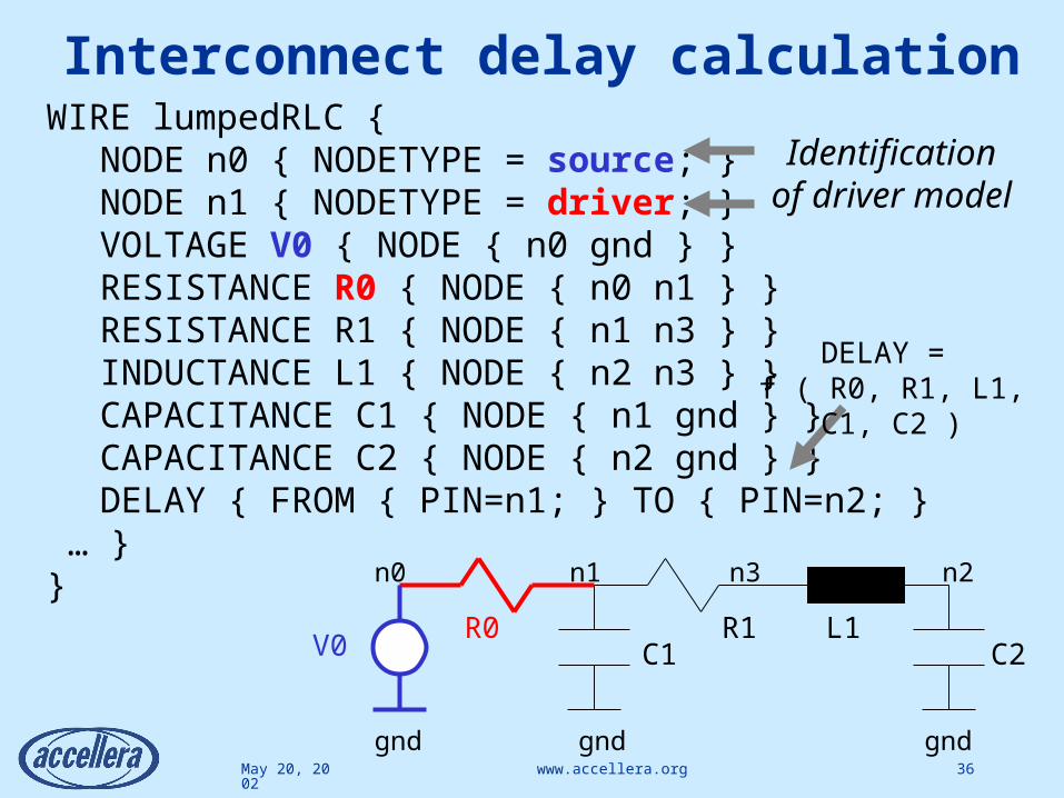
Interconnect modeling
• ALF support distributed load• Characterize cell delay with R,C load• More accurate than lumped capacitance
• ALF supports boundary parasitics• Describe boundary parasitics as R, C• Can include coupling capacitance between pins• More accurate than lumped pin capacitance• Also in conjunction with “donut” model for complex block
• ALF supports interconnect analysis • Interconnect delay calculation• Interconnect noise calculation

May 20, 2002 www.accellera.org 34
Distributed load WIRE pi_load {
NODE n1 { NODETYPE=interconnect; }NODE gnd { NODETYPE=ground; }RESISTANCE R1 { NODE { n1 n2 } }CAPACITANCE C1 { NODE { n1 gnd } }CAPACITANCE C2 { NODE { n2 gnd } }
}
R1n2n1
gndgnd
C1 C2
DELAY { FROM { PIN=pin1; } TO { PIN=pin0; } pi_load w1 { n1 = pin0; }HEADER {
CAPACITANCE c_near { MODEL = w1.C1; }CAPACITANCE c_far { MODEL = w1.C2; }RESISTANCE r_wire { MODEL = w1.R1; }
} EQUATION { … } }
Wire declaration
Wire instantiation
May 20, 2002 www.accellera.org 35
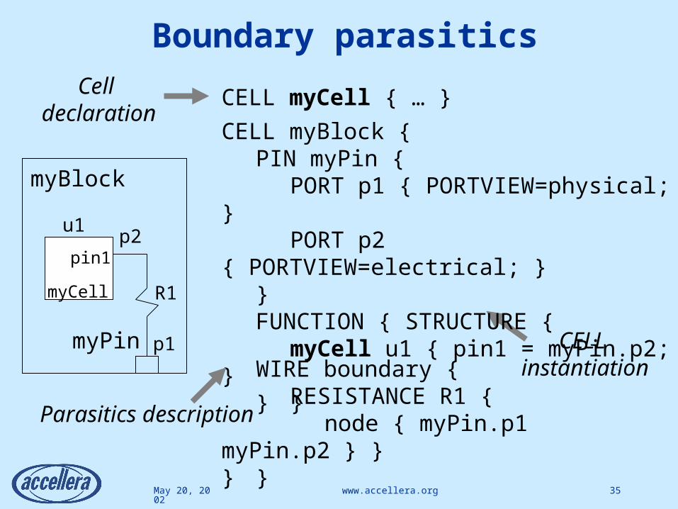
Boundary parasitics
CELL myCell { … }
myBlock
myPin
myCell
u1
pin1p2
p1
R1
Cell declaration
CELL instantiation
CELL myBlock {PIN myPin {
PORT p1 { PORTVIEW=physical; }PORT p2 { PORTVIEW=electrical; }
}FUNCTION { STRUCTURE {
myCell u1 { pin1 = myPin.p2; }} }
WIRE boundary {RESISTANCE R1 {
node { myPin.p1 myPin.p2 } }} }
Parasitics description
May 20, 2002 www.accellera.org 36
Interconnect delay calculation WIRE lumpedRLC {
NODE n0 { NODETYPE = source; }NODE n1 { NODETYPE = driver; }VOLTAGE V0 { NODE { n0 gnd } }RESISTANCE R0 { NODE { n0 n1 } }RESISTANCE R1 { NODE { n1 n3 } }INDUCTANCE L1 { NODE { n2 n3 } }CAPACITANCE C1 { NODE { n1 gnd } }CAPACITANCE C2 { NODE { n2 gnd } }DELAY { FROM { PIN=n1; } TO { PIN=n2; } … }
}
Identificationof driver model
R1
n2n1
gndgnd
C1 C2L1
V0R0
n0
gnd
n3
DELAY = f ( R0, R1, L1, C1, C2 )

May 20, 2002 www.accellera.org 37
Interconnect noise calculation
WIRE lumpedRLC {NODE n0 { NODETYPE = source; }NODE n1 { NODETYPE = driver; }NODE n2 { NODETYPE = receiver; }VOLTAGE V0 { NODE { n0 gnd } }CAPACITANCE C1 { NODE { n0 n1 } }RESISTANCE R1 { NODE { n1 gnd } }RESISTANCE R2 { NODE { n1 n2 } }CAPACITANCE C2 { NODE { n2 gnd } }NOISE { PIN=n2; … }
}
Aggressor
NOISE = f ( V0, C1, R1, R2, C2 )
R2
n2n1
gndgnd
C1 C2V0 R1
n0
gnd
Victim
May 20, 2002 www.accellera.org 38
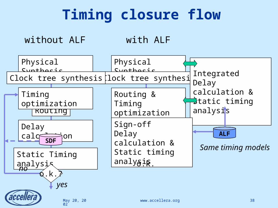
Timing closure flow
Physical Synthesis
Clock tree synthesisIntegratedDelay calculation &Static timing analysisRouting &
Timing optimization
Sign-off Delay calculation &Static timing analysis
Same timing models
ALF
o.k.
with ALF
Physical Synthesis
Clock tree synthesis
Delay calculation
Routing
Timing optimization
SDF
Static Timing analysis
o.k.?
without ALF
yes
no

May 20, 2002 www.accellera.org 39
Power modeling
• ALF supports VECTOR-specific ENERGY & POWER• Most flexible modeling approach• Allows tradeoff between VECTOR set and accuracy
• ALF is complemented by Global Activity File (GAF)• GAF annotates design-specific VECTOR activity• GAF is an emerging industry standard
• ALF supports multiple voltage domains• Association between power supply pin and power rail system• Association between energy and power rail system

May 20, 2002 www.accellera.org 40
ENERGY and POWER
• ENERGY associated with transient VECTOR• POWER associated with static VECTOR
VECTOR ( ( 01 in1 -> 10 out1) && ( ! in2 ) ) {ENERGY { … }
}
VECTOR ( ! in1 && ! in2 ) {POWER { … }
} Static power
Transient energy
Event sequence Logical condition
Logical condition

May 20, 2002 www.accellera.org 41
Power analysis flow (1 of 2)• For each cell instance in design:
• Calculate ENERGY or POWER for each VECTOR• Get frequency or probability or each VECTOR
• Global Activity File (GAF) contains instance-specific frequency or probability for VECTOR• More accurate than frequency and probability per net• Logical correlations are preserved• Exact power results in conjunction with ALF library
ALF GAF
ENERGY(VECTOR) * frequency(VECTOR)
POWER(VECTOR) * probability(VECTOR)
All transient vectors
All static vectors
Total power =
+
May 20, 2002 www.accellera.org 42
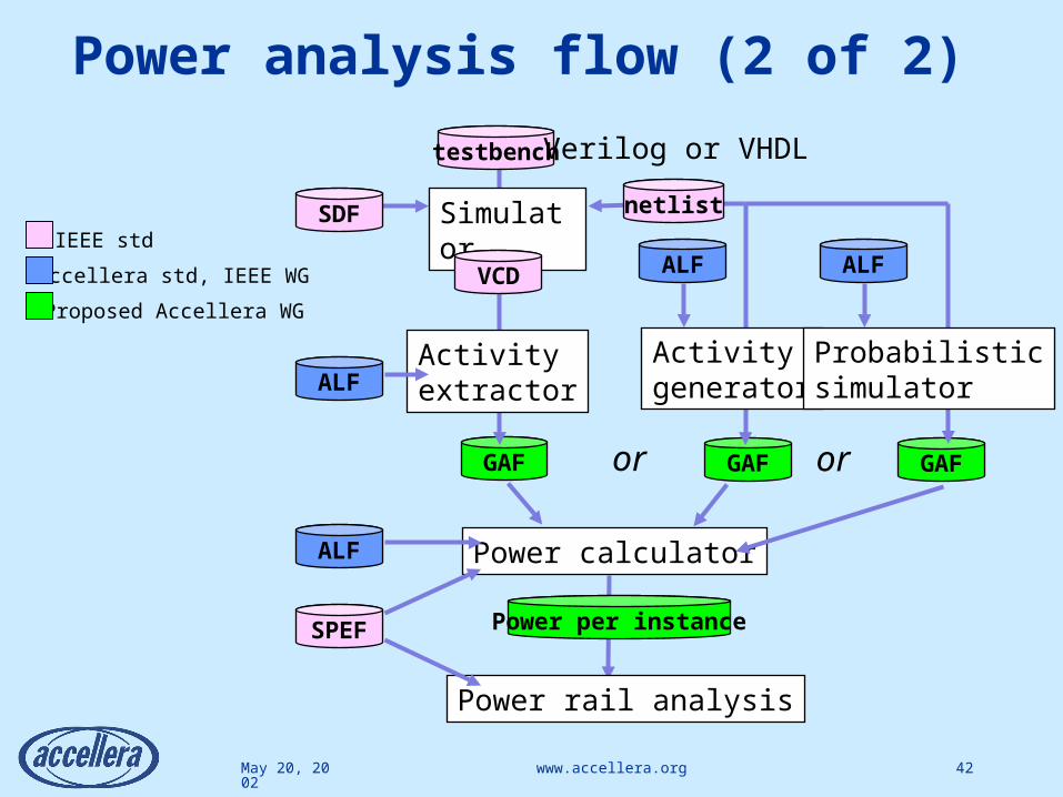
Power analysis flow (2 of 2)
IEEE std
Accellera std, IEEE WG
Proposed Accellera WG
Power rail analysis
Power calculator
Power per instanceSPEF
ALF
GAF
Activitygenerator
or
ALF
GAF
Probabilisticsimulator
or
ALF
GAF
Simulator
Activityextractor
VCD
ALF
netlist
testbench
SDF
Verilog or VHDL

May 20, 2002 www.accellera.org 43
Multiple voltage domains (1 of 2)• Define a CLASS for a power supply system• Define another CLASS for a power rail• Power rail refers to power supply system
CLASS vdd1 { SUPPLY_CLASS = supply1; SUPPLYTYPE = power; VOLTAGE = 1.5; }
CLASS vdd2 { SUPPLY_CLASS = supply2; SUPPLYTYPE = power; VOLTAGE = 1.0; }
CLASS vss { SUPPLY_CLASS { supply1 supply2 } SUPPLYTYPE = ground; }
Common groundfor both supplies
CLASS supply1 { USAGE = SUPPLY_CLASS; }CLASS supply2 { USAGE = SUPPLY_CLASS; }

May 20, 2002 www.accellera.org 44
Multiple voltage domains (2 of 2)• Power/ground pin is connected to power rail • Signal pin refers to power supply system• Energy consumption refers to power supply system
CELL LevelShifter {PIN vdd_15 { CONNECT_CLASS = vdd1 ; }PIN vdd_10 { CONNECT_CLASS = vdd2 ; }PIN vss { CONNECT_CLASS = vss ; }PIN in { DIRECTION=input; SUPPLY_CLASS=supply2; }
PIN out { DIRECTION=output; SUPPLY_CLASS=supply1; }VECTOR (?! in -> ?! out ) {
ENERGY = 0.8 { SUPPLY_CLASS=supply1; }ENERGY = 0.3 { SUPPLY_CLASS=supply2; }
} }
May 20, 2002 www.accellera.org 45
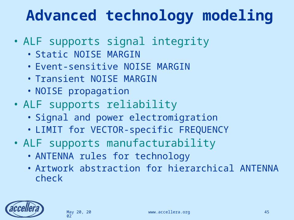
Advanced technology modeling
• ALF supports signal integrity• Static NOISE MARGIN• Event-sensitive NOISE MARGIN• Transient NOISE MARGIN• NOISE propagation
• ALF supports reliability• Signal and power electromigration• LIMIT for VECTOR-specific FREQUENCY
• ALF supports manufacturability• ANTENNA rules for technology• Artwork abstraction for hierarchical ANTENNA check

May 20, 2002 www.accellera.org 46
Static NOISE MARGIN• Static NOISE MARGIN in context of a PIN• Can be specified as LOW and HIGH• NOISE MARGIN is normalized to voltage swing
Voltage swing
High noise margin
Low noise margin
CELL FlipFlop {PIN clk {DIRECTION = input; SIGNALTYPE = clock;
NOISE_MARGIN { LOW=0.4; HIGH=0.3; } }PIN din { DIRECTION = input; SIGNALTYPE = data; }PIN dout { DIRECTION = output; SIGNALTYPE = data; }
}

May 20, 2002 www.accellera.org 47
Event-sensitive NOISE MARGIN
• Event-sensitive NOISE MARGIN in context of a VECTOR• Event is described in VECTOR• Example: noise on data pin during triggering clock edge
VECTOR ( 0* din -> 01 clk -> *0 din ) {NOISE_MARGIN = 0.4 { PIN = din; }
}
NOISE MARGIN
Sensitizing event

May 20, 2002 www.accellera.org 48
Transient NOISE MARGIN• Transient NOISE MARGIN in context of a VECTOR• Depends on PULSEWIDTH of noise waveform
VECTOR ( ( 0* clk -> *0 clk ) && ( din != dout ) ) {NOISE_MARGIN { PIN = clk;
HEADER {PULSEWIDTH { PIN=clk; TABLE { … } } }
TABLE { … } } }
PULSEWIDTH
NOISE MARGIN
static noise margin
NOISE
PULSEWIDTH
Noise event Logical condition

May 20, 2002 www.accellera.org 49
NOISE propagation• NOISE at output pin depends on NOISE at input pin• NOISE propagation arc in context of VECTOR
VECTOR ( 0* pin1 -> *0 pin1 <&> 1* pin0 -> *1 pin0 ) {NOISE { PIN = pin0;
HEADER {NOISE { PIN = pin1; TABLE { … } }PULSEWIDTH { PIN = pin1; TABLE { … } }CAPACITANCE { PIN = pin0; TABLE { … } }
} TABLE { … } } }
NOISE
PULSEWIDTH
NOISE
PULSEWIDTH
DELAY
May 20, 2002 www.accellera.org 50
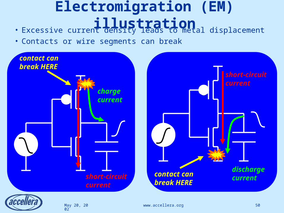
Electromigration (EM) illustration• Excessive current density leads to metal displacement• Contacts or wire segments can break
charge current
discharge currentshort-circuit
current
short-circuit current
contact can break HERE
contact can break HERE

May 20, 2002 www.accellera.org 51
EM rules for technology (1 of 2)• LIMIT for CURRENT described in context of LAYER• Average measurement for DC (power route)• Absolute average measurement for AC (signal route)• Peak and RMS measurement also supported
LAYER metal1 {LIMIT {
CURRENT i_dc { MAX { … } MEASUREMENT = average; }
CURRENT i_ac { MAX { … } MEASUREMENT = absolute_average; }
CURRENT i_peak { MAX { … } MEASUREMENT = peak; }
} }
for power route
for signal route
May 20, 2002 www.accellera.org 52
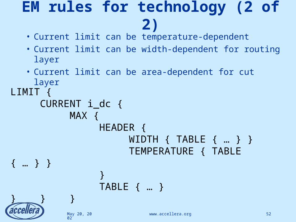
EM rules for technology (2 of 2)• Current limit can be temperature-dependent• Current limit can be width-dependent for routing layer• Current limit can be area-dependent for cut layer
LIMIT {CURRENT i_dc {
MAX {HEADER {
WIDTH { TABLE { … } }TEMPERATURE { TABLE { … } }
}TABLE { … }
} } }

May 20, 2002 www.accellera.org 53
EM rules for interconnect• Models for peak and RMS current can be precharacterized• Simple example: 1st order interconnect model
CAPACITANCE C1 { NODE { n1 gnd } }RESISTANCE R1 { NODE { n0 n1 } }CURRENT { COMPONENT = R1 ; MEASUREMENT = peak;
HEADER {RESISTANCE { MODEL = R1; }CAPACITANCE { MODEL = C1; }SLEWRATE { PIN = n0; }
} TABLE { … } }
virtualsource
RESISTANCE R1 CAPACITANCE C1
NODE n1NODE n0
NODE gnd

May 20, 2002 www.accellera.org 54
• Idea: Identify paths inside cell subjected to EM• Define orthogonal VECTOR set for activating all paths• Abstract EM rule into LIMIT for VECTOR FREQUENCY
EM rules for cells (1 of 2)
pin2
pin1
pin0
4
5
1
3 2
VECTOR (01 pin0) { /* path 1 */ }
VECTOR (01 pin1 -> 10 pin0){ /* path 2 */ }
VECTOR (10 pin2) { /* path 4 */ }
VECTOR (10 pin2 -> 10 pin0){ /* path 3 */ }
VECTOR (01 pin2) { /* path 5 */ }

May 20, 2002 www.accellera.org 55
EM rules for cells (2 of 2)
• Actual current = f (load CAPACITANCE, FREQUENCY)• Maximum allowed current = f (TEMPERATURE)• Maximum allowed FREQUENCY
= f (load CAPACITANCE, SLEWRATE, TEMPERATURE)
VECTOR (01 pin1 -> 10 pin0) {LIMIT { FREQUENCY { MAX {
HEADER {SLEWRATE { PIN=pin1; TABLE { … } }CAPACITANCE { PIN=pin0; TABLE { … } }TEMPERATURE { TABLE { … } }
} TABLE { … }} } } }

May 20, 2002 www.accellera.org 56
EM summary
• ALF supports comprehensive technology EM rules• ALF supports models for signal current calculation• Calculated current must be checked against EM rules
• ALF supports abstract models for cell EM rules• LIMIT for VECTOR-specific FREQUENCY• Can be dependent on SLEWRATE, load CAPACITANCE,
TEMPERATURE• Can incorporate other lifetime-impacting effects,
such as Hot Carrier, Thermal Instability
• Modeling approach scalable to complex cores• VECTOR paradigm same as for power analysis• Global Activity File (GAF) also usable in EM flow

May 20, 2002 www.accellera.org 57
ANTENNA illustration• Transistor collects charge during etching of metal structures• Cumulative effect can destroy the transistor
Photo res.
Diffusion
Gate oxide
Polysilicon
Via 1
Metal 1
Via 2
Metal 2
Via 3
Metal 3
Transistor
Plasma
Plasma
Plasma

May 20, 2002 www.accellera.org 58
ANTENNA rules for technology (1 of 2)
• Prerequistite for ANTENNA rule description:• Each LAYER must be declared in LIBRARY• Order of LAYER declaration must be manufacturing order• Declaration from bottom to top
LIBRARY myTechnology {LAYER diffusion { LAYERTYPE=reserved; }LAYER poly { LAYERTYPE=reserved; }LAYER cut0 { LAYERTYPE=cut; }LAYER metal1 { LAYERTYPE=routing; }LAYER cut1 { LAYERTYPE=cut; }LAYER metal2 { LAYERTYPE=routing; }// etc.
}

May 20, 2002 www.accellera.org 59
ANTENNA rules for technology (2 of 2)
• Charge density depends on ratio between metal and transistor• The greater the metal area and the smaller the transistor area,
the greater the damage• Diffusion alleviates antenna problem by diverting charge
ANTENNA cumulative_area {SIZE s1 { CALCULATION = incremental;
HEADER {AREA a1 { LAYER = metal1; }AREA a0 { LAYER = poly; }CONNECTIVITY { BETWEEN { metal1 diffusion } }
} EQUATION { CONNECTIVITY? 0.5*a1/a0 : a1/a0 } }// put calculation for other layers hereLIMIT { SIZE { MAX = 1000; } } }

May 20, 2002 www.accellera.org 60
ANTENNA rule evaluation
• Antenna rule checker must account for manufacturing order• Count only top-down connections• Combine poly areas connected top-down
metal1
metal2
poly
AREA a0’ = 20 AREA a0’’ = 30
AREA a1’ = 50 AREA a1’’ = 70
AREA a2 = 120
When metal1 is fabricated: check a1’/a0’ = 50/20 and a1’’/a0’’=70/30When metal2 is fabricated: check a2/(a0’+a0’’) = 120/(20+30)
May 20, 2002 www.accellera.org 61
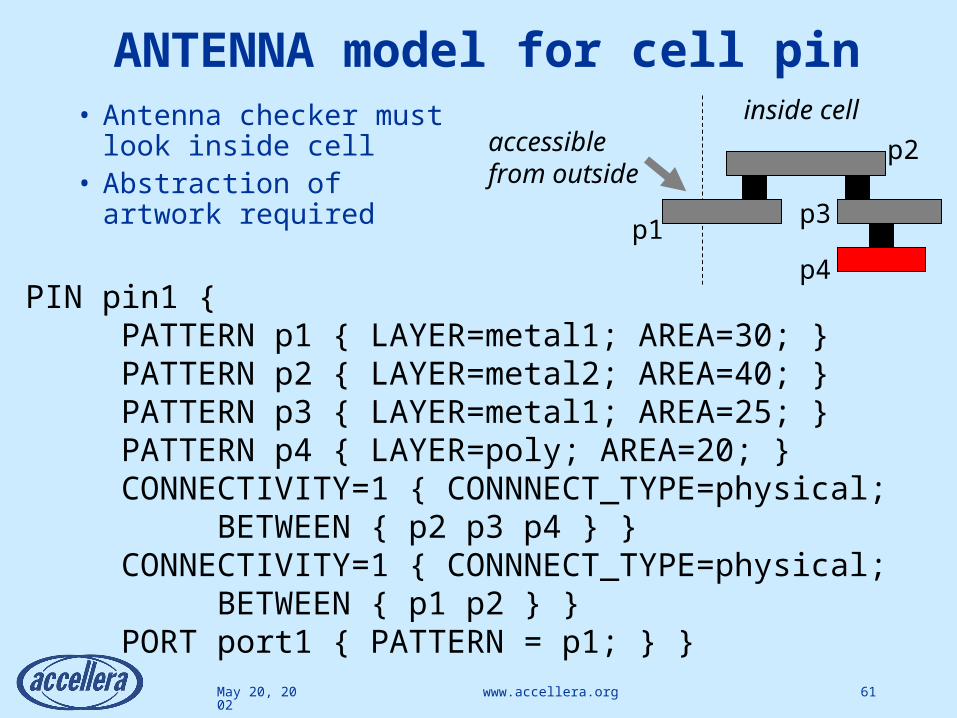
ANTENNA model for cell pin• Antenna checker must
look inside cell• Abstraction of artwork
required
PIN pin1 {PATTERN p1 { LAYER=metal1; AREA=30; }PATTERN p2 { LAYER=metal2; AREA=40; }PATTERN p3 { LAYER=metal1; AREA=25; }PATTERN p4 { LAYER=poly; AREA=20; }CONNECTIVITY=1 { CONNNECT_TYPE=physical;
BETWEEN { p2 p3 p4 } }CONNECTIVITY=1 { CONNNECT_TYPE=physical;
BETWEEN { p1 p2 } }PORT port1 { PATTERN = p1; } }
accessiblefrom outside
inside cell
p1
p2
p3
p4
May 20, 2002 www.accellera.org 62
ANTENNA summary
• ALF supports ANTENNA technology rules• Layer-specific and cumulative rules• Partially cumulative rules (air gap layer)• Diffusion layer involved in rule
• ALF supports hierarchical ANTENNA model• Abstract artwork model for cell pin• Sufficient detail for accurate antenna check• Does not reveal artwork geometry• Suitable for IP modeling
May 20, 2002 www.accellera.org 63
Conclusion and outlook• ALF provides comprehensive modeling support
• Timing with sign-off accuracy• Power from RTL to layout level• Signal integrity, reliability, manufacturability
• ALF is already deployed in the industry• Production-proven EDA tools• ASIC vendor libraries• Commercial library and IP providers
• ALF is a truly open standard• Vendor neutral• Forward looking• Recognized by IEEE and IEC

May 20, 2002 www.accellera.org 64
ALF resources available to the Industry
• ALF tutorial at CICC 2001• ALF paper at DATE 2002 Designers’ Forum• ALF specification documents
Available for download at
http://www.ascinc.com
Available for download at
http://www.eda.org/alf
• Free ALF parser from Alternative Systems Concepts
ascasc

May 20, 2002 www.accellera.org 65
ALF deployment in the industry
ascasc
I/F to Milkyway DB
Donation of free ALF parser
I/F to Volcano DB
Native lib for timing, power, SI tools
Native lib for RTL prototyping tool
Lib support from major ASIC vendors
Sponsoring organization

May 20, 2002 www.accellera.org 66
ALF covers superset of any other library combination
Timing macromodelPower macromodelSignal integrity macromodelAbstract physical modelInterconnect analysis modelCell timingCell powerCell signal integrityLayoutReliability Manufacturability
ALF
System
Silicon
OLA
OLA
.lef
.lef
STAMP
.lib