jeita eda -wg activity and study of interconnect model part-3 · jeita eda -wg activity and study...
TRANSCRIPT
1
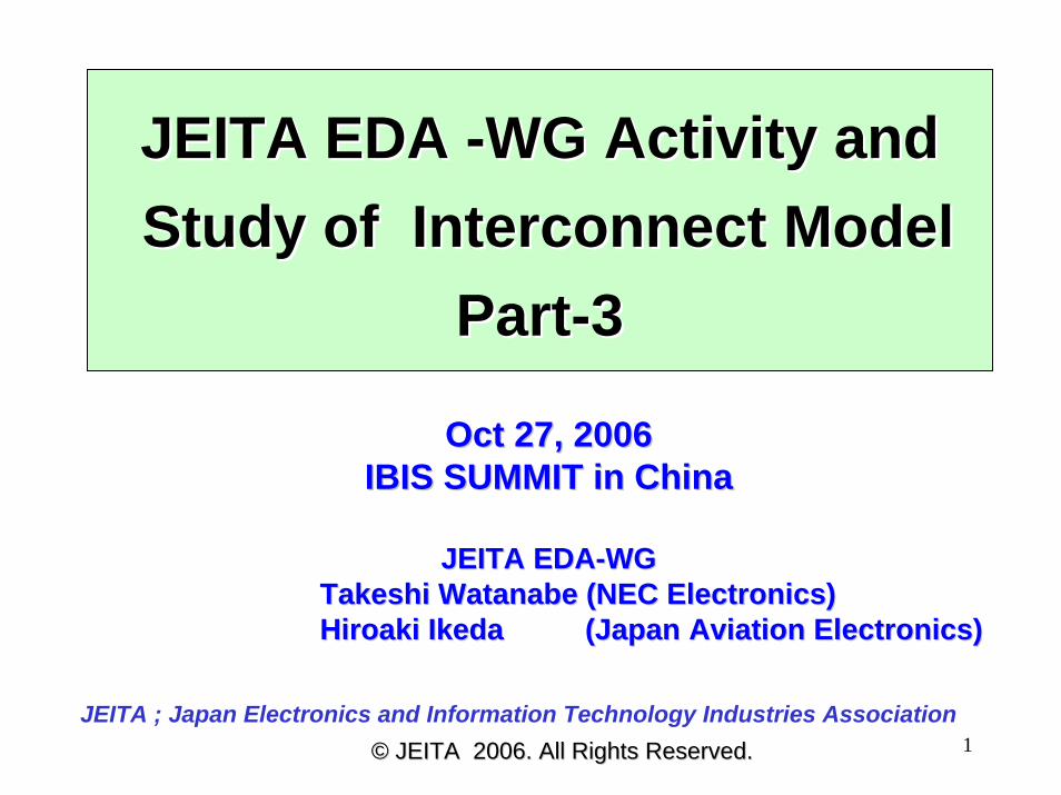
JEITA EDA JEITA EDA --WG Activity andWG Activity andStudy of Interconnect ModelStudy of Interconnect Model
PartPart--33
JEITA ; Japan Electronics and Information Technology Industries Association©© JEITA 2006. All Rights Reserved.JEITA 2006. All Rights Reserved.
Oct 27, 2006Oct 27, 2006IBIS SUMMIT in China IBIS SUMMIT in China
JEITA EDAJEITA EDA--WGWGTakeshi Watanabe (NEC Electronics) Takeshi Watanabe (NEC Electronics) Hiroaki Ikeda (Japan Hiroaki Ikeda (Japan Aviation ElectronicsAviation Electronics))

2
Outlines Outlines
1.1. JEITA EDAJEITA EDA--WG ActivitiesWG Activities
2. Short Term Direction of JEITA EDA WG2. Short Term Direction of JEITA EDA WG
3. Study of Interconnect Model 3. Study of Interconnect Model
4. Progress Report4. Progress Report
©© JEITA 2006. All Rights Reserved.JEITA 2006. All Rights Reserved.

3
EDA Model for
(Digital , RF, and Analog circuits)
Cellular Phone, LCD /PDP TV, Digital Camera/Video, DVD Recorder
Auto Mobile Electronics ?(Motor Drive, EMC)
Digital Consumer Electronics
< Applicability of IBIS V4.1 >
Objectives of JEITA EDAObjectives of JEITA EDA1. JEITA EDA1. JEITA EDA--WG ActivitiesWG Activities
©© JEITA 2006. All Rights Reserved.JEITA 2006. All Rights Reserved.

4
EMI, SI and PI for Digital Consumer Electronics
EMI, SI and PI for Digital Consumer Electronics
<Background>
EMI High-speed Clock Frequency
SI DDR, PCI, PCI-Express
PI High density and Large scale IC
SiP and Module, PCB level
EMI, SI and PI Simulation Technology©© JEITA 2006. All Rights Reserved.JEITA 2006. All Rights Reserved.
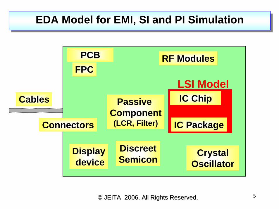
5
DiscreetSemicon
PCB
Passive Component(LCR, Filter)
RF Modules
Displaydevice
Connectors
Cables
FPC
Crystal Oscillator
IC Package
IC ChipLSI Model
EDA Model for EMI, SI and PI SimulationEDA Model for EMI, SI and PI Simulation
©© JEITA 2006. All Rights Reserved.JEITA 2006. All Rights Reserved.
6
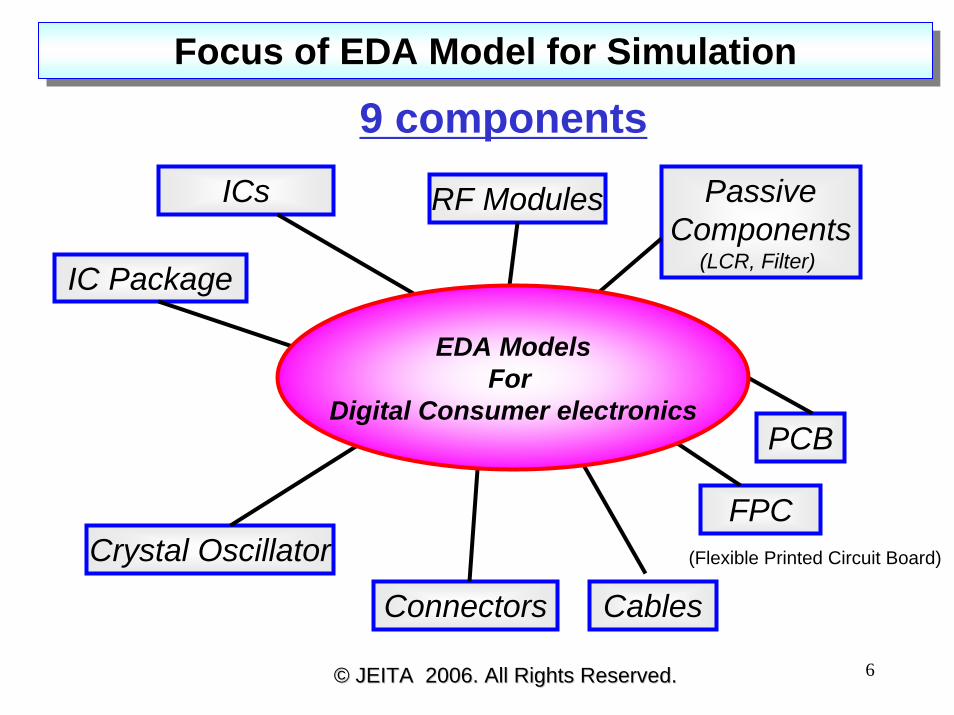
ICs
IC Package
PassiveComponents
(LCR, Filter)
Crystal Oscillator
Connectors Cables
PCB
FPC
RF Modules
EDA ModelsFor
Digital Consumer electronics
Focus of EDA Model for SimulationFocus of EDA Model for Simulation
9 components
(Flexible Printed Circuit Board)
©© JEITA 2006. All Rights Reserved.JEITA 2006. All Rights Reserved.

7
NECELToshiba TDK
Murata
CMKCybernet
EDA ModelsEDA ModelsFor For
Digital Consumer electronicsDigital Consumer electronics
DigitalConsumerElectronicsSupplier
EDA (internal/vendor)
Connectors
PCB
Semicon Passive Components
JAE
JEITA EDA-WG MemberJEITA EDA-WG Member16 Major Companies
FujitsuCadence Japan
OptimalCybernet System
PanasonicSonySharpCanon
ToshibaMitsubishi
©© JEITA 2006. All Rights Reserved.JEITA 2006. All Rights Reserved.
8©© JEITA 2006. All Rights Reserved.JEITA 2006. All Rights Reserved.
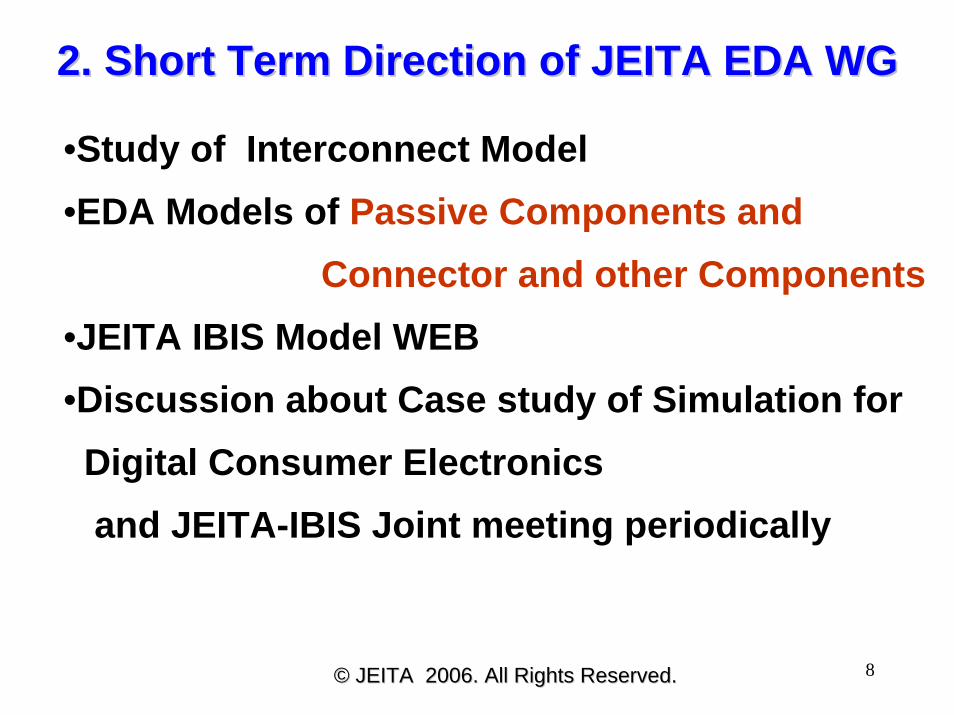
2. Short Term Direction of JEITA EDA WG2. Short Term Direction of JEITA EDA WG
•Study of Interconnect Model •EDA Models of Passive Components and
Connector and other Components•JEITA IBIS Model WEB•Discussion about Case study of Simulation for Digital Consumer Electronics and JEITA-IBIS Joint meeting periodically
9©© JEITA 2006. All Rights Reserved.JEITA 2006. All Rights Reserved.
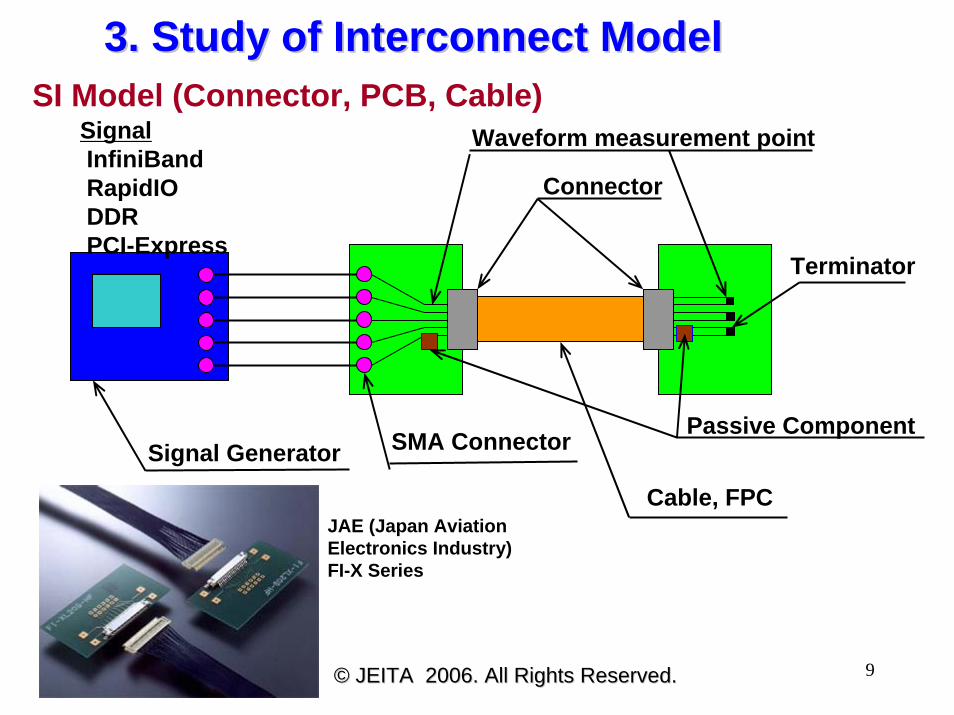
3. Study of Interconnect Model 3. Study of Interconnect Model SI Model (Connector, PCB, Cable)
Cable, FPC
Connector
SMA ConnectorSignal Generator
Waveform measurement point
Terminator
SignalInfiniBandRapidIODDRPCI-Express
JAE (Japan Aviation Electronics Industry)FI-X Series
Passive Component
10©© JEITA 2006. All Rights Reserved.JEITA 2006. All Rights Reserved.
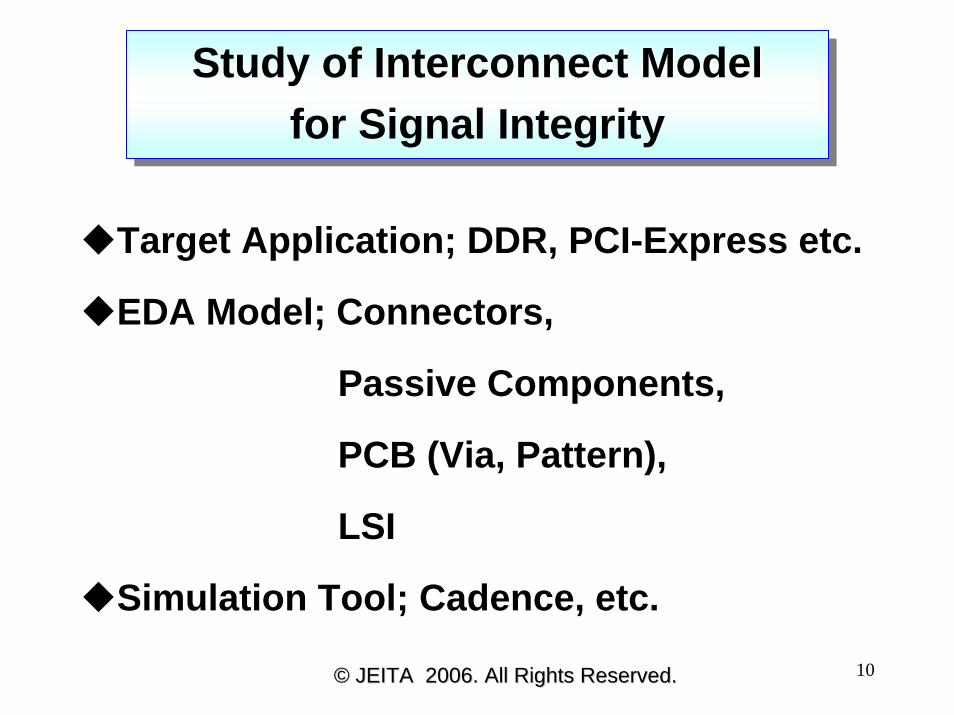
Target Application; DDR, PCI-Express etc.
EDA Model; Connectors,
Passive Components,
PCB (Via, Pattern),
LSI
Simulation Tool; Cadence, etc.
Study of Interconnect Modelfor Signal Integrity
Study of Interconnect ModelInterconnect Modelfor Signal Integrity
11
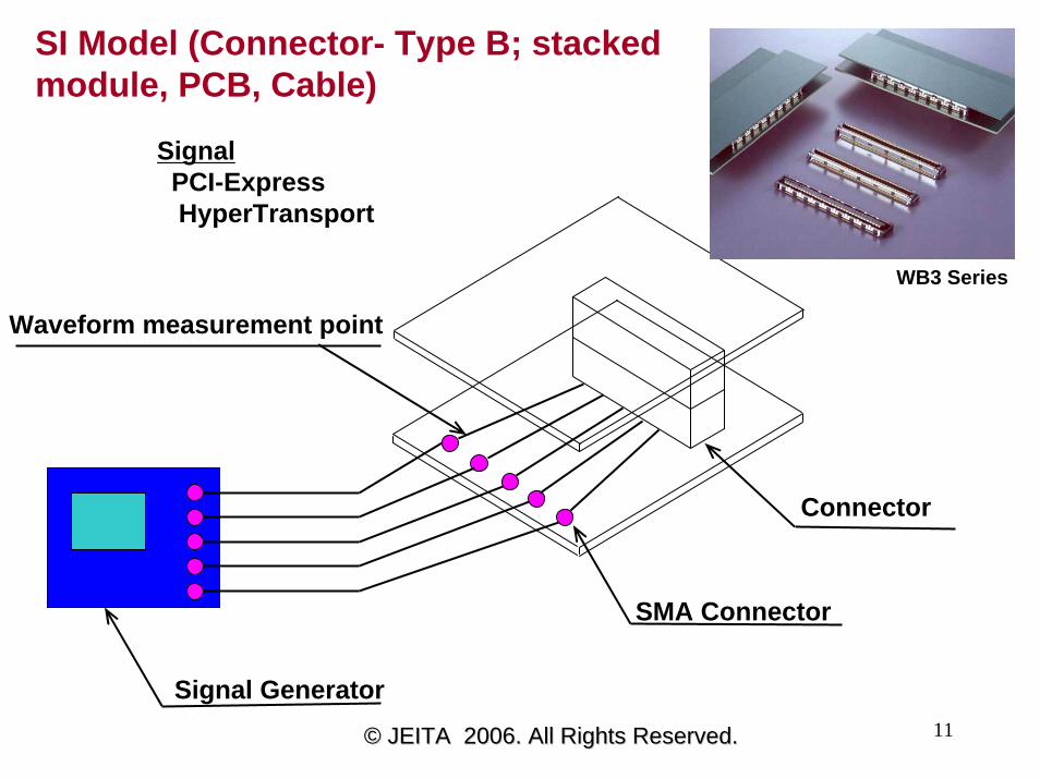
Waveform measurement point
SignalPCI-ExpressHyperTransport
WB3 Series
©© JEITA 2006. All Rights Reserved.JEITA 2006. All Rights Reserved.
Connector
Signal Generator
SMA Connector
SI Model (Connector- Type B; stacked module, PCB, Cable)

12
SignalPCI-ExpressHyperTransport
MJ04 Series
Waveform measurement point
Connector
Signal GeneratorSMA Connector
©© JEITA 2006. All Rights Reserved.JEITA 2006. All Rights Reserved.
SI Model (Connector- Type C, PCB, Cable)

13©© JEITA 2006. All Rights Reserved.JEITA 2006. All Rights Reserved.
Measurement
Simulation
TML
Equivalent circuit
Simulation ModelSimulation Model

14©© JEITA 2006. All Rights Reserved.JEITA 2006. All Rights Reserved.
Evaluation BoardEvaluation Board
SMAR006D00SMA Connector
SMA Connector
Fi-X Connector
spacer
Connector
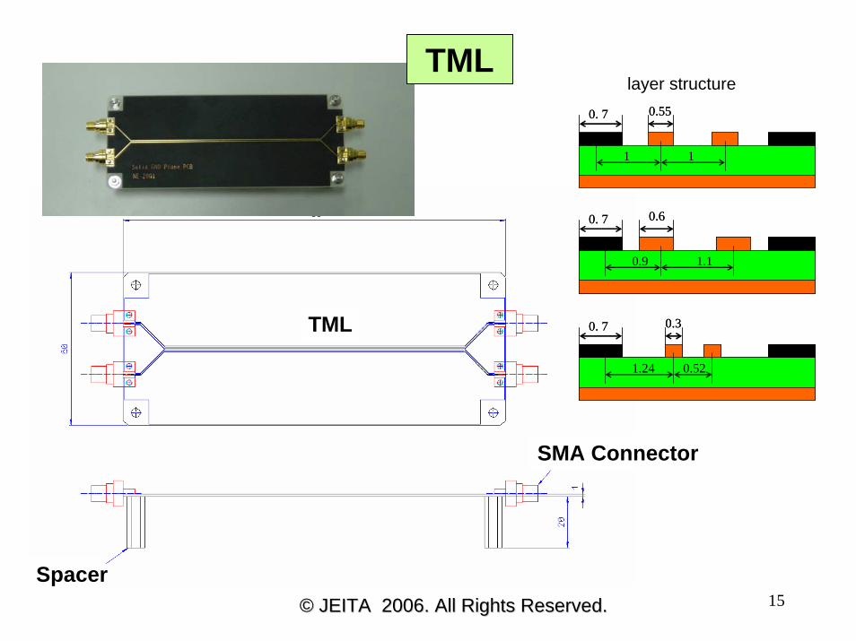
15
SMA Connector
layer structure 0.550. 7
1 1
0.550. 7
1 1
0.9 1.1
0.60. 7
0.9 1.1
0.60. 7
0.30. 7
1.24 0.52
0.30. 7
1.24 0.52
©© JEITA 2006. All Rights Reserved.JEITA 2006. All Rights Reserved.Spacer
TML
TML

16©© JEITA 2006. All Rights Reserved.JEITA 2006. All Rights Reserved.
Passive Components
Passive Components SMA Connector
Spacer
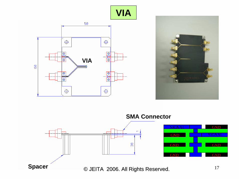
17
SIGNAL
GND
GND
GND
SIGNAL
GND
GND
GND
SMA Connector
Spacer ©© JEITA 2006. All Rights Reserved.JEITA 2006. All Rights Reserved.
VIA
VIA
18
•Study of Interconnect Model
©© JEITA 2006. All Rights Reserved.JEITA 2006. All Rights Reserved.
~ October of 2006
4. JEITA EDA4. JEITA EDA--WGWGProgress ReportProgress Report

19
Ω/H/S/F
Spice RLGCS-para
Model
Measurement
Compare Measurement with Simulation
©© JEITA 2006. All Rights Reserved.JEITA 2006. All Rights Reserved.
Simulation
MHz~GHz

20
Contents
0. Measurement and Simulation Environment0.1 Measurement equipment and simulation tools
1. Detail of Measurement and simulation1.1 Measurement1.2 Simulation
2. Comparison between Measurement and Simulation2.1 Eye-Diagram and Discrete Waveform
3. Simulation with Measured EDA models3.1 Eye-Diagram
4. Accuracy of EDA models 4.1 TDR waveform for PCB trace4.2 S-parameters of device models (Filters,Via,Connector,Cable)
5. Conclusion
Study of Interconnect Model
©© JEITA 2006. All Rights Reserved.JEITA 2006. All Rights Reserved.
21
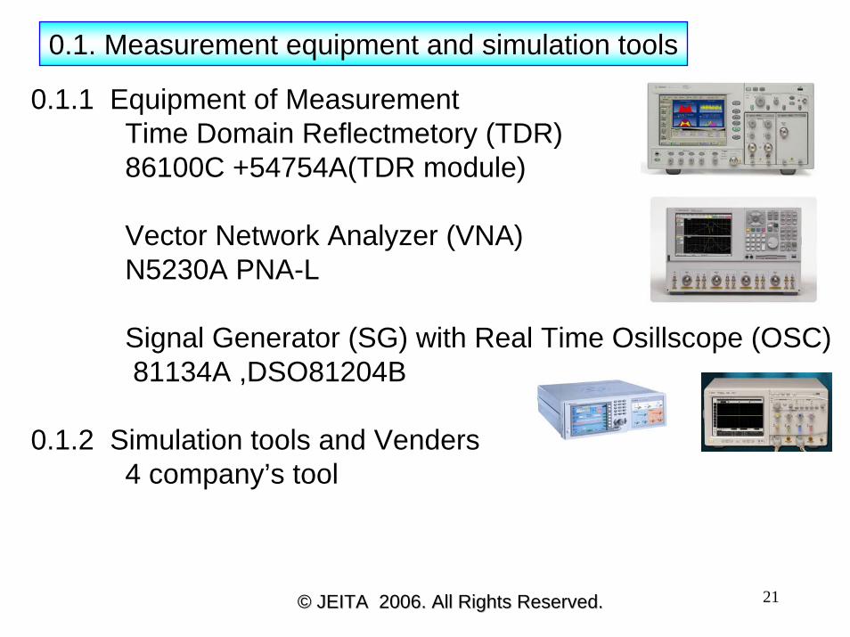
0.1.1 Equipment of MeasurementTime Domain Reflectmetory (TDR)86100C +54754A(TDR module)
Vector Network Analyzer (VNA)N5230A PNA-L
Signal Generator (SG) with Real Time Osillscope (OSC)81134A ,DSO81204B
0.1.2 Simulation tools and Venders4 company’s tool
0.1. Measurement equipment and simulation tools
©© JEITA 2006. All Rights Reserved.JEITA 2006. All Rights Reserved.
22
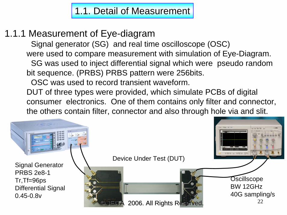
1.1.1 Measurement of Eye-diagramSignal generator (SG) and real time oscilloscope (OSC)
were used to compare measurement with simulation of Eye-Diagram. SG was used to inject differential signal which were pseudo random
bit sequence. (PRBS) PRBS pattern were 256bits.OSC was used to record transient waveform.
DUT of three types were provided, which simulate PCBs of digital consumer electronics. One of them contains only filter and connector, the others contain filter, connector and also through hole via and slit.
Signal GeneratorPRBS 2e8-1Tr,Tf=96psDifferential Signal0.45-0.8v
OscillscopeBW 12GHz40G sampling/s
Device Under Test (DUT)
1.1. Detail of Measurement
©© JEITA 2006. All Rights Reserved.JEITA 2006. All Rights Reserved.

23
1.1.2 Measurement of TDRTo verify characteristic Impedance of PCB, TDR was used.
The TDR injected differential step pulse and measured reflectionwaveform, then characteristic Impedance was calculated by the reflection waveform.
One side of DUT were left open in order to measure DUT of electric length which is propagation time to the end ports.
DUTTDR OSCTDR moduleBW 18GHzTr 35psec
1.1. Detail of Measurement
Open EndNot Terminated
©© JEITA 2006. All Rights Reserved.JEITA 2006. All Rights Reserved.

24
1.1.3 Measurement of S-parametersTo verify simulation models ,VNA were used to measure
S-parameters. The VNA has 4 ports, therefore it measures mixedmode S-parameters which are important parameter to investigate differential transmission line.
DUT
1.1. Detail of Measurement
4 ports VNABW 10M-20GHzIFBW 100kMeasured points 2000Averaging 10 times
©© JEITA 2006. All Rights Reserved.JEITA 2006. All Rights Reserved.

25
1. EDA models were provided by component manufacturer.
2. PCB models were extracted from CAD data by simulation tools.PCB manufacturer does not provide EDA model.They provide only layer structure, wire width, space between wires and dielectric constant.
3. EDA models were S-parameters or Equivalent Circuits.
1.2. Detail of simulationEDA models
©© JEITA 2006. All Rights Reserved.JEITA 2006. All Rights Reserved.

26
1. Eye-DiagramOnly EDA model provided by the manufacturer.To verify Whether the measurement agrees with the simulation Measured S-parametersTo verify whether each simulator accept S-parameters.
2. TDR WaveformOnly wire of PCBTo verify whether EDA model of PCB which is extracted by each simulatoris correct.
3. S-parametersEach EDA models To verify accuracy of each EDA models
1.2. Detail of simulationSimulation Items
©© JEITA 2006. All Rights Reserved.JEITA 2006. All Rights Reserved.

27
SMA (S-par)
Source 50ohmsTRL model
Filter (equivalentCircuit)
50 ohmsMeasurement points
Cable and Connector(S-par)
SGSource points
Via (S-par)
Measurement points
OSC
1.2. Detail of simulation#68 DUT and Simulation model
©© JEITA 2006. All Rights Reserved.JEITA 2006. All Rights Reserved.
210mm100mm 100mm
Cross section
0.35 0.65 0.35
0.2
0.05
0.035
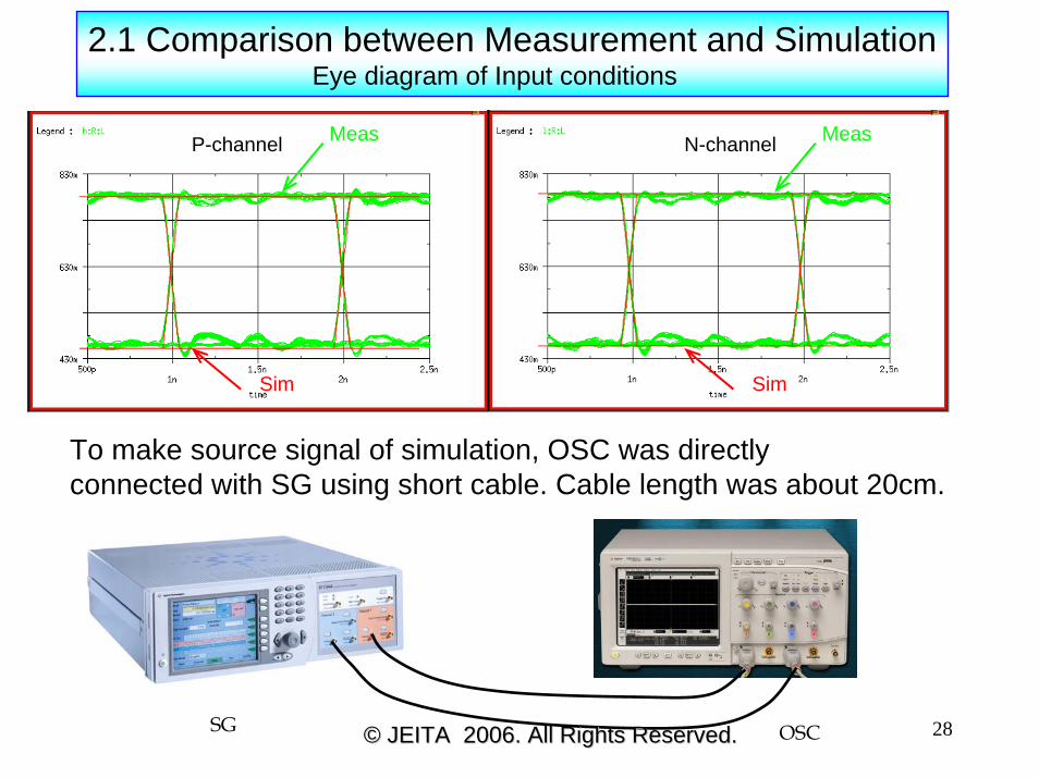
28
Meas
Sim
P-channel Meas
Sim
N-channel
SG OSC
To make source signal of simulation, OSC was directly connected with SG using short cable. Cable length was about 20cm.
2.1 Comparison between Measurement and SimulationEye diagram of Input conditions
©© JEITA 2006. All Rights Reserved.JEITA 2006. All Rights Reserved.
29
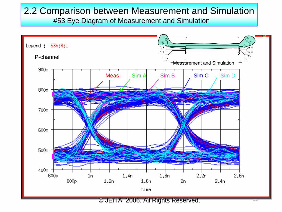
P-channel
Sim AMeas Sim CSim B
Measurement and Simulation
2.2 Comparison between Measurement and Simulation#53 Eye Diagram of Measurement and Simulation
Sim D
©© JEITA 2006. All Rights Reserved.JEITA 2006. All Rights Reserved.

30
N-channel
Sim AMeas Sim CSim B
2.3 Comparison between Measurement and Simulation#53 Eye Diagram of Measurement and Simulation
Sim D
©© JEITA 2006. All Rights Reserved.JEITA 2006. All Rights Reserved.
Measurement and Simulation

31
Meas
2.4 Comparison between Measurement and Simulation#53 Discrete Waveform of Measurement and Simulation
Sim ASim B
Sim C
Sim D
P-channel
©© JEITA 2006. All Rights Reserved.JEITA 2006. All Rights Reserved.
32
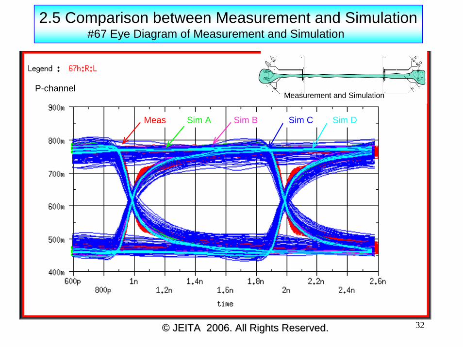
Sim AMeas Sim CSim B
2.5 Comparison between Measurement and Simulation#67 Eye Diagram of Measurement and Simulation
P-channelMeasurement and Simulation
Sim D
©© JEITA 2006. All Rights Reserved.JEITA 2006. All Rights Reserved.

33
MeasP-channel
2.6 Comparison between Measurement and Simulation#67 Discrete Waveform of Measurement and Simulation
Sim BSim A
Sim C
Sim D
©© JEITA 2006. All Rights Reserved.JEITA 2006. All Rights Reserved.

34
Sim AMeas Sim CSim B
2.7 Comparison between Measurement and Simulation#68 Eye Diagram of Measurement and Simulation
P-channelMeasurement and Simulation
Sim D
©© JEITA 2006. All Rights Reserved.JEITA 2006. All Rights Reserved.
35
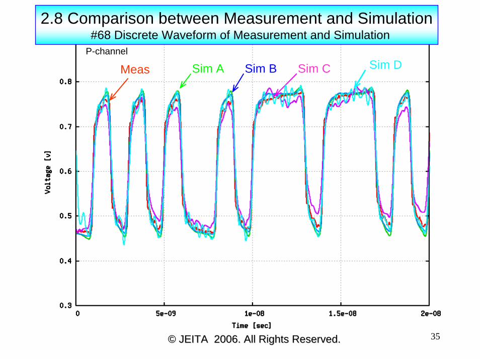
MeasP-channel
Sim A Sim B Sim C Sim D
2.8 Comparison between Measurement and Simulation#68 Discrete Waveform of Measurement and Simulation
©© JEITA 2006. All Rights Reserved.JEITA 2006. All Rights Reserved.
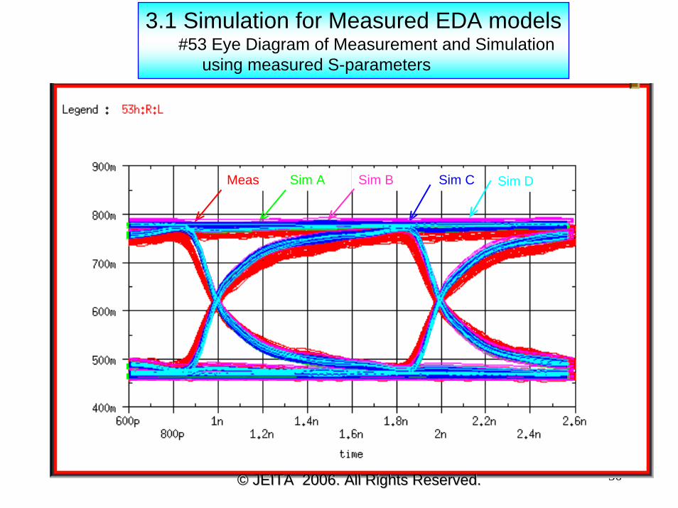
36#32
Sim AMeas Sim CSim B
3.1 Simulation for Measured EDA models#53 Eye Diagram of Measurement and Simulation
using measured S-parameters
Sim D
©© JEITA 2006. All Rights Reserved.JEITA 2006. All Rights Reserved.

37
Sim AMeas Sim CSim B
3.2 Simulations for Measured EDA models#67 Eye Diagram of Measurement and Simulation
using measured S-parameters
Sim D
©© JEITA 2006. All Rights Reserved.JEITA 2006. All Rights Reserved.
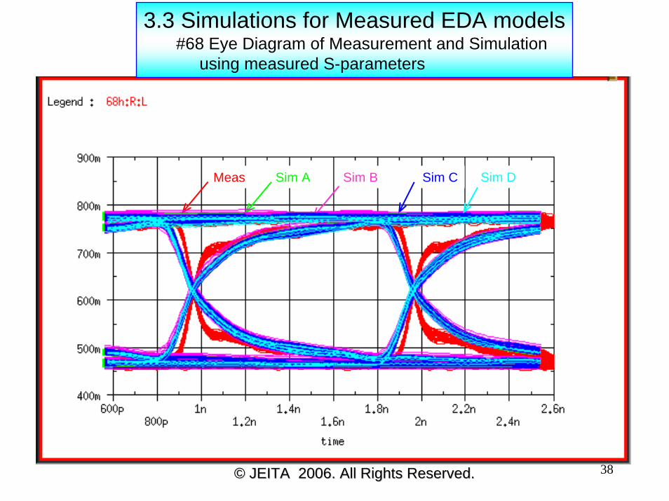
38
Sim AMeas Sim CSim B
3.3 Simulations for Measured EDA models#68 Eye Diagram of Measurement and Simulation
using measured S-parameters
Sim D
©© JEITA 2006. All Rights Reserved.JEITA 2006. All Rights Reserved.

39
0.33
0.36
53.5u235uZdiff=104ohrm
0.35
0.38
53.5u235uZdiff=101ohrm
Meas
Sim (Different x-sections) Sim (Same x-section)
4. Accuracy of EDA models 4.1 Measured and Simulated TDR waveform
©© JEITA 2006. All Rights Reserved.JEITA 2006. All Rights Reserved.
40
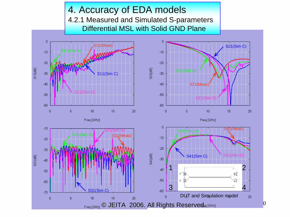
S11(Meas)
S11(Sim C)
S11(Sim A)
S21(Meas)
S21(Sim C)
S21(Sim A)
S31(Meas)S31(Sim A)
4. Accuracy of EDA models 4.2.1 Measured and Simulated S-parameters
Differential MSL with Solid GND Plane
S31(Sim D)
S21(Sim D)
S31(Sim C)
1
3
2
4DUT and Simulation model
S41(Sim C)
S41(Meas)S41(Sim A)
S41(Sim D)
S11(Sim D)
©© JEITA 2006. All Rights Reserved.JEITA 2006. All Rights Reserved.

41
MeasEquiv(Sim)
S-par(Sim) Meas
Equiv(Sim)
S-par(Sim)
Meas
Equiv(Sim)
S-par(Sim)
Equiv(Sim)
MeasS-par(Sim)
1
3
2
4
4. Accuracy of EDA models4.2.2 Measured and Simulated S-parameters
Filter A
©© JEITA 2006. All Rights Reserved.JEITA 2006. All Rights Reserved.
42
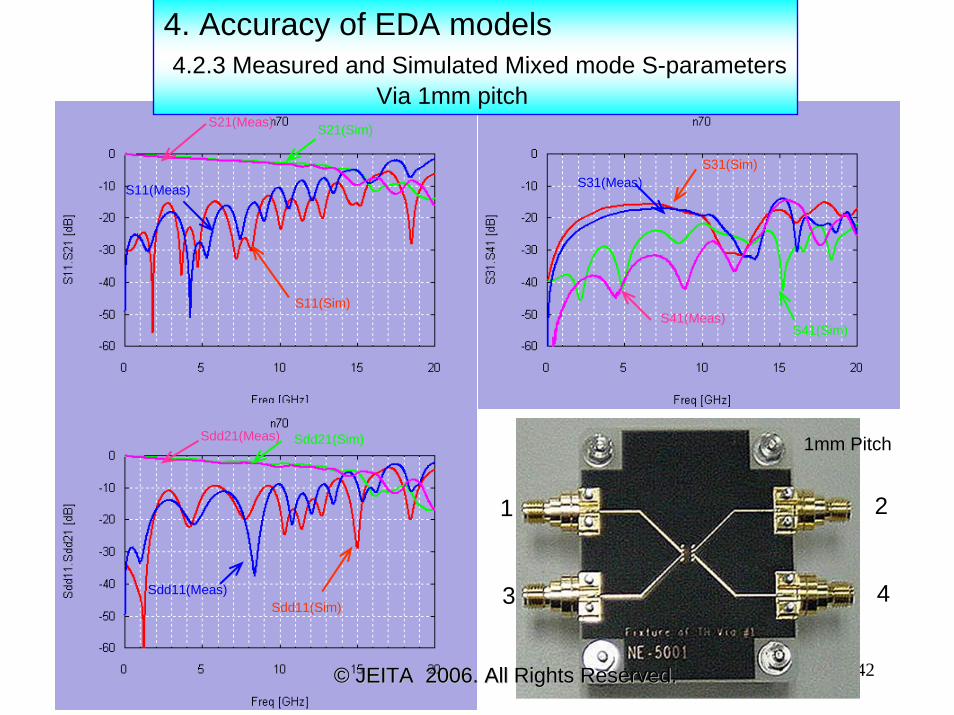
S21(Meas)
S11(Sim)
S11(Meas)
S21(Sim)
S41(Meas)
S31(Sim)S31(Meas)
S41(Sim)
Sdd21(Meas)
Sdd11(Sim)Sdd11(Meas)
Sdd21(Sim) 1mm Pitch
1
3
2
4
4. Accuracy of EDA models4.2.3 Measured and Simulated Mixed mode S-parameters
Via 1mm pitch
©© JEITA 2006. All Rights Reserved.JEITA 2006. All Rights Reserved.

43DUT and Simulation model
S41(Meas)
S31(Sim)
S31(Meas)
S41(Sim)
S11(Meas)S11(Sim)
S21(Meas)S21(Sim)
Sdd21(Meas)
Sdd11(Meas)
Sdd21(Sim)
Sdd11(Sim)
Port 1Port 3
Port 2Port 4
4. Accuracy of EDA models4.2.4 Edge of Connector Cable
©© JEITA 2006. All Rights Reserved.JEITA 2006. All Rights Reserved.

44
5. Conclusion
1. Measurement and simulation of Interconnect model were done.
2. Simulation used by EDA models whom componentmanufacturer provides and measurement are nearly agreed.
3.Each simulator accepts S-parameters and directly simulate them.
4.It is necessary to note that a design value and an actual value might be different when EDA model of PCB is made.
©© JEITA 2006. All Rights Reserved.JEITA 2006. All Rights Reserved.
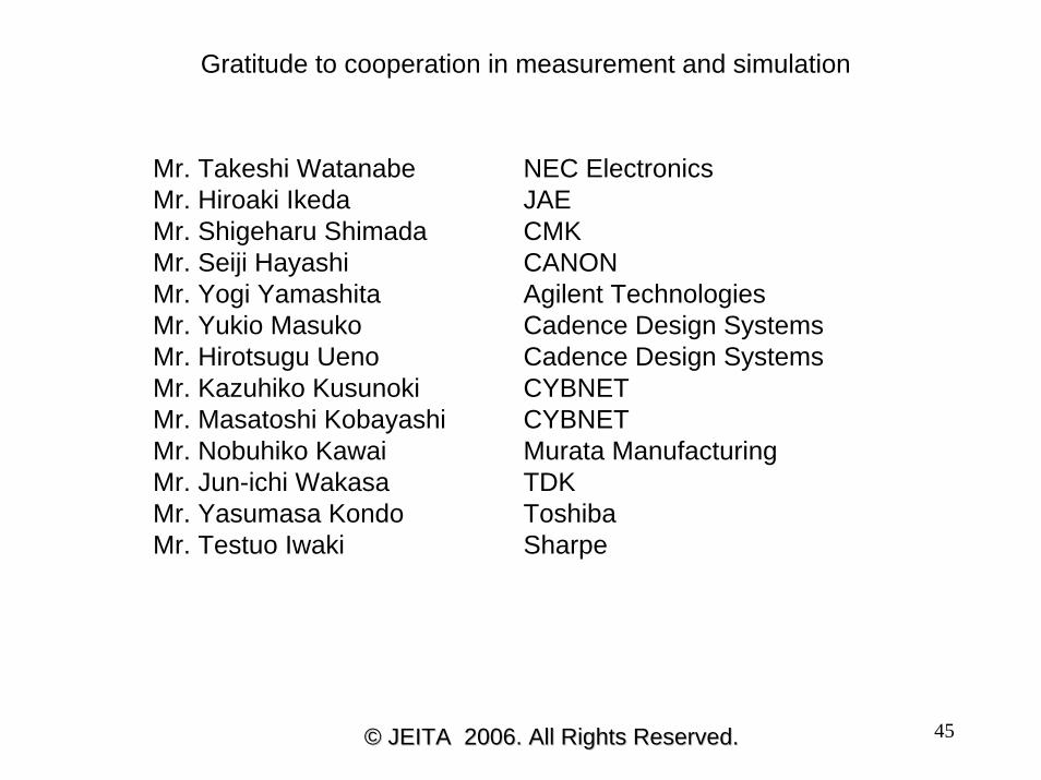
45
Mr. Takeshi WatanabeMr. Hiroaki Ikeda Mr. Shigeharu Shimada Mr. Seiji Hayashi Mr. Yogi Yamashita Mr. Yukio Masuko Mr. Hirotsugu Ueno Mr. Kazuhiko Kusunoki Mr. Masatoshi Kobayashi Mr. Nobuhiko Kawai Mr. Jun-ichi WakasaMr. Yasumasa Kondo Mr. Testuo Iwaki
Gratitude to cooperation in measurement and simulation
NEC ElectronicsJAECMKCANONAgilent Technologies Cadence Design Systems Cadence Design Systems CYBNETCYBNETMurata ManufacturingTDK ToshibaSharpe
©© JEITA 2006. All Rights Reserved.JEITA 2006. All Rights Reserved.
46
We hope to discuss case study of IBIS with you
periodically
Thank you for all the helpEIA/IBIS Committee!
©© JEITA 2006. All Rights Reserved.JEITA 2006. All Rights Reserved.
再見