isl8488e, isl8489e, isl8490e, isl8491e datasheet and tx output pins) applications, so they are ideal...
TRANSCRIPT

FN6073Rev.4.00
July 26, 2007
ISL8488E, ISL8489E, ISL8490E, ISL8491E±15kV ESD Protected, 5V, Low Power, High Speed and Slew Rate Limited, Full Duplex, RS-485/RS-422 Transceivers
DATASHEET
The ISL8488E, ISL8489E, ISL8490E, ISL8491E devices are ESD protected, BiCMOS, 5V powered, single transceivers that meet both the RS-485 and RS-422 standards for balanced communication. Each driver output and receiver input is protected against ±15kV ESD strikes, without latch-up. Unlike competitive versions, these Intersil devices are specified for 10% tolerance supplies (4.5V to 5.5V).
These devices are configured for full duplex (separate Rx input and Tx output pins) applications, so they are ideal for RS-422 networks requiring high ESD tolerance on the bus pins. The ISL8488E, ISL8490E are 8 Ld versions without Rx and Tx output enables. The other two versions include Rx and Tx output enable pins in a standard 14 Ld pinout.
The ISL8488E, ISL8489E utilize slew rate limited drivers which reduce EMI, and minimize reflections from improperly terminated transmission lines, or unterminated stubs in multidrop and multipoint applications.
Data rates up to 10Mbps are achievable by using the ISL8490E, ISL8491E, which feature higher slew rates.
The devices present a “single unit load” to the RS-485 bus, which allows a total of 32 transmitters and receivers on the network. For “1/8 unit load” versions (256 devices on the bus), please refer to the ISL4489E, ISL4491E data sheet.
Receiver (Rx) inputs feature a “fail-safe if open” design, which ensures a logic high Rx output if Rx inputs are floating.
Driver (Tx) outputs are short circuit protected, even for voltages exceeding the power supply voltage. Additionally, on-chip thermal shutdown circuitry disables the Tx outputs to prevent damage if power dissipation becomes excessive.
Features
• RS-485 I/O Pin ESD Protection 15kV HBM
- Class 3 ESD Level on all Other Pins . . . . . . >7kV HBM
• High Data Rates (ISL8490E, ISL8491E) . . up to 10Mbps
• Slew Rate Limited for Error Free Data Transmission (ISL8488E, ISL8489E)
• Single Unit Load Allows up to 32 Devices on the Bus(See ISL4489E, ISL4491E for 256 Devices on Bus)
• Low Quiescent Current:
- 120µA (ISL8488E)
- 140µA (ISL8489E)
- 370µA (ISL8490E, ISL8491E)
• -7V to +12V Common Mode Input Voltage Range
• Three-State Rx and Tx Outputs (Except ISL8488E, ISL8490E)
• Full Duplex Pinout
• Operates from a Single +5V Supply (10% Tolerance)
• Current Limiting and Thermal Shutdown for Driver Overload Protection
• Pb-Free Plus Anneal Available (RoHS Compliant)
Applications
• Factory Automation
• Security Networks
• Building Environmental Control Systems
• Industrial/Process Control Networks
• Level Translators (e.g., RS-232 to RS-422)
• RS-232 “Extension Cords”
TABLE 1. SUMMARY OF FEATURES
PART NUMBER
HALF/FULL DUPLEX HIGH ESD?
NO. OF DEVICES ALLOWED ON BUS
DATA RATE (Mbps)
SLEW-RATE LIMITED?
RECEIVER/DRIVER ENABLE?
QUIESCENT ICC (A)
PIN COUNT
ISL8488E Full Yes 32 0.25 Yes No 120 8
ISL8489E Full Yes 32 0.25 Yes Yes 140 14
ISL8490E Full Yes 32 10 No No 370 8
ISL8491E Full Yes 32 10 No Yes 370 14
FN6073 Rev.4.00 Page 1 of 13July 26, 2007
ISL8488E, ISL8489E, ISL8490E, ISL8491E
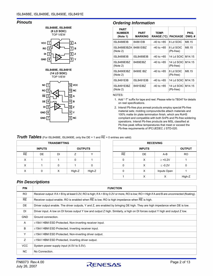
PinoutsISL8488E, ISL8490E
(8 LD SOIC)TOP VIEW
ISL8489E, ISL8491E(14 LD SOIC)
TOP VIEW
Truth Tables (For ISL8488E, ISL8490E, only the DE = 1 and RE = 0 entries are valid)
VCC
RO
DI
GND
1
2
3
4
8
7
6
5
A
B
Z
YD
R
NC
RO
RE
DE
DI
GND
GND
VCC
NC
A
B
Z
Y
NC
1
2
3
4
5
6
7
14
13
12
11
10
9
8
D
R
Ordering Information
PART NUMBER(Note 1)
PARTMARKING
TEMP.RANGE (°C) PACKAGE
PKG.DWG. #
ISL8488EIB 8488 EIB -40 to +85 8 Ld SOIC M8.15
ISL8488EIBZA(Note 2)
8488 EIBZ -40 to +85 8 Ld SOIC(Pb-free)
M8.15
ISL8489EIB ISL8489EIB -40 to +85 14 Ld SOIC M14.15
ISL8489EIBZ(Note 2)
8489EIBZ -40 to +85 14 Ld SOIC(Pb-free)
M14.15
ISL8490EIBZ(Note 2)
8490E IBZ -40 to +85 8 Ld SOIC(Pb-free)
M8.15
ISL8491EIB ISL8491EIB -40 to +85 14 Ld SOIC M14.15
ISL8491EIBZ(Note 2)
8491EIBZ -40 to +85 14 Ld SOIC(Pb-free)
M14.15
NOTES:
1. Add “-T” suffix for tape and reel. Please refer to TB347 for details on reel specifications.
2. Intersil Pb-free plus anneal products employ special Pb-free material sets; molding compounds/die attach materials and 100% matte tin plate termination finish, which are RoHS compliant and compatible with both SnPb and Pb-free soldering operations. Intersil Pb-free products are MSL classified at Pb-free peak reflow temperatures that meet or exceed the Pb-free requirements of IPC/JEDEC J STD-020.
TRANSMITTING
INPUTS OUTPUTS
RE DE DI Z Y
X 1 1 0 1
X 1 0 1 0
X 0 X High-Z High-Z
RECEIVING
INPUTS OUTPUT
RE DE A-B RO
0 X +0.2V 1
0 X -0.2V 0
0 X Inputs Open 1
1 X X High-Z
Pin Descriptions
PIN FUNCTION
RO Receiver output: If A > B by at least 0.2V, RO is high; If A < B by 0.2V or more, RO is low; RO = High if A and B are unconnected (floating).
RE Receiver output enable. RO is enabled when RE is low; RO is high impedance when RE is high.
DE Driver output enable. The driver outputs, Y and Z, are enabled by bringing DE high. They are high impedance when DE is low.
DI Driver input. A low on DI forces output Y low and output Z high. Similarly, a high on DI forces output Y high and output Z low.
GND Ground connection.
A 15kV HBM ESD Protected, Non-inverting receiver input.
B 15kV HBM ESD Protected, Inverting receiver input.
Y 15kV HBM ESD Protected, Non-inverting driver output.
Z 15kV HBM ESD Protected, Inverting driver output.
VCC System power supply input (4.5V to 5.5V).
NC No Connection.
FN6073 Rev.4.00 Page 2 of 13July 26, 2007

ISL8488E, ISL8489E, ISL8490E, ISL8491E
Typical Operating Circuit
ISL8488E, ISL8490E
ISL8489E, ISL8491E
0.1µF+
D
R
8
7
6
5
1
2
3
4
VCC
GND
RO
DI
A
B
Y
Z
+5V
0.1µF+
D
R8
7
6
5
1
2
3
4
VCC
GND
RO
DI
A
B
Y
Z
+5V
RT
RT
0.1µF+
D
R
12
11
10
9
14
2
3
4
5
6, 7
VCC
GND
RO
RE
DE
DI
A
B
Y
Z
+5V
0.1µF+
D
R12
11
10
9
14
2
3
4
5
6, 7
VCC
GND
RO
RE
DE
DI
A
B
Y
Z
+5V
RT
RT
FN6073 Rev.4.00 Page 3 of 13July 26, 2007

ISL8488E, ISL8489E, ISL8490E, ISL8491E
Absolute Maximum Ratings Thermal Information
VCC to GND. . . . . . . . . . . . . . . . . . . . . . . . . . . . . . . . . . . . . . . . . 7VInput Voltages
DI, DE, RE . . . . . . . . . . . . . . . . . . . . . . . . . -0.5V to (VCC + 0.5V)Input/Output Voltages
A, B, Y, Z . . . . . . . . . . . . . . . . . . . . . . . . . . . . . . . . -8V to + 12.5VRO . . . . . . . . . . . . . . . . . . . . . . . . . . . . . . . -0.5V to (VCC + 0.5V)
Short Circuit DurationY, Z . . . . . . . . . . . . . . . . . . . . . . . . . . . . . . . . . . . . . . . Continuous
ESD Rating . . . . . . . . . . . . . . . . . . . . . . . . . See Specification Table
Thermal Resistance (Typical) JA (°C/W)
8 Ld SOIC Package (Note 3) . . . . . . . . . . . . . . . . . . 17014 Ld SOIC Package (Note 3) . . . . . . . . . . . . . . . . . 128
Maximum Junction Temperature (Plastic Package) . . . . . . +150°CMaximum Storage Temperature Range . . . . . . . . . . -65°C to +150°CPb-free reflow profile . . . . . . . . . . . . . . . . . . . . . . . . . .see link below
http://www.intersil.com/pbfree/Pb-FreeReflow.asp
Operating ConditionsTemperature Range. . . . . . . . . . . . . . . . . . . . . . . . . . -40°C to +85°C
CAUTION: Do not operate at or near the maximum ratings listed for extended periods of time. Exposure to such conditions may adversely impact product reliability andresult in failures not covered by warranty.
NOTE:
3. JA is measured with the component mounted on a low effective thermal conductivity test board in free air. See Tech Brief TB379 for details.
Electrical Specifications Test Conditions: VCC = 4.5V to 5.5V; Unless Otherwise Specified. Typicals are at VCC = 5V, TA = +25°C,(Note 4).
PARAMETER SYMBOL TEST CONDITIONSTEMP(°C)
MIN(NOTE 9) TYP
MAX(NOTE 9) UNITS
DC CHARACTERISTICS
Driver Differential VOUT (no load) VOD1 Full - - VCC V
Driver Differential VOUT (with load) VOD2 R = 50 (RS-422) (Figure 1) Full 2 3 - V
R = 27 (RS-485) (Figure 1) Full 1.5 2.3 5 V
Change in Magnitude of Driver Differential VOUT for Complementary Output States
VOD R = 27 or 50 (Figure 1) Full - 0.01 0.2 V
Driver Common-Mode VOUT VOC R = 27 or 50 (Figure 1) Full - - 3 V
Change in Magnitude of Driver Common-Mode VOUT for Complementary Output States
VOC R = 27 or 50 (Figure 1) Full - 0.01 0.2 V
Logic Input High Voltage VIH DE, DI, RE Full 2 - - V
Logic Input Low Voltage VIL DE, DI, RE Full 0.8 - - V
Logic Input Current IIN1 DI Full -2 - 2 A
DE, RE (Note 8) Full -40 - 40 A
Input Current (A, B) (Note 7) IIN2 DE = 0V, VCC = 0V or 4.5V to 5.5V
VIN = 12V Full - - 1 mA
VIN = -7V Full -0.8 - - mA
Driver Three-State Output Current (Y, Z) IOZD DE = 0V, -7V VO 12V (Note 8) Full -100 - 100 A
Receiver Differential Threshold Voltage VTH -7V VCM 12V Full -0.2 - 0.2 V
Receiver Input Hysteresis VTH VCM = 0V 25 - 70 - mV
Receiver Output High Voltage VOH IO = -4mA, VID = 200mV Full 3.5 - - V
Receiver Output Low Voltage VOL IO = 4mA, VID = 200mV Full - - 0.4 V
Receiver Three-State Output Current IOZR RE = VCC, 0.4V VO 2.4V (Note 8) Full - - 1 A
Receiver Input Resistance RIN -7V VCM 12V Full 12 - - k
No-Load Supply Current (Note 5) ICC ISL8488E, DI = 0V or VCC Full - 120 140 A
ISL8489E, DE, DI, RE = 0V or VCC Full - 140 190 A
ISL8490E/ISL8491E, DE, DI, RE = 0V or VCC
Full - 370 460 A
Driver Short-Circuit Current, VO = High or Low
IOSD1 DE = VCC, -7V VY or VZ 12V (Note 6) Full 35 - 250 mA
FN6073 Rev.4.00 Page 4 of 13July 26, 2007

ISL8488E, ISL8489E, ISL8490E, ISL8491E
Receiver Short-Circuit Current IOSR 0V VO VCC Full 7 - 85 mA
SWITCHING CHARACTERISTICS (ISL8488E, ISL8489E)
Driver Input to Output Delay tPLH, tPHL RDIFF = 54, CL = 100pF (Figure 2) Full 250 400 2000 ns
Driver Output Skew tSKEW RDIFF = 54, CL = 100pF (Figure 2) Full - 160 800 ns
Driver Differential Rise or Fall Time tR, tF RDIFF = 54, CL = 100pF (Figure 2) Full 250 600 2000 ns
Driver Enable to Output High tZH CL = 100pF, SW = GND (Figure 3, Note 8) Full 250 1000 2000 ns
Driver Enable to Output Low tZL CL = 100pF, SW = VCC (Figure 3, Note 8) Full 250 860 2000 ns
Driver Disable from Output High tHZ CL = 15pF, SW = GND (Figure 3, Note 8) Full 300 660 3000 ns
Driver Disable from Output Low tLZ CL = 15pF, SW = VCC (Figure 3, Note 8) Full 300 640 3000 ns
Receiver Input to Output Delay tPLH, tPHL (Figure 4) Full 250 500 2000 ns
Receiver Skew | tPLH - tPHL | tSKD (Figure 4) 25 - 60 - ns
Receiver Enable to Output High tZH CL = 15pF, SW = GND (Figure 5, Note 8) Full - 10 50 ns
Receiver Enable to Output Low tZL CL = 15pF, SW = VCC (Figure 5, Note 8) Full - 10 50 ns
Receiver Disable from Output High tHZ CL = 15pF, SW = GND (Figure 5, Note 8) Full - 10 50 ns
Receiver Disable from Output Low tLZ CL = 15pF, SW = VCC (Figure 5, Note 8) Full - 10 50 ns
Maximum Data Rate fMAX Full 250 - - kbps
SWITCHING CHARACTERISTICS (ISL8490E, ISL8491E)
Driver Input to Output Delay tPLH, tPHL RDIFF = 54, CL = 100pF (Figure 2) Full 13 24 50 ns
Driver Output Skew tSKEW RDIFF = 54, CL = 100pF (Figure 2) Full - 3 10 ns
Driver Differential Rise or Fall Time tR, tF RDIFF = 54, CL = 100pF (Figure 2) Full 5 12 25 ns
Driver Enable to Output High tZH CL = 100pF, SW = GND (Figure 3, Note 8) Full - 14 70 ns
Driver Enable to Output Low tZL CL = 100pF, SW = VCC (Figure 3, Note 8) Full - 14 70 ns
Driver Disable from Output High tHZ CL = 15pF, SW = GND (Figure 3, Note 8) Full - 44 70 ns
Driver Disable from Output Low tLZ CL = 15pF, SW = VCC (Figure 3, Note 8) Full - 21 70 ns
Receiver Input to Output Delay tPLH, tPHL (Figure 4) Full 30 90 150 ns
Receiver Skew | tPLH - tPHL | tSKD (Figure 4) 25 - 5 - ns
Receiver Enable to Output High tZH CL = 15pF, SW = GND (Figure 5, Note 8) Full - 9 50 ns
Receiver Enable to Output Low tZL CL = 15pF, SW = VCC (Figure 5, Note 8) Full - 9 50 ns
Receiver Disable from Output High tHZ CL = 15pF, SW = GND (Figure 5, Note 8) Full - 9 50 ns
Receiver Disable from Output Low tLZ CL = 15pF, SW = VCC (Figure 5, Note 8) Full - 9 50 ns
Maximum Data Rate fMAX Full 10 - - Mbps
ESD PERFORMANCE
RS-485 Pins (A, B, Y, Z) Human Body Model 25 - 15 - kV
All Other Pins 25 - >7 - kV
NOTES:
4. All currents into device pins are positive; all currents out of device pins are negative. All voltages are referenced to device ground unless otherwise specified.
5. Supply current specification is valid for loaded drivers when DE = 0V.
6. Applies to peak current. See “Typical Performance Curves” on page 9 for more information.
7. Devices meeting these limits are denoted as “single unit load (1 UL)” transceivers. The RS-485 standard allows up to 32 Unit Loads on the bus.
8. Not applicable to the ISL8488E, ISL8490E.
9. Parts are 100% tested at +25°C. Over-temperature limits established by characterization and are not production tested.
Electrical Specifications Test Conditions: VCC = 4.5V to 5.5V; Unless Otherwise Specified. Typicals are at VCC = 5V, TA = +25°C,(Note 4). (Continued)
PARAMETER SYMBOL TEST CONDITIONSTEMP(°C)
MIN(NOTE 9) TYP
MAX(NOTE 9) UNITS
FN6073 Rev.4.00 Page 5 of 13July 26, 2007

ISL8488E, ISL8489E, ISL8490E, ISL8491E
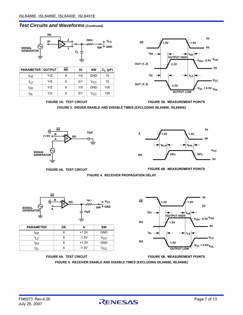
Test Circuits and Waveforms
FIGURE 1. DRIVER VOD AND VOC
FIGURE 2A. TEST CIRCUIT FIGURE 2B. MEASUREMENT POINTS
FIGURE 2. DRIVER PROPAGATION DELAY AND DIFFERENTIAL TRANSITION TIMES
D
DE
DI
VCC
VOD
VOC
R
R
Z
Y
D
DE
DI
VCC
SIGNALGENERATOR
CL = 100pF
RDIFF
Z
Y CL = 100pF
OUT (Y)
3V
0V
tPLH
1.5V1.5V
VOH
VOL
50% 50%
tPHL
OUT (Z)
tPHL
VOH
VOL
50% 50%
tPLH
DIFF OUT (Y - Z)
tR
+VOD
-VOD
90% 90%
tF
10% 10%
DI
SKEW = |tPLH (Y or Z) - tPHL (Z or Y)|
FN6073 Rev.4.00 Page 6 of 13July 26, 2007
ISL8488E, ISL8489E, ISL8490E, ISL8491E
FIGURE 3A. TEST CIRCUIT FIGURE 3B. MEASUREMENT POINTS
FIGURE 3. DRIVER ENABLE AND DISABLE TIMES (EXCLUDING ISL8488E, ISL8490E)
FIGURE 4A. TEST CIRCUIT FIGURE 4B. MEASUREMENT POINTS
FIGURE 4. RECEIVER PROPAGATION DELAY
FIGURE 5A. TEST CIRCUIT FIGURE 5B. MEASUREMENT POINTS
FIGURE 5. RECEIVER ENABLE AND DISABLE TIMES (EXCLUDING ISL8488E, ISL8490E)
Test Circuits and Waveforms (Continued)
D
DE
DI
CL
500Z
Y
VCC
GNDSW
PARAMETER OUTPUT RE DI SW CL (pF)
tHZ Y/Z X 1/0 GND 15
tLZ Y/Z X 0/1 VCC 15
tZH Y/Z X 1/0 GND 100
tZL Y/Z X 0/1 VCC 100
SIGNALGENERATOR
OUT (Y, Z)
3V
0V
1.5V1.5V
VOH
0V2.3V
VOH - 0.5V
tHZ
OUT (Y, Z)
VCC
VOL
2.3VVOL + 0.5V
tLZ
DE
OUTPUT HIGH
OUTPUT LOW
tZL
tZH
SIGNALGENERATOR
RRO
RE
A
B+1.5V
15pF
RO
3V
0V
tPLH
1.5V1.5V
VCC
0V
50% 50%
tPHL
A
1k VCC
GNDSW
PARAMETER DE A SW
tHZ X +1.5V GND
tLZ X -1.5V VCC
tZH X +1.5V GND
tZL X -1.5V VCC
SIGNALGENERATOR
RRO
RE
A
B
15pF
RO
3V
0V1.5V1.5V
VOH
0V1.5V
VOH - 0.5V
tHZ
RO
VCC
VOL
1.5VVOL + 0.5V
tLZ
RE
OUTPUT HIGH
OUTPUT LOW
tZL
tZH
FN6073 Rev.4.00 Page 7 of 13July 26, 2007

ISL8488E, ISL8489E, ISL8490E, ISL8491E
Application InformationRS-485 and RS-422 are differential (balanced) data transmission standards for use in long haul or noisy environments. RS-422 is a subset of RS-485, so RS-485 transceivers are also RS-422 compliant. RS-422 is a point-to-multipoint (multidrop) standard, which allows only one driver and up to 10 (assuming one unit load devices) receivers on each bus. RS-485 is a true multipoint standard, which allows up to 32 one unit load devices (any combination of drivers and receivers) on each bus. To allow for multipoint operation, the RS-485 specification requires that drivers must handle bus contention without sustaining any damage.
Another important advantage of RS-485 is the extended common mode range (CMR), which specifies that the driver outputs and receiver inputs withstand signals that range from +12V to -7V. RS-422 and RS-485 are intended for runs as long as 4000’, so the wide CMR is necessary to handle ground potential differences, as well as voltages induced in the cable by external fields.
Receiver Features
These devices utilize a differential input receiver for maximum noise immunity and common mode rejection. Input sensitivity is ±200mV, as required by the RS-422 and RS-485 specifications.
Receiver input resistance surpasses the RS-422 specification of 4k, and meets the RS-485 “Unit Load” requirement of 12k minimum.
Receiver inputs function with common mode voltages as great as 7V outside the power supplies (i.e., +12V and -7V), making them ideal for long networks where induced voltages are a realistic concern.
All the receivers include a “fail-safe if open” function that guarantees a high level receiver output if the receiver inputs are unconnected (floating).
Receivers easily meet the data rate supported by the corresponding driver. ISL8489E/ISL8491E receiver outputs are three-statable via the active low RE input.
Driver Features
The RS-485/RS-422 driver is a differential output device that delivers at least 1.5V across a 54 load (RS-485), and at least 2V across a 100 load (RS-422). The drivers feature low propagation delay skew to maximize bit width, and to minimize EMI. ISL8489E/ISL8491E driver outputs are three-statable via the active high DE input.
The ISL8488E/ISL8489E driver outputs are slew rate limited to further reduce EMI, and to minimize reflections in unterminated or improperly terminated networks. Data rates on these slew rate limited versions are a maximum of 250kbps. Outputs of ISL8490E/ISL8491E drivers are not limited, so faster output transition times allow data rates of at least 10Mbps.
Data Rate, Cables, and Terminations
Twisted pair is the cable of choice for RS-485/RS-422 networks. Twisted pair cables tend to pick up noise and other electromagnetically induced voltages as common mode signals, which are effectively rejected by the differential receivers in these ICs.
RS-485/RS-422 are intended for network lengths up to 4000’, but the maximum system data rate decreases as the transmission length increases. Devices operating at 10Mbps are limited to lengths of a few hundred feet, while the 250kbps versions can operate at full data rates with lengths in excess of 1000’.
Proper termination is imperative, when using the 10Mbps devices, to minimize reflections. Short networks using the 250kbps versions need not be terminated, but, terminations are recommended unless power dissipation is an overriding concern. In point-to-point, or point-to-multipoint (single driver on bus) networks, the main cable should be terminated in its characteristic impedance (typically 120) at the end farthest from the driver. In multi-receiver applications, stubs connecting receivers to the main cable should be kept as short as possible. Multipoint (multi-driver) systems require that the main cable be terminated in its characteristic impedance at both ends. Stubs connecting a transceiver to the main cable should be kept as short as possible.
Built-In Driver Overload Protection
As stated previously, the RS-485 specification requires that drivers survive worst case bus contentions undamaged. The ISL84xxE devices meet this requirement via driver output short circuit current limits, and on-chip thermal shutdown circuitry.
The driver output stages incorporate short circuit current limiting circuitry which ensures that the output current never exceeds the RS-485 specification, even at the common mode voltage range extremes. Additionally, these devices utilize a foldback circuit which reduces the short circuit current, and thus the power dissipation, whenever the contending voltage exceeds either supply.
In the event of a major short circuit condition, ISL84xxE devices also include a thermal shutdown feature that disables the drivers whenever the die temperature becomes excessive. This eliminates the power dissipation, allowing the die to cool. The drivers automatically reenable after the die temperature drops about 15°. If the contention persists, the thermal shutdown/reenable cycle repeats until the fault is cleared. Receivers stay operational during thermal shutdown.
ESD ProtectionAll pins on these devices include class 3 Human Body Model (HBM) ESD protection structures, but the RS-485 pins (driver outputs and receiver inputs) incorporate advanced structures allowing them to survive ESD events in excess of
FN6073 Rev.4.00 Page 8 of 13July 26, 2007

ISL8488E, ISL8489E, ISL8490E, ISL8491E
±15kV HBM. The RS-485 pins are particularly vulnerable to ESD damage because they typically connect to an exposed port on the exterior of the finished product. Simply touching the port pins, or connecting a cable, can cause an ESD event that might destroy unprotected ICs. These new ESD structures protect the device whether or not it is powered up,
protect without allowing any latch-up mechanism to activate, and without degrading the RS-485 common mode range of -7V to +12V. This built-in ESD protection eliminates the need for board level protection structures (e.g., transient suppression diodes), and the associated, undesirable capacitive load they present.
Typical Performance Curves VCC = 5V, TA = +25°C; Unless Otherwise Specified.
FIGURE 6. DRIVER OUTPUT CURRENT vs DIFFERENTIAL OUTPUT VOLTAGE
FIGURE 7. DRIVER DIFFERENTIAL OUTPUT VOLTAGE vs TEMPERATURE
FIGURE 8. DRIVER OUTPUT CURRENT vs SHORT CIRCUIT VOLTAGE
FIGURE 9. SUPPLY CURRENT vs TEMPERATURE
DIFFERENTIAL OUTPUT VOLTAGE (V)
DR
IVE
R O
UT
PU
T C
UR
RE
NT
(m
A)
0 1 2 3 4 50
10
20
30
40
50
60
70
80
90
-40 0 50 852.0
2.2
2.4
2.6
2.8
3.0
3.2
3.4
3.6
TEMPERATURE (°C)
DIF
FE
RE
NT
IAL
OU
TP
UT
VO
LTA
GE
(V
)-25 25 75
RDIFF = 54
RDIFF = 100
OUTPUT VOLTAGE (V)-7 -6 -4 -2 0 2 4 6 8 10 12
OU
TP
UT
CU
RR
EN
T (
mA
)
-60
-40
-20
0
20
40
60
80
100
120
140
160
-80
-100
-120
Y OR Z = HIGH
Y OR Z = LOW
ISL8490E/ISL8491E
ISL8490E/ISL8491E
ISL8488E/ISL8489E
ISL8488E/ISL8489E
-40 0 50 85TEMPERATURE (°C)
I CC
(µ
A)
-25 25 7550
100
150
200
250
300
350
400
ISL8490E/ISL8491E, DE = X, RE = X
ISL8489E, DE = X, RE = X
ISL8488E
FN6073 Rev.4.00 Page 9 of 13July 26, 2007

ISL8488E, ISL8489E, ISL8490E, ISL8491E
FIGURE 10. DRIVER PROPAGATION DELAY vs TEMPERATURE (ISL8488E/ISL8489E)
FIGURE 11. DRIVER SKEW vs TEMPERATURE (ISL8488E/ISL8489E)
FIGURE 12. DRIVER PROPAGATION DELAY vs TEMPERATURE (ISL8490E/ISL8491E)
FIGURE 13. DRIVER SKEW vs TEMPERATURE (ISL8490E/ISL8491E)
FIGURE 14. DRIVER AND RECEIVER WAVEFORMS, LOW TO HIGH (ISL8488E/ISL8489E)
FIGURE 15. DRIVER AND RECEIVER WAVEFORMS, HIGH TO LOW (ISL8488E/ISL8489E)
Typical Performance Curves VCC = 5V, TA = +25°C; Unless Otherwise Specified.
-40 0 50 85
TEMPERATURE (°C)
-25 25 75
PR
OP
AG
AT
ION
DE
LA
Y (
ns
) tPLHY
tPHLY
tPLHZ
tPHLZ
450
500
550
600
650
700
750
-40 0 50 85
TEMPERATURE (°C)
SK
EW
(n
s)
-25 25 75
|tPLHY - tPHLZ|
|tPHLY - tPLHZ|
|CROSS PT. OF Y AND Z TO CROSS PT. OF Y AND Z|
0
50
100
150
200
250
-40 0 50 85
TEMPERATURE (°C)
-25 25 75
tPLHY
tPHLZ
PR
OP
AG
AT
ION
DE
LA
Y (
ns)
tPLHZ
16
18
20
22
24
26
28
30
tPHLY
-40 0 50 85
TEMPERATURE (°C)
SK
EW
(n
s)
-25 25 75
|tPLHY - tPHLZ|
|tPHLY - tPLHZ|
|CROSS PT. OF Y AND Z TO CROSS PT. OF Y AND Z
0
1
2
3
4
5
TIME (400ns/DIV)0
RE
CE
IVE
R O
UT
PU
T (
V)
3
4
1
2
RDIFF = 54, CL = 100pF
0
DR
IVE
R O
UT
PU
T (
V)
0
5
DR
IVE
R I
NP
UT
(V
)
DI
RO
Y
Z
5
TIME (400ns/DIV)0
RE
CE
IVE
R O
UT
PU
T (
V)
3
4
1
2
RDIFF = 54, CL = 100pF
0
DR
IVE
R O
UT
PU
T (
V)
0
5D
RIV
ER
IN
PU
T (
V)
DI
RO
Y
Z
5
FN6073 Rev.4.00 Page 10 of 13July 26, 2007

ISL8488E, ISL8489E, ISL8490E, ISL8491E
Die Characteristics
SUBSTRATE POTENTIAL (POWERED UP):
GND
TRANSISTOR COUNT:
518
PROCESS:
Si Gate BiCMOS
FIGURE 16. DRIVER AND RECEIVER WAVEFORMS, LOW TO HIGH (ISL8490E/ISL8491E)
FIGURE 17. DRIVER AND RECEIVER WAVEFORMS, HIGH TO LOW (ISL8490E/ISL8491E)
Typical Performance Curves VCC = 5V, TA = +25°C; Unless Otherwise Specified.
TIME (20ns/DIV)0
RE
CE
IVE
R O
UT
PU
T (
V)
3
4
1
2
RDIFF = 54, CL = 100pF
0
5
DR
IVE
R O
UT
PU
T (
V)
0
5
DR
IVE
R IN
PU
T (
V)
DI
RO
Y
Z
TIME (20ns/DIV)0
RE
CE
IVE
R O
UT
PU
T (
V)
3
4
1
2
RDIFF = 54, CL = 100pF
0
5
DR
IVE
R O
UT
PU
T (
V)
0
5
DR
IVE
R IN
PU
T (
V)
DI
RO
Y
Z
FN6073 Rev.4.00 Page 11 of 13July 26, 2007

ISL8488E, ISL8489E, ISL8490E, ISL8491E
FN6073 Rev.4.00 Page 12 of 13July 26, 2007
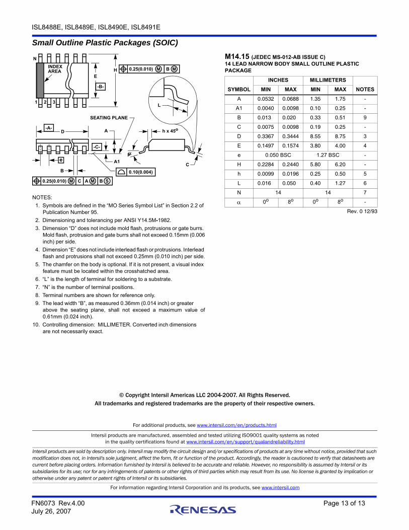
Small Outline Plastic Packages (SOIC)
INDEXAREA
E
D
N
1 2 3
-B-
0.25(0.010) C AM B S
e
-A-
L
B
M
-C-
A1
A
SEATING PLANE
0.10(0.004)
h x 45°
C
H 0.25(0.010) BM M
NOTES:
1. Symbols are defined in the “MO Series Symbol List” in Section 2.2 of Publication Number 95.
2. Dimensioning and tolerancing per ANSI Y14.5M-1982.
3. Dimension “D” does not include mold flash, protrusions or gate burrs. Mold flash, protrusion and gate burrs shall not exceed 0.15mm (0.006inch) per side.
4. Dimension “E” does not include interlead flash or protrusions. Inter-lead flash and protrusions shall not exceed 0.25mm (0.010 inch) perside.
5. The chamfer on the body is optional. If it is not present, a visual index feature must be located within the crosshatched area.
6. “L” is the length of terminal for soldering to a substrate.
7. “N” is the number of terminal positions.
8. Terminal numbers are shown for reference only.
9. The lead width “B”, as measured 0.36mm (0.014 inch) or greater above the seating plane, shall not exceed a maximum value of0.61mm (0.024 inch).
10. Controlling dimension: MILLIMETER. Converted inch dimensions are not necessarily exact.
M8.15 (JEDEC MS-012-AA ISSUE C)8 LEAD NARROW BODY SMALL OUTLINE PLASTIC PACKAGE
SYMBOL
INCHES MILLIMETERS
NOTESMIN MAX MIN MAX
A 0.0532 0.0688 1.35 1.75 -
A1 0.0040 0.0098 0.10 0.25 -
B 0.013 0.020 0.33 0.51 9
C 0.0075 0.0098 0.19 0.25 -
D 0.1890 0.1968 4.80 5.00 3
E 0.1497 0.1574 3.80 4.00 4
e 0.050 BSC 1.27 BSC -
H 0.2284 0.2440 5.80 6.20 -
h 0.0099 0.0196 0.25 0.50 5
L 0.016 0.050 0.40 1.27 6
N 8 8 7
0° 8° 0° 8° -
Rev. 1 6/05
FN6073 Rev.4.00 Page 13 of 13July 26, 2007
ISL8488E, ISL8489E, ISL8490E, ISL8491E
Intersil products are manufactured, assembled and tested utilizing ISO9001 quality systems as notedin the quality certifications found at www.intersil.com/en/support/qualandreliability.html
Intersil products are sold by description only. Intersil may modify the circuit design and/or specifications of products at any time without notice, provided that such modification does not, in Intersil's sole judgment, affect the form, fit or function of the product. Accordingly, the reader is cautioned to verify that datasheets are current before placing orders. Information furnished by Intersil is believed to be accurate and reliable. However, no responsibility is assumed by Intersil or its subsidiaries for its use; nor for any infringements of patents or other rights of third parties which may result from its use. No license is granted by implication or otherwise under any patent or patent rights of Intersil or its subsidiaries.
For information regarding Intersil Corporation and its products, see www.intersil.com
For additional products, see www.intersil.com/en/products.html
© Copyright Intersil Americas LLC 2004-2007. All Rights Reserved.All trademarks and registered trademarks are the property of their respective owners.
Small Outline Plastic Packages (SOIC)
NOTES:
1. Symbols are defined in the “MO Series Symbol List” in Section 2.2 of Publication Number 95.
2. Dimensioning and tolerancing per ANSI Y14.5M-1982.
3. Dimension “D” does not include mold flash, protrusions or gate burrs. Mold flash, protrusion and gate burrs shall not exceed 0.15mm (0.006inch) per side.
4. Dimension “E” does not include interlead flash or protrusions. Interlead flash and protrusions shall not exceed 0.25mm (0.010 inch) per side.
5. The chamfer on the body is optional. If it is not present, a visual index feature must be located within the crosshatched area.
6. “L” is the length of terminal for soldering to a substrate.
7. “N” is the number of terminal positions.
8. Terminal numbers are shown for reference only.
9. The lead width “B”, as measured 0.36mm (0.014 inch) or greater above the seating plane, shall not exceed a maximum value of0.61mm (0.024 inch).
10. Controlling dimension: MILLIMETER. Converted inch dimensions are not necessarily exact.
INDEXAREA
E
D
N
1 2 3
-B-
0.25(0.010) C AM B S
e
-A-
L
B
M
-C-
A1
A
SEATING PLANE
0.10(0.004)
h x 45o
C
H
µ
0.25(0.010) BM M
M14.15 (JEDEC MS-012-AB ISSUE C)14 LEAD NARROW BODY SMALL OUTLINE PLASTIC PACKAGE
SYMBOL
INCHES MILLIMETERS
NOTESMIN MAX MIN MAX
A 0.0532 0.0688 1.35 1.75 -
A1 0.0040 0.0098 0.10 0.25 -
B 0.013 0.020 0.33 0.51 9
C 0.0075 0.0098 0.19 0.25 -
D 0.3367 0.3444 8.55 8.75 3
E 0.1497 0.1574 3.80 4.00 4
e 0.050 BSC 1.27 BSC -
H 0.2284 0.2440 5.80 6.20 -
h 0.0099 0.0196 0.25 0.50 5
L 0.016 0.050 0.40 1.27 6
N 14 14 7
0o 8o 0o 8o -
Rev. 0 12/93