is split manufacturing secure?
TRANSCRIPT
Is Split Manufacturing Secure?Jeyavijayan (JV) Rajendran†, Ozgur Sinanoglu‡, and Ramesh Karri†
†Polytechnic Institute of New York University, ‡New York University – Abu DhabiEmail: [email protected], [email protected], [email protected]
Abstract— Split manufacturing of integrated circuits (IC) isbeing investigated as a way to simultaneously alleviate the costof owning a trusted foundry and eliminate the security risksassociated with outsourcing IC fabrication. In split manufactur-ing, a design house (with a low-end, in-house, trusted foundry)fabricates the Front End Of Line (FEOL) layers (transistorsand lower metal layers) in advanced technology nodes at anuntrusted high-end foundry. The Back End Of Line (BEOL)layers (higher metal layers) are then fabricated at the designhouse’s trusted low-end foundry. Split manufacturing is consid-ered secure (prevents reverse engineering and IC piracy) as ithides the BEOL connections from an attacker in the FEOLfoundry. We show that an attacker in the FEOL foundry canexploit the heuristics used in typical floorplanning, placement, androuting tools to bypass the security afforded by straightforwardsplit manufacturing. We developed an attack where an attackerin the FEOL foundry can connect 96% of the missing BEOLconnections correctly. To overcome this security vulnerability insplit manufacturing, we developed a fault analysis-based defense.This defense improves the security of split manufacturing bydeceiving the FEOL attacker into making wrong connections.
I. INTRODUCTION
Integration of digital, analog, radio frequency, photonicand other devices into a complex System on Chip (SoC) hasbeen demonstrated [2]. More recently, sensors, actuators, andbiochips are also being integrated into these already powerfulSoCs. On one hand, SoC integration has been enabled byadvances in mixed system integration and the increase inthe wafer sizes (currently about 300 mm and projected tobe 450mm by 2018 [2]). It has also reduced the cost perchip of such SOCs. On the other hand, support for multiplecapabilities and mixed technologies has increased the cost ofownership of advanced foundries. For instance, the cost ofowning a foundry will be $5 billion in 2015 [9]. Consequently,only large commercial foundries now manufacture such highperformance, mixed system SoCs especially at the advancedtechnology nodes [10]. Absent the economies of scale, manyof the design companies cannot afford owning and acquiringexpensive foundries and hence outsource their design fabrica-tion to these “one-stop-shop” foundries1.
Globalization of Integrated Circuits (IC) design flow hasled to several security vulnerabilities. If a design is fabricatedin a foundry that is not under the direct control of the (fabless)design house, attacks such as reverse engineering, maliciouscircuit modification and Intellectual Property (IP) piracy arepossible [10]. An attacker, anywhere in this design flow, canreverse engineer the functionality of an IC/IP, and then stealand claim ownership of the IP. An untrusted IC foundry mayoverbuild ICs and sell them illegally. Finally, rogue elementsin the foundry may insert malicious circuits (hardware trojans)into the design without the designer’s knowledge [8], [17].Because of these attacks, the semiconductor industry loses $4billion annually [19].
A. Split manufacturingLeading fabless semiconductor companies such as AMD
and research agencies such as Intelligence Advanced ResearchProjects Agency (IARPA) have proposed split manufacturingto thwart such attacks [10], [11]. In split manufacturing, thelayout of the design is split into the Front End Of Line (FEOL)layers and Back End Of Line (BEOL) layers which are thenfabricated separately in different foundries. The FEOL layers
1companies that do not own their foundry are termed ‘fabless’ designhouses.978-3-9815370-0-0/DATE13/ c©2013 EDAA
Via
Wire
}}}}Top metal layers
(BEOL)
Intermediate
metal layers
(BEOL)
Lower metal
layers
(FEOL)
Transistors
(FEOL)
Layer Pitch (nm)M10 1600M9 1600M8 800M7 800M6 280M5 280M4 280M3 140M2 140M1 130Poly 125
(a) (b)
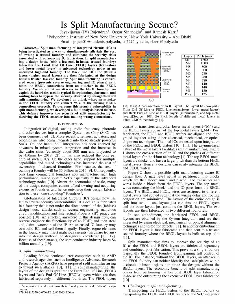
Fig. 1: (a) A cross-section of an IC layout. The layout has two parts:Front End Of Line or FEOL layers(transistors, lower metal layers)and Back End Of Line or BEOL layers (intermediate, and top metallayers)[Source: [10]]. (b) Pitch length of different metal layers in45nm CMOS technology [1].
consist of transistors and other lower metal layers (≤M4) andthe BEOL layers consist of the top metal layers (¿M4). Postfabrication, the FEOL and BEOL wafers are aligned and inte-grated together using either electrical, mechanical, or opticalalignment techniques. The final ICs are tested upon integrationof the FEOL and BEOL wafers [10], [11]. The asymmetricalnature of the metal layers facilitates split manufacturing. Figure1 shows the cross-section of an IC and the pitches of differentmetal layers for the 45nm technology [1]. The top BEOL metallayers are thicker and have a larger pitch than the bottom FEOLmetal layers. Hence, a designer can easily integrate the BEOLand FEOL wafers.
Figure 2 shows a possible split manufacturing aware ICdesign flow. A gate level netlist is partitioned into blockswhich are then floorplanned and placed. The transistors andwires inside a block form the FEOL layers. The top metalwires connecting the blocks and the IO ports form the BEOLlayers. The BEOL and FEOL wires are assigned to differentmetal layers and routed such that the wiring delay and routingcongestion are minimized. The layout of the entire design issplit into two — one layout just contains the FEOL layersand the other layout just contains the BEOL layers. The twolayouts are then fabricated in two different foundries.
In one embodiment, the fabricated FEOL and BEOLlayouts are obtained by the System Integrator, and are thenintegrated by using electrical, mechanical, or optical alignmenttechniques and tested for defects. [11]. In another embodiment,the FEOL layout is first fabricated and then sent to a trustedsecond foundry where the BEOL layout is built on top of it[11].
Split manufacturing aims to improve the security of anIC as the FEOL and BEOL layers are fabricated separatelyand combined post fabrication. This prevents a single foundry(especially the FEOL foundry) from gaining full control ofthe IC. For instance, without the BEOL layers, an attacker inthe FEOL foundry can neither identify the ‘safe’places withina circuit to insert trojans nor pirate the designs without theBEOL layers. The economic benefit of split manufacturingcomes from performing the low cost BEOL layer fabricationin-house and outsourcing the expensive FEOL layer fabrication[10]
B. Challenges in split manufacturingTransporting the FEOL wafers to the BEOL foundry or
transporting the FEOL and BEOL wafers to the SoC integrator

Fig. 2: Split manufacturing aware design flow.
may present a challenge; these wafers are thin and might crackor delaminate during transportation. Alignment of the FEOLand BEOL layers and increase in die area to accommodatealignment structures present another challenge. Split manufac-turing may also affect the signal integrity, timing of the signalsthat span the FEOL and BEOL layers, and other design-for-manufacturability aspects. While several research projects fromresearch agencies such as IARPA [10] and companies such asAMD [11] focus on addressing these challenges and make itfeasible to reap the benefits of split manufacturing, we showthat split manufacturing is inherently insecure.
C. ContributionsIn this work, we address the following questions:1) Is split manufacturing inherently secure?2) If not, how can it be compromised?3) How can it be strengthened?
The security offered by split manufacturing stems from thefact that the attacker in the FEOL foundry cannot determinethe missing BEOL connections. We perform a security anal-ysis of split manufacturing and show how an attacker candetermine the missing BEOL connections by using knowledgeof the FEOL connections. We propose proximity attack thatexploits the vulnerabilities introduced by the physical designtools (floorplanning, placement, and routing tools). Then, theattacker can determine the missing BEOL connections andhe can either pirate the design or insert trojans into it. Wepropose a defense to thwart the proximity attack by deceivingan attacker to make wrong BEOL connections. This techniqueinvolves the adoption of IC testing principles (fault excitation,fault propagation, and fault masking) to swap partition pinsand improve security of split manufacturing.
II. SECURITY ANALYSIS OF SPLIT MANUFACTURING
A. Threat modelThe attacker is in the offshore foundry that manufactures
the FEOL part. Since the attacker has the GDSII layout file ofthe design, he/she can reverse engineer it and obtain the gate-level netlist. Such reverse engineering techniques have beendemonstrated in [21]. The attacker in the FEOL foundry gainsknowledge about most of the design (the transistors and thelower metal layers) except for the missing BEOL connections.Once the attacker determines these missing BEOL connections,he/she can reconstruct the original design.
B. Motivational exampleConsider the ISCAS-85 combinational logic benchmark
circuit, C17 shown in Figure 3. This design has five inputs(I1-I5) and two outputs (O1, O2). It is partitioned into twopartitions – A (light colored) and B (dark colored). PartitionA has four inputs (inputs of G1, G2, and G3) and two outputs(outputs of G7 and G9). Partition B has three inputs (inputs ofG4, G5, and one input of G10) and one output (output of G10).Traditionally, the wires within a partition (local wires exceptVdd and clock) are assigned to lower metal layers. The wiresthat span the partitions and I/O ports are assigned to highermetal layers. This makes the routing easier [20]. The netsconnecting the input ports I1-I5 to the corresponding inputsof the gates G1-G5 use the BEOL layers. The nets connectingthe output of gates G9 and G10 to output ports O1 and O2,
G2
G1
G5
G4
G3
G8
G7
G6
G9
G10
Partition A
Partition B
I4
I3
I5
I1
I2 O1
O2
1
2
3
Fig. 3: The C17 benchmark circuit. The violet (light) and green(dark) regions represent partitions A and B, respectively. The outputof G7 goes between the partitions. Thin lines denote FEOL netswhile the thick lines denote the BEOL nets. 1© Target pin PI1,IO,in, 2©corresponding candidate pin PI1,A,in, and 3© swapping pin PI2,IO,in.
respectively, use the BEOL layers. The net that connects theoutput of G7 to one of the inputs of G10 also uses the BEOLlayer.
C. TerminologyIn this paper, PNet,Partition,Direction denotes a partition pin or
an IO port. Net is the name of the wire in the original design.Partition represents either the partitions A or B or the IOport. Direction of a pin can be either in or out. Consider anet X in the original design which connects a gate in PartitionA to another gate in Partition B. The corresponding partitionpins on the partition boundaries of Partition A and PartitionB are denoted as PX,A,out and PX,B,in, respectively.
A target pin is an output pin of a partition or an input portof the design from which a signal originates. A candidate pinis an input pin of a partition or an output port of the designat which a signal terminates. Consider the C17 circuit shownin Figure 3. Pin PI1,IO,in is the target pin and pin PI1,A,in is itscorresponding candidate pin. A target pin in a partition willbe swapped with another pin in the same partition referred toas swapping pin. In Figure 3, pin PI2,IO,in is the swapping pinfor target pin PI1,IO,in.
Every missing BEOL connection is a net that connects atarget pin and its corresponding candidate pin. A target pin hasmany candidate pins but the attacker is trying to determine thecorrect candidate pin for that target pin with the followingobjective: If she can connect every target pin with its correctcandidate pin, she can recover the original design.
D. Proximity attackThe proposed attack is based on the heuristic that floor-
planning and placement (F&P) tools place the partitions closeby and orient the partitions so as to reduce the wiring (delay)between the pins to be connected [20]. This heuristic of mostF&P tools constitute a security vulnerability that can beexploited by an attacker in the FEOL foundry who does nothave access to the BEOL layers.
Consider a target pin, PX,A,out, and its corresponding can-didate pin, PX,B,in. F&P tools will try to place PX,A,out closerto PX,B,in than to any other partition pin in Partition B. Anattacker may then recover the netlist of the original design byconnecting every target pin to its closest candidate pin. This isreferred to as the proximity attack. This attack uses the hintsprovided by the F&P tools that are explained below:

Hint 1 – Input-output relationships: An input partitionpin (candidate pin) will be connected either to an output pinof another partition or to an input port of the IC (target pin).Input partition pins are usually connected to the poly layer andoutput partition pins usually emanate from the diffusion layer.
Consider the partition pin PI1,A,in of the partitioned F&PC17 benchmark circuit in Figure 3. This is an input pin forPartition A. This pin can be connected only to pins PI1,IO,in,PI2,IO,in, PI3,IO,in, PI4,IO,in, PI5,IO,in, and PG10,B,out, reducing thepossible candidate pins from 10 to 6.
G1
G2
G1
G2
G3G3
(a) (b)
Fig. 4: Typical fan-out push performed by F&P tools.
Hint 2 – Unique inputs per partition: A net in a designwill be connected to only one input pin of a partition. If a netacts as an input for multiple gates within that partition, thefan-out node is usually placed within the partition that it feedsinto.
Consider the partition in Figure 4. Partition A has twooutput pins PG1,A,out1 and PG1,A,out2 and Partition B has twoinput pins PG1,B,in1 and PG1,B,in2. On pushing the fan-out nodeinto Partition B, as shown in Figure 4(b), the number of inputand output pins in Partition A and Partition B, respectively,is reduced by one. This observation reduces the number ofpossible connections from 2N2
to N! for N missing connections,as every target pin will have a unique candidate pin.
Hint 3 – Combinational loops: With the exception ofring oscillators, flip-flops, and latches, combinational loopsare rare in a design. Furthermore, ring oscillators, flip-flops,and latches are contained within a single partition and areeasily identifiable due to their standard structure. Therefore,an attacker does not need to consider a pin as a candidate pin,if it forms a combinational loop with the target pin.
Consider the partitions in Figure 3. After connecting thetarget pin PG7,A,out to candidate PG7,B,in, an attacker will notconsider the output pin PG10,B,out as a possible candidate pinfor the target pins PI2,A,in, PI3,A,in, and PI4,A,in because PG10,B,outwill form a combinational loop when connected to any one ofthese pins.
An attacker can find the correct candidate pin for a targetpin by identifying the closest pin from the list of possiblecandidate pins. As mentioned before, this heuristic is based onthe fact that F&P tools try to place two partition pins, whichare to be connected by a BEOL layer, as close as possible toeach other to reduce the wiring overhead. So, an attacker canconnect the two closest pins in different partitions hoping thatF&P tools must have placed them close to each other.
Consider the locations of partition pins and IO ports ofthe F&P C17 benchmark as shown in Table I. Consider theinput port PI1,IO,in which is connected to pin PI1,A,in in partitionA. The locations of PI1,IO,in and PI1,A,in are (0,6) and (1,6),respectively. The distance between these two pins is 1 unit.Now, consider another input port PI3,IO,in. The distance betweenPI3,IO,in and PI1,A,in is 1.414 units. Thus, the closest possible pin
TABLE I: X-Y coordinates of the pins in partitions A and B andIO ports of F&P C17 design. The coordinates are shown as absoluteunits for ease of understanding.
Partition A Partition B Input & OutputPin XY Pin XY Port XY
location location locationPI1,A,in (1,6) PI4,B,in (1,2) PI1,IO,in (0,6)PI2,A,in (9,5) PI5,B,in (1,0) PI2,IO,in (10,6)PI3,A,in (1,5) PG7,B,in (7,2) PI3,IO,in (0,5)PI4,A,in (1,4) PG10,B,out (7,0) PI4,IO,in (0,4)
PG9,A,out (9,4) PI5,IO,in (0,0)PO1,IO,out (10,5)PO2,IO,out (8,0)
to PI1,A,in is PI1,IO,in. Hence, an attacker will connect these twopins in the netlist and obtain the missing BEOL connection.Similarly, he can connect all the other partition pins with theirclosest pins and reconstruct the original design.
E. Proximity attack algorithmInput : FEOL layersOutput: Netlist with BEOL connections
1 Reverse engineer FEOL layers and obtain the partitions;2 while Unassigned partition pins or ports exist do3 Select an arbitrary unassigned input pin or an output port
as a TargetP in;4 ListOfCandidateP ins =
BuildCandidatePinsList(TargetP in);5 Select CandidateP in from ListOfCandidateP ins
that is closest to TargetP in;6 Connect TargetP in and CandidateP in;7 Update netlist;8 end9 Return netlist;
10 —————————————————————11 BuildCandidatePinsList(TargetPin)
Input : TargetP in PX,i,inOutput: Candidate pins for TargetP in
12 CandidatePins = Unassigned output pins of other partitions +unassigned input ports of the design;
13 For each PinJ ∈ CandidatePins do14 if CombinationalLoop(TargetPin, PinJ) then15 CandidatePins -= PinJ;16 end17 end18 Return CandidatePins;19 —————————————————————Algorithm 1: Proximity attack on split manufacturing
Algorithm 1 describes the steps involved in the proximityattack. The input to the algorithm is the FEOL layer informa-tion and the goal is to reconstruct the netlist by identifyingthe missing BEOL connections2. The algorithm chooses anarbitrary TargetP in from the unassigned partition input pinsand output ports, creates its list of possible CandidateP ins,and connects it to the closest pin in this list. The netlist isthen updated. This procedure is repeated until all the missingconnections are made. Candidate pins for a target pin arechosen based on the observations 1–3. After executing thisalgorithm, the attacker obtains the missing BEOL connectionsand, consequently, the original design.
III. SECURE SPLIT MANUFACTURING
One technique to overcome proximity attack is to rearrangethe partition pins such that a pin PX,A,out will no longer be theclosest pin to PX,B,in. An attacker performing proximity attackwill be deceived into making the wrong BEOL connections,i.e., PX,B,in will be connected with PY,A,out instead of PX,A,out.
Consider the F&P C17 circuit. Before swapping, pinPG7,A,out is close to pin PG7,B,in. Hence, an attacker will connectthem. If the pins PG7,A,out and PG9,A,out are swapped, thenPG9,A,out will be close to PG7,B,in. Therefore, an attacker willconnect these two pins, thereby making a wrong connection.
Objective: Sufficient number of pins have to be swappedsuch that the functionality of the deceiving netlist3 differsfrom that of the original netlist. This functional differencecan be quantified by the Hamming distance between theoutputs of the original netlist and the deceiving netlist. Ifit is 0%, then the attacker is able to retrieve the originaldesign. If it is 100%, then the attacker is able to retrievethe design that is the exact complement of original design.Hence, ideally, the Hamming distance should be 50% wherea different set of the outputs are corrupted for different inputvectors. A designer can stop swapping pins when the Hamming
2The netlist of the FEOL layout [21] can be obtained from the GDSII netlistof the FEOL part. Several tools for this purpose exist [7].
3Deceiving netlist is the netlist that the defender manipulates by swappingthe pins.

G1
G2
G3
1
2
X
Y
(a)
G2
G3
1
2
G5
G1 G4
(b)
G21
G4
G1 G3
2
(c)
Fig. 5: IC testing principles applied to split manufacturing: (a) Pinthat has a logical value opposite to that of the swapped pin ispreferred. 1© Values at PG1,A,out and PG2,A,out differ only when X=Y=0;2© Values at PG2,A,out and PG3,A,out differ in two cases: X=1, Y=0
and X=0, Y=1. Thus, PG3,A,out is selected as the swapping pin forPG2,A,out. (b) If PG1,A,out is selected as the swapping pin for PG2,A,out,the wrong value will propagate only when the other input of G4 is1. However, if PG3,A,out is selected as the swapping pin, the buffer,G5, will always propagate the wrong value. (c) The logical errorintroduced by swapping PG1,A,out and PG2,A,out is canceled by swappingPG3,B,out and PG4,B,out.
distance between the outputs of the original netlist and thedeceiving netlist reaches 50%. Finding the best rearrangementfor N pins of a partition might take N! computations andthis is computationally expensive. We will consider pair-wiseswapping of pins. Pair-wise swapping of pins results in O(N2)computations.
Constraints on pin swapping: Not all pins can beswapped with all other pins. The target pin and swapping pintogether should pass the basic tests presented as hints in theprevious section. Otherwise, the attacker might omit it fromfurther consideration. Therefore, for a target pin, a swappingpin should
• be an output pin of the partition where the target pinresides,
• not be connected to the partition where the candidatepin resides, and
• not form a combinational loop with a candidate pinon connecting with it.
A. IC testing principles for split manufacturingTo find a swapping pin for a target pin, similar to an at-
tacker, the defender can build the list of candidate pins for thattarget pin. Then, he/she can randomly select the swapping pinfrom that list. Unfortunately, such random selections might notguarantee that the attacker will get a wrong output on makinga wrong connection. Hence, we use IC testing principles [5],to select the swapping pin for a target pin in order to achievethe 50% Hamming distance objective.
Scenario 1 – Commutativity: Consider the scenariowhere the swapping pin and the target pin are the two inputsof the same gate that implements a commutative operation,and neither of them act as an input of any other gate. Onswapping these two pins, the logical functionality remains thesame despite the wrong connection.
Scenario 2 – Fault activation: The logical values atthe swapping pin and target pin should differ for most of theinput patterns. If their logical values are the same for most ofthe input patterns, then the resulting design, even with wrongconnections, will still produce mostly correct outputs. This issimilar to fault activation in IC testing where, in order to detecta stuck-at-fault at a node, the node should be justified to thevalue that is the opposite of the stuck-at value [5]. Thus, a pinthat has a logical value opposite to that of the target pin formost of the input patterns should be selected as the swappingpin.
Consider the partitioned design shown in Figure 5 (a). IfPG1,A,out is selected as the swapping pin for target pin PG2,A,out,the logical values at the pins differ when X=Y=0. If PG3,A,out isselected as the swapping pin for target pin PG2,A,out, the logicalvalues at the pins differ in two cases: X=1, Y=0 and X=0, Y=1.Thus, PG3,A,out is preferred over PG1,A,out.
Scenario 3: Fault propagation: Pins should be swappedsuch that a wrong value activated by the swap can easily prop-agate to one or more outputs and corrupt them. If the swappingpin results in a wrong value which does not propagate to oneor more outputs, then that swap is ineffective. Once again, thisis similar to the fault propagation concept in IC testing wherethe effect of a fault has to propagate to one or more outputsfor detection [5]. Thus, pins should be swapped such that theeffect of swapping propagates to one or more outputs.
Consider the partitioned design shown in Figure 5 (b). IfPG1,A,out is selected as the swapping pin for PG2,A,out, the wrongvalue will propagate only when the other input of G4 is 1.However, if PG3,A,out is selected as the swapping pin, the buffer,G5, will always propagate the wrong value. Thus, PG3,A,out ispreferred over PG1,A,out.
Scenario 4: Fault masking: Sometimes, logical valuescorrupted by swapping pins in partition A can be restored totheir original value because of swapping pins in partition B.This is similar to fault masking in IC testing where the effectof one fault is restored by the effect of another fault [5].
Consider the partitioned design shown in Figure 5 (c). Thelogical error introduced by swapping PG1,A,out and PG2,A,out iscanceled by swapping PG3,B,out and PG4,B,out.
Thus, random selection of a swapping pin might notguarantee a wrong output for an attacker while increasing thewire length for the defender. Hence, we propose a judiciousswapping technique based on fault analysis, which is proposedin [16].
Input : PartitionsOutput: List of target and swapping pins
1 ListofTargetP ins = φ;2 ListofSwappingP ins = φ;3 ListofUntouchedP ins = All partition pins and I/O ports;4 while Untouched output partition pins or input ports exist do5 For each UntouchedP in do6 SwappingP ins =
BuildSwappingPinsList(UntouchedP in);7 For each SwappingP in ∈ SwappingP ins do8 Compute
FaultImpactUntouchedPin,SwappingPin;9 end
10 end11 Find the TargetP in and SwappingP in with the highest
FaultImpact from its SwappingP ins;12 ListofTargetP ins += TargetP in;13 ListofSwappingP ins += SwappingP ins;14 ListofUntouchedP ins -= TargetP in;15 ListofUntouchedP ins -= SwappingP in;16 Swap TargetP in and SwappingP in;17 Update netlist;18 end19 Return ListofTargetP ins and ListofSwappingP ins;20 —————————————————————21 BuildSwappingPinsList(TargetP in);
Input : TargetP in PX,i,outOutput: SwappingP ins for TargetP in
22 SwappingP ins = Other untouched output pins in partition‘i’;
23 For each PinJ ∈ SwappingP ins do24 if CombinationalLoop(TargetP in, PinJ) then25 SwappingP ins -= PinJ;26 end27 end28 Return SwappingP ins;29 —————————————————————Algorithm 2: Fault analysis-based swapping of pins tothwart proximity attack
B. Defense: Fault-analysis based pin swappingInstead of randomly selecting the swapping pin, the pin
that affects most of the outputs for most of the input patternson swapping is selected. This accounts for fault activation,propagation, and masking scenarios. We define the fault impact

0%
10%
20%
30%
40%
50%
60%
70%
80%
0 10 20 30 40 50 60 70 80 90 100 110 120 130 140 150 160 170
Ham
min
g D
ista
nce
Number of swaps
C17 (1)C432 (4)
C499 (14)C880 (8)
C1355 (18)C1908 (10)C3540 (8)
C5315 (72)C7552 (49)
Fig. 6: Hamming distance between the outputs of original designand the design obtained by swapping partition pins based on faultanalysis technique. The number of swaps required to achieve the 50%Hamming distance is shown in parenthesis next to the circuit name.
metric, to select a swapping pin Y for a target pin X ,
Fault impactX,Y =
# of test patterns∑i=1
# of corrupted outputs
We swap the target pin X with the swapping pin Y in thenetlist and identify the cumulative sum of the corrupted outputbits over a set of random test patterns. Fault impact quantifiesthe effect of swapping on the outputs of the design.
Pins can be swapped based on the fault impact metricas shown in Algorithm 2. For an untouched pin (all out-put partition pins and input ports), a list of swapping pins,SwappingP ins, is built using the observations 1–3 in SectionII. Fault impact metric is used to select the swapping and targetpins. The selected pins are then swapped and the netlist isupdated. The above steps are repeated until all the partitionpins and input ports are swapped or the Hamming distancevalue reaches 50%.
IV. RESULTS
A. Experimental setupThe proposed technique was evaluated using ISCAS-85
combinational benchmark circuits4. Each circuit was par-titioned into two partitions using the hMETIS tool [18].Floorplanning, placement, and routing were performed usingCadence SoC Encounter tool [6] for 45nm CMOS technology.The location of the partition pins and IO ports were obtainedusing the same tool. We used the HOPE fault simulation tool[13] to calculate the fault impact metric by applying 1000random input patterns. The Hamming distance between theoutput of the original design and the design reconstructed usingthe proximity attack technique was determined by applying1000 random input patterns. The defender stops swappingpins once he/she reaches the 50% Hamming distance betweenthe original netlist and the deceiving netlist constructed byswapping pins. In case of designs where 50% Hammingdistance was not achieved, he/she swaps all the pins.
B. Required number of swapsThe purpose of swapping pins is to ensure that an attacker
on performing a proximity attack reconstructs an incorrectdesign, i.e., the reconstructed design produces wrong outputsfor most of the inputs. The Hamming distance metric notonly quantifies the tendency of a design to produce a wrongoutput but also quantifies how many output bits are corrupted.Figure 6 shows the Hamming distance between the outputsof the original design and the deceiving netlist obtained afterswapping partition pins based on the proposed fault analysis.
4The physical design benchmarks were not used as they lack informationabout the functionality of the gates, which is important to analyze theeffectiveness of the proposed techniques in producing a wrong output.
Different benchmark circuits have different numbers ofpartition pins. Thus, only a limited number of swaps is possiblein a circuit. In addition, based on the order of swapping,some partition pins might not have candidate pins due tothe observations 1–3 in Section II. For instance, some ofthe swapping pins might form a combinational loop with thecandidate pin, leaving no swapping possibilities.
Fault analysis-based swapping achieves at least 50% Ham-ming distance for all the benchmarks. This is because, itaccounts for the fault activation, propagation, and maskingeffects in pin-swap selections. Furthermore, the curves aresteep in fault analysis-based swapping. This indicates that faultanalysis-based swapping will take a small number of swaps toachieve the 50% Hamming distance mark.
C. Attack metric: Number of correct connections
60
65
70
75
80
85
90
95
100
C17 C432 C499 C880 C1355 C1908 C3540 C5315 C7552
% o
f co
rre
ct
co
nn
ectio
ns
No defense + Proximity connections attackFault-analysis swap defense + Proximity connections attack
Fig. 7: Percentage of partition pins and IO ports that are correctlyconnected by an attacker using proximity attack.
Naturally, an attacker tries to make as many correct con-nections as possible. The number of correct connections ina design reconstructed by the attacker will determine theeffectiveness of the proximity attack. Figure 7 shows thepercentage of partition pins and IO ports that are correctlyconnected by an attacker using proximity attack.
In case of ‘No defense + Proximity connections attack’, theaverage number of correct connections is 96%. In case of theC17 benchmark, the attacker is able to make all the connectionscorrectly. This verifies our earlier claim that F&P tools placepins, which will be connected in BEOL, closer to each otherand indicates that straightforward split manufacturing can beeasily compromised. In case of ‘Fault-analysis swap defense+ Proximity connections attack’, the attacker connects 87%of the pins correctly because only a small number of pinswere swapped; for most of the designs at most 20 pins wereswapped. However, the effectiveness of the remaining 13% ofwrong connections will be explained below.
D. Defense metric: Hamming distance of designs recon-structed by the attacker
Figure 8 depicts the Hamming distance between the outputsof the original design and the design reconstructed usingproximity attack. When proximity attack is performed, theHamming distance between the outputs of the original andreconstructed designs reduces which highlights the effective-ness of the proposed attack. This is particularly evident in thecase where no defense is used.
In case of ‘No defense + Proximity connections attack’, theaverage Hamming distance is around 10% except for C7552circuit. In this circuit, there are more number of I/O portsshared between the two partitions and are placed at equidistantlocations. This prevented the attacker from making the correctconnections, resulting in a higher Hamming distance. However,for most of the benchmark circuits, the Hamming distancevalue of the design reconstructed by the attacker is less than6%. Thus, an attacker almost determines the functionality ofthe design correctly using this attack. Consequently, he/she

0
10
20
30
40
50
60
C17 C432 C499 C880 C1355 C1908 C3540 C5315 C7552
Ha
mm
ing
Dis
tan
ce
(%
)No defense + Proximity connections attack
Fault-analysis swap defense + Proximity connections attack
Fig. 8: Hamming distance between the outputs of the original designand the design reconstructed using proximity attack.
obtains a design which is almost an equivalent to the originaldesign. This necessitates the need for a defense.
Fault analysis-based swapping achieves a Hamming dis-tance that is close to 50% Hamming distance objective. Thisillustrates that by swapping a limited but an effective set ofpins, a designer can obtain a secure design. The average Ham-ming distance for ‘Fault-analysis swap defense + Proximityconnections attack’ technique is 42%. This is slightly less thanthe desired 50% Hamming distance distance because the fault-analysis based defense does not consider the proximity of theswapping and target pins. In other words, the proposed defenseplaces the swapping pin closer to the candidate pin than thetarget pin. However, there might be another pin, apart fromthe swapping and target pins, that is closer to the candidatepin. Thus, an attacker will connect the candidate pin withthis pin instead of the swapping pin that the defender had inmind. Nevertheless, employing the fault-analysis based defenseimproves the Hamming distance significantly.
Using the percentage of correct connections as a metricfor a defense is a fallacy. This is evident from the C3540circuit. Consider the ‘Fault-analysis swap defense + Proximityconnections attack’ in Figure 7. Here, the attacker makes 85%of connections correctly using proximity attack. Consider thesame case in Figure 8. Here, the fault analysis based defenseachieves 50% Hamming distance. Thus, a small number ofwrong connections are enough to corrupt majority of the outputbits because of the reasons stated in Section III.
Attack metric versus defense metric: To summarize,the number of correct connections made is a good metricto analyze an attack technique because the objective of anattacker is to get more number of connections correctly. Onthe contrary, the Hamming distance between the outputs ofthe original design and the design constructed by performingan attack is a good metric to analyze a defense because theobjective of the defender is to deceive an attacker into makingwrong connections such that a large number of wrong outputsare obtained.
V. RELATED WORKLogic obfuscation is another technique that protects IPs by
hiding the functionality and the implementation of a designby adding (modifying) the components into (in) the originaldesign [8], [17]. Gates and flip-flops are added into the designfor this purpose. In order for the design to function correctly(i.e., produce correct outputs), a valid key has to be suppliedto these gates/ flip-flops [8], [17]. If a wrong key is applied,the obfuscated design will exhibit a wrong functionality (i.e.,produce wrong outputs). A circuit can also be obfuscated byreplacing gates with memory elements [4].
Techniques that target detection of trojans inserted at afoundry include power measurements [3], delay measurements[12], gate-level characterization [15], and a combination ofthese techniques [14]. In contrast, split manufacturing is a pro-active technique that prevents insertion of trojans.
VI. CONCLUSIONSplit manufacturing is not a universal solution for all
security problems. It can protect commercial designs fromrogue elements in the FEOL foundry. In this work, we haveshown how an attacker can use the objective of F&P tools toundermine the security benefits offered by split manufacturing.When no defense is applied in conjunction with split manufac-turing, the attacker is able to make 96% of the missing BEOLconnections correctly.
While the proposed pin swapping technique can increasethe wire-length, noise, and reduce signal integrity, we showedthat only a small set of pins (¡20 for most designs) have tobe swapped to achieve the 50% Hamming distance metric.For high-performance designs, one can easily constrain theproposed algorithm to not to consider pins on the critical path.Even though the proposed techniques have been demonstratedusing only two partitions, one can easily extend them tomultiple partitions. Apart from swapping pins, one can alsopartition the design, determine the aspect-ratios, and orientthe partition blocks with an objective to overcome proximityattack. The floorplanning, placement, and routing tools canalso be empowered with security heuristics.
REFERENCES[1] FreePDK45:Metal Layers. http://www.eda.ncsu.edu/wiki/FreePDK45:
Metal Layers.[2] International Technology Roadmap for Semiconductors. http://www.
itrs.net/Links/2011ITRS/Home2011.htm.[3] D. Agrawal, S. Baktir, D. Karakoyunlu, P. Rohatgi, and B. Sunar. Trojan
Detection using IC Fingerprinting. Proc. of the IEEE Symposium onSecurity and Privacy, pages 296–310, May 2007.
[4] A. Baumgarten, A. Tyagi, and J. Zambreno. Preventing IC Piracy UsingReconfigurable Logic Barriers. IEEE Design and Test of Computers,27(1):66–75, 2010.
[5] M. L. Bushnell and V. D. Agrawal. Essentials of Electronic Testing forDigital, Memory, and Mixed-Signal VLSI Circuits. Kluwer AcademicPublishers, Boston, 2000.
[6] Cadence. SoC Encounter. http://www.cadence.com/products/di/socencounter/pages/default.aspx.
[7] Cadence. Virtuoso. http://www.cadence.com/products/cic/layout suite/pages/default.aspx.
[8] R.S. Chakraborty and S. Bhunia. HARPOON: An Obfuscation-BasedSoC Design Methodology for Hardware Protection. IEEE Transactionson Computer-Aided Design, 28(10):1493–1502, 2009.
[9] DIGITIMES Research. Trends in the global IC design service mar-ket. http://www.digitimes.com/Reports/Report.asp?datepublish=2012/3/13&pages=RS&seq=400&read=toc.
[10] Intelligence Advanced Research Projects Activity. TrustedIntegrated Circuits Program. https://www.fbo.gov/utils/view?id=b8be3d2c5d5babbdffc6975c370247a6.
[11] R.W Jarvis and M. G. McIntyre. Split manufacturing method foradvanced semiconductor circuits. US Patent no. 7195931, 2004.
[12] Yier Jin and Y. Makris. Hardware Trojan detection using path delayfingerprint. Proc. of IEEE International Symposium on Hardware-Oriented Security and Trust, pages 51–57, 2008.
[13] H.K. Lee and D. S. Ha. HOPE: An Efficient Parallel Fault Simulatorfor Synchronous Sequential Circuits. IEEE Transactions on Computer-Aided Design, 15(9):1048–1058, 1996.
[14] S. Narasimhan, Du Dongdong, R.S. Chakraborty, S. Paul, F. Wolff,C. Papachristou, K. Roy, and S. Bhunia. Multiple-parameter side-channel analysis: A non-invasive hardware Trojan detection approach.Proc. of the IEEE International Symposium on Hardware-OrientedSecurity and Trust, pages 13–18, 2010.
[15] Miodrag Potkonjak, Ani Nahapetian, Michael Nelson, and TammaraMassey. Hardware Trojan horse detection using gate-level characteri-zation. Proceedings of the IEEE/ACM Design Automation Conference,pages 688–693, 2009.
[16] J. Rajendran, Y. Pino, O. Sinanoglu, and R. Karri. Logic Encryption:A Fault Analysis Perspective. in the Proc. of Design Automation andTest in Europe, pages 953–958, 2012.
[17] J.A. Roy, F. Koushanfar, and I.L. Markov. EPIC: Ending Piracy ofIntegrated Circuits. Proc. of Design, Automation and Test in Europe,pages 1069–1074, 2008.
[18] N. Selvakkumaran and G. Karypis. Multiobjective hypergraph-partitioning algorithms for cut and maximum subdomain-degree mini-mization. IEEE Transactions on Computer-Aided Design of IntegratedCircuits and Systems, 2006.
[19] SEMI. Innovation is at risk as semiconductor equipment and materialsindustry loses up to $4 billion annually due to IP infringement.www.semi.org/en/Press/P043775, 2008.
[20] Naveed A. Sherwani. Algorithms for VLSI Physical Design Automa-tion. 2002.
[21] R. Torrance and D. James. The state-of-the-art in semiconductor reverseengineering. Proc. of IEEE/ACM Design Automation Conference, pages333–338, 2011.