involvement in chipix65/rd53 collaboration sara marconi, pisana placidi, jorgen christiansen
TRANSCRIPT

Involvement in CHIPIX65/RD53 collaboration
Sara Marconi, Pisana Placidi, Jorgen Christiansen
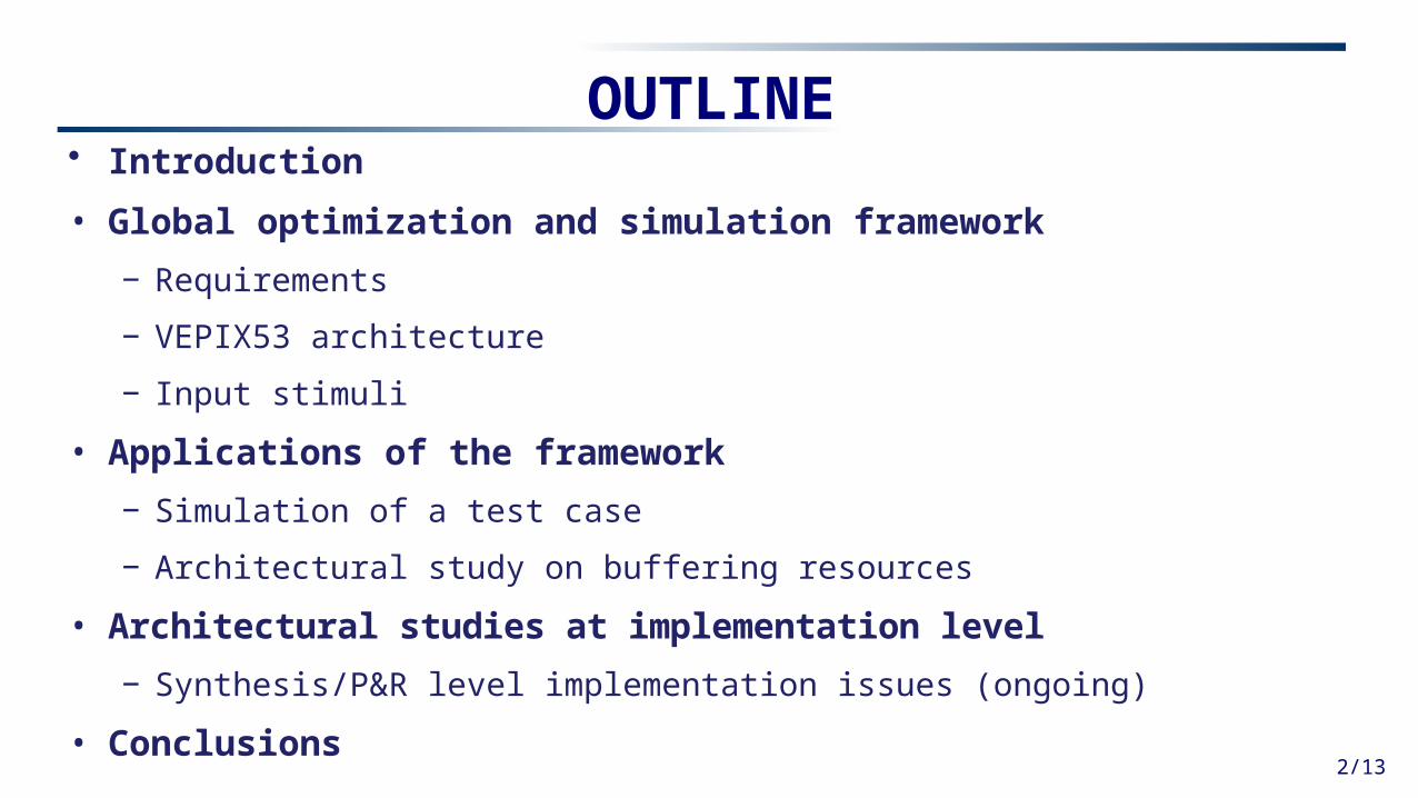
OUTLINE
2/13
• Introduction
• Global optimization and simulation framework
− Requirements
− VEPIX53 architecture
− Input stimuli
• Applications of the framework
− Simulation of a test case
− Architectural study on buffering resources
• Architectural studies at implementation level
− Synthesis/P&R level implementation issues (ongoing)
• Conclusions
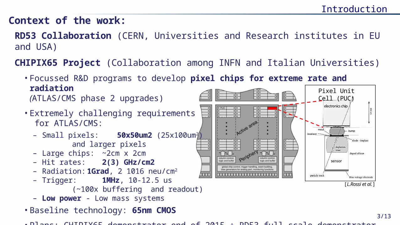
Pixel UnitCell (PUC)
[L.Rossi et al.]
3/13
IntroductionContext of the work:
RD53 Collaboration (CERN, Universities and Research institutes in EU and USA)
CHIPIX65 Project (Collaboration among INFN and Italian Universities)
• Focussed R&D programs to develop pixel chips for extreme rate and radiation(ATLAS/CMS phase 2 upgrades)
• Extremely challenging requirements for ATLAS/CMS:– Small pixels: 50x50um2 (25x100um2)
and larger pixels– Large chips: ~2cm x 2cm – Hit rates: 2(3) GHz/cm2 – Radiation: 1Grad, 2 1016 neu/cm2 – Trigger: 1MHz, 10-12.5 us
(~100x buffering and readout)– Low power - Low mass systems
• Baseline technology: 65nm CMOS
• Plans: CHIPIX65 demonstrator end of 2015 + RD53 full scale demonstrator pixel chip end of 2016
4/13
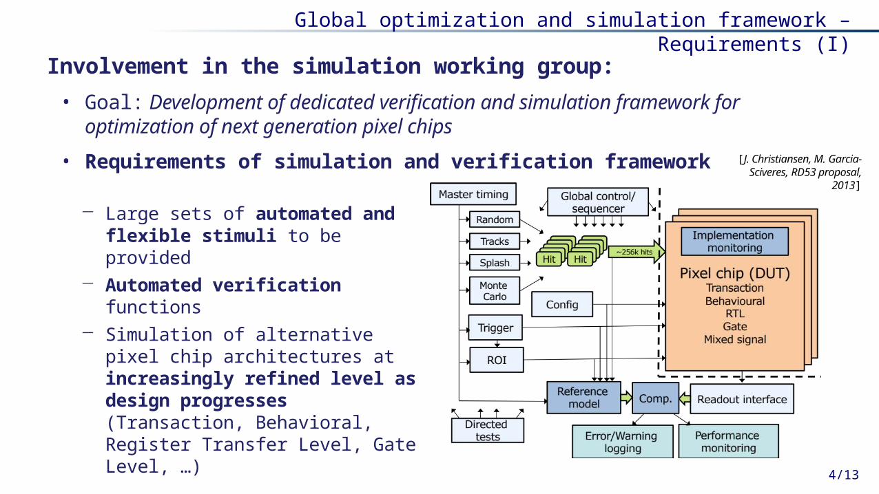
Global optimization and simulation framework – Requirements (I)
Involvement in the simulation working group:
• Goal: Development of dedicated verification and simulation framework for optimization of next generation pixel chips
• Requirements of simulation and verification framework [J. Christiansen, M. Garcia-Sciveres, RD53
proposal, 2013]
− Large sets of automated and flexible stimuli to be provided
− Automated verification functions − Simulation of alternative pixel chip
architectures at increasingly refined level as design progresses (Transaction, Behavioral, Register Transfer Level, Gate Level, …)

5/13
• Framework needed for complex design optimization at all levels of the architecture
• Example: Combined increase in trigger latency and hit rate 100 times higher buffering ∼requirements (strong impact on area and power consumption)– A track crossing the sensor hits a group of pixels
– Efficient processing of hits by grouping pixels in pixel regions (PR) where buffering logic is shared– Different architectures to be evaluated to compare buffering resources needed
interaction point
sensor
Global optimization and simulation framework – Requirements (II)

6/13
TLM port TLM export TLM analysis port/export
TEST SCENARIO
TESTBENCH
TOP MODULE
virtualsequencer
hit UVCtriggerUVC
test library
outputUVC
analysis UVC
reference model
scoreboard
Design Under Test (DUT)
hit_if trigger_if analysis_if output_if
sequencer
driver
subscriber
monitor driver
sequencer
monitorsubscribersmonitor
• Top-module: system (DUT) connected to environment through a set of interfaces
• Testbench: UVM (re-usable) Verification Components (UVCs)
• Test Scenario: defines configuration of verification components and the tests to be run during simulation
Global optimization and simulation framework – VEPIX53 architecture
top UVC
–hit generation and injection–monitoring of pixel chip inputand output
–conformity checks andstatistics collection

7/13
Global optimization and simulation framework – Input stimuli
Different categories of input stimuli:
• Internally generated hits
• External hit patterns
– ROOT format (from CLIC) (N. Alipour Tehrani)
– Text files, ASCII format (from CMS) (E. Migliore, M. Musich, M. Bilal Kiani, A. Tricomi)
– Minimum bias events with variable pixel size, thickness and pileup
– Emulation of digitization + clustering: energy deposit converted in electrons with variable threshold, full scale, electrons/ADC count and digitizer bits
– Non-clusterized data can be requested to CMS; converging to a unique ROOT file format
• Combination of the two

virtualsequencer
hit UVCtrigger UVC
test library
outputUVC
analysis UVC
reference model
scoreboard
ATLAS FEI4 (DUT)
hit_if trigger_if analysis_if
optional
SIG2TLMTLM2SIG SIG2TLMTLM2SIG SIG2TLM
v sequence
output_if
SIG2TLM
top UVC
8/13
Applications of the framework: Simulation of a testcase
Test case for full-chip simulation:
• Design Under Test: ATLAS FEI4 (reference chip) at RTL description level
• Automated verification: (re-)use of reference model and scoreboard
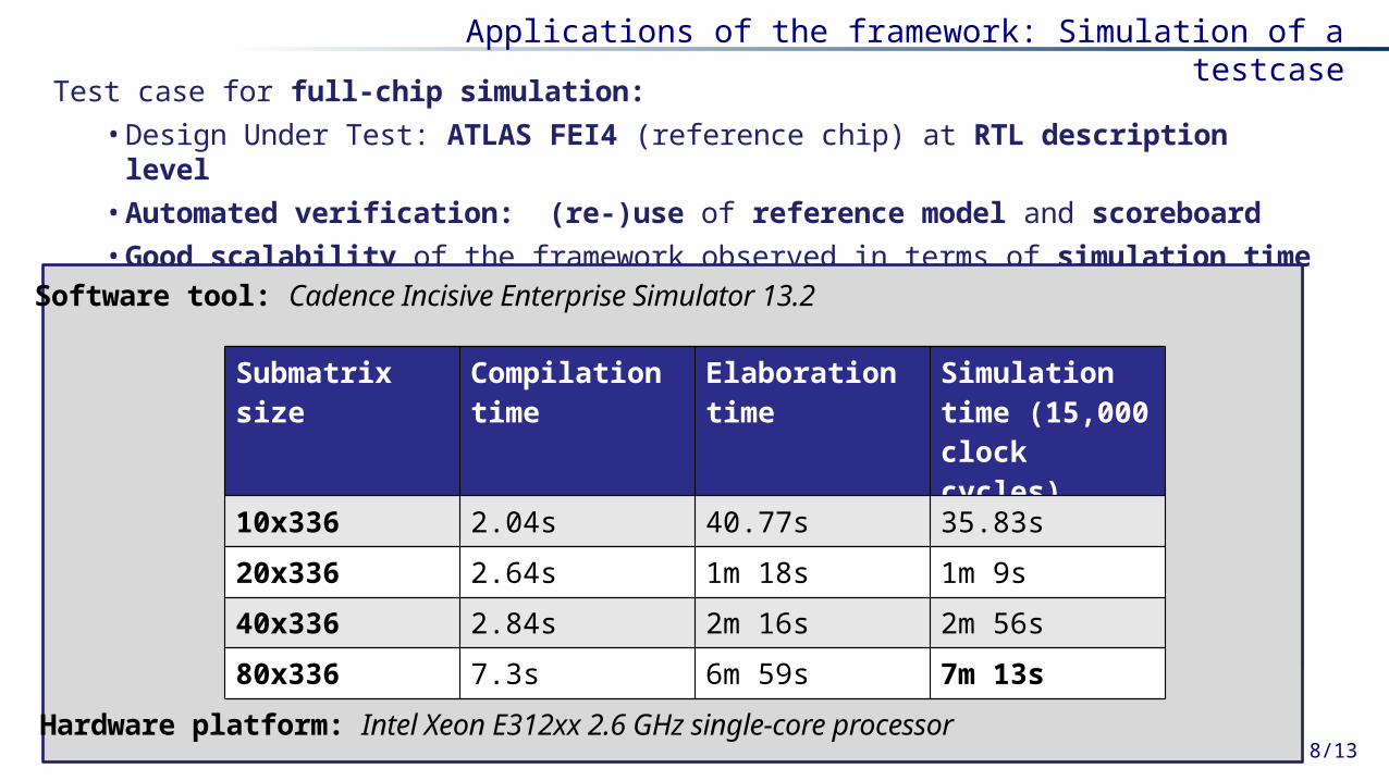
Applications of the framework: Simulation of a testcase
Test case for full-chip simulation:
• Design Under Test: ATLAS FEI4 (reference chip) at RTL description level
• Automated verification: (re-)use of reference model and scoreboard
• Good scalability of the framework observed in terms of simulation time
virtualsequencer
hit UVCtrigger UVC
test library
outputUVC
analysis UVC
reference model
scoreboard
ATLAS FEI4 (DUT)
hit_if trigger_if analysis_if
optional
SIG2TLMTLM2SIG SIG2TLMTLM2SIG SIG2TLM
v sequence
output_if
SIG2TLM
top UVC Submatrix size Compilation time
Elaboration time
Simulation time (15,000 clock cycles)
10x336 2.04s 40.77s 35.83s
20x336 2.64s 1m 18s 1m 9s
40x336 2.84s 2m 16s 2m 56s
80x336 7.3s 6m 59s 7m 13s
8/13
Software tool: Cadence Incisive Enterprise Simulator 13.2
Hardware platform: Intel Xeon E312xx 2.6 GHz single-core processor
9/13
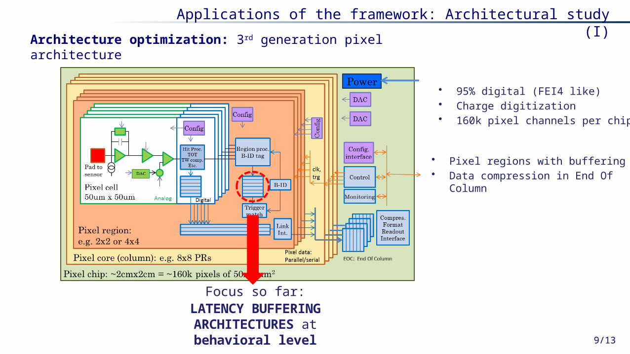
Architecture optimization: 3rd generation pixel architecture
• 95% digital (FEI4 like)• Charge digitization• 160k pixel channels per chip
• Pixel regions with buffering• Data compression in End Of Column
Focus so far:LATENCY BUFFERING ARCHITECTURES at
behavioral level
Applications of the framework: Architectural study (I)
10/13
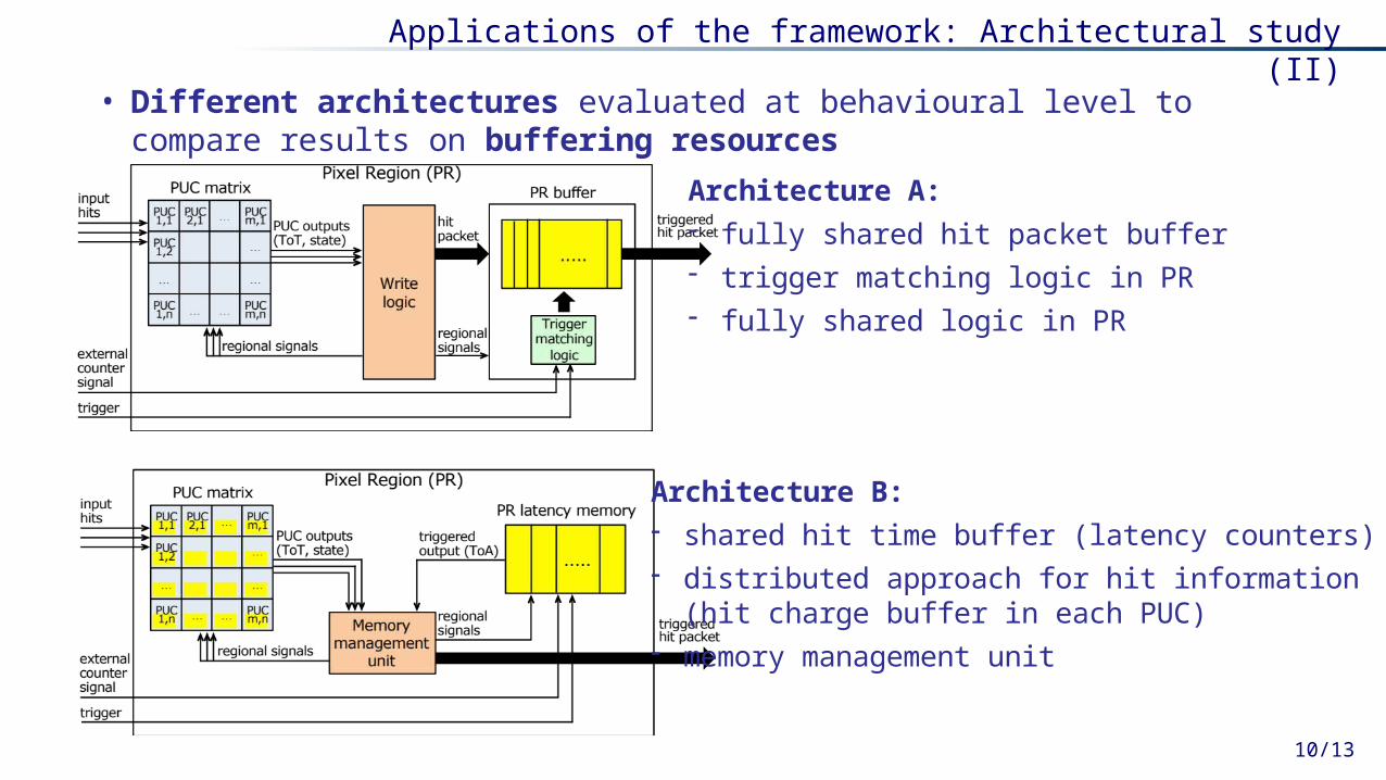
Architecture A: - fully shared hit packet buffer- trigger matching logic in PR- fully shared logic in PR
Applications of the framework: Architectural study (II)
• Different architectures evaluated at behavioural level to compare results on buffering resources
Architecture B: - shared hit time buffer (latency counters)- distributed approach for hit information
(hit charge buffer in each PUC)- memory management unit
11/13
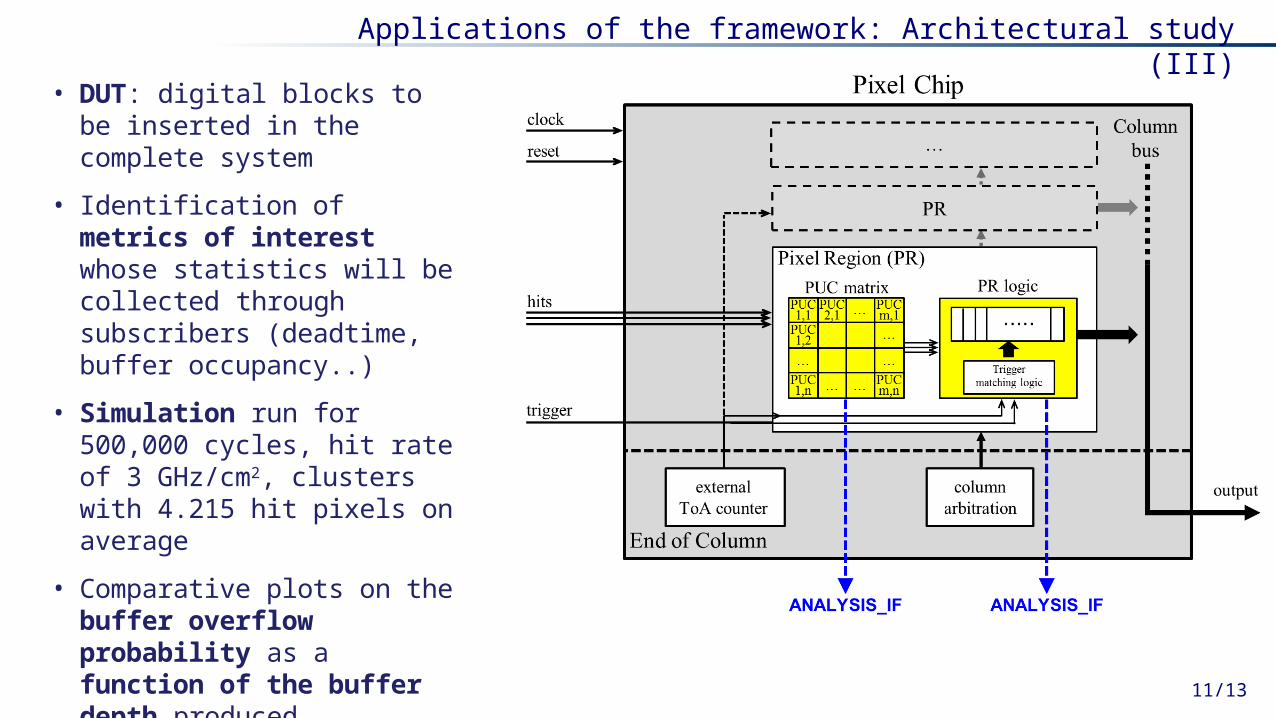
• DUT: digital blocks to be inserted in the complete system
• Identification of metrics of interest whose statistics will be collected through subscribers (deadtime, buffer occupancy..)
• Simulation run for 500,000 cycles, hit rate of 3 GHz/cm2, clusters with 4.215 hit pixels on average
• Comparative plots on the buffer overflow probability as a function of the buffer depth produced
Applications of the framework: Architectural study (III)
12/13
Architectural studies at implementation level
Plans (ongoing/future) :
• Acquire more confidence with RTL compiler and Encounter Digital Implementation tools starting from the pixel region RTL of the FE65P2 prototype
• Evaluate impact of using different buffer size
• Evaluate impact of bigger gate size
• Evaluate impact of clock gating
• Evaluate impact of bigger PR size (i.e. 4x4)
• Evaluate different architectures (possible collaboration with Torino for CHIPIX demonstrator)
• Evaluate impact of using Triple Module Redundancy (TMR)
In parallel evaluate performance in terms of:
• Area
• Power – Average
– Peak: definition/which tools to use under discussion
• SEU Tolerance

CONCLUSIONS
• VEPIX53 versatile simulation and verification environment implemented:– use of UVM standard class library provides re-usability and configurability
– generation of stimuli (internal and imported) and automated verification
– test cases:
• simulation of ATLAS FE-I4
• architectural evaluation on trigger latency buffering logic
• Further developments/ongoing:– further architectural studies on different blocks (e.g. column arbitration, data compression,
…)
– design optimization at implementation level (area, power, radiation tolerance, …)
13/13