inview communication modules - literature library
TRANSCRIPT

Science and Technology ofAdvanced Materials
Plasma-enhanced chemical vapor deposition ofnanocrystalline diamondTo cite this article: Katsuyuki Okada 2007 Sci. Technol. Adv. Mater. 8 624
View the article online for updates and enhancements.
Related contentEffects of Plasma Potential on DiamondDeposition at Low Pressure UsingMagneto-Microwave Plasma ChemicalVapor DepositionJin Wei, Hiroshi Kawarada, Jun-ichi Suzukiet al.
-
Boron-Induced Dramatically EnhancedGrowth of Diamond Grains inNanocrystalline Diamond/HydrogenatedAmorphous Carbon Composite FilmsDeposited by Coaxial Arc PlasmaDepositionYki Katamune, Shinya Ohmagari andTsuyoshi Yoshitake
-
Incubation-Free Growth of PolycrystallineSi Films by Plasma-Enhanced ChemicalVapor Deposition Using Pulsed Dischargeunder Near Atmospheric PressureHirotatsu Kitabatake, Maki Suemitsu,Hiroya Kitahata et al.
-
Recent citationsDebajyoti Das-
Nina Felgen et al-
Zhipeng Wang et al-
This content was downloaded from IP address 95.216.75.56 on 24/11/2018 at 13:56
ARTICLE IN PRESSThe STAM archive is now available from the IOP Publishing website http://www.iop.org/journals/STAM
1468-6996/$ - se
doi:10.1016/j.st
�Tel.: +81 29
E-mail addr
Science and Technology of Advanced Materials 8 (2007) 624–634
www.elsevier.com/locate/stam
Review
Plasma-enhanced chemical vapor depositionof nanocrystalline diamond
Katsuyuki Okada�
National Institute for Materials Science, 1-1 Namiki, Tsukuba, Ibaraki 305-0044, Japan
Received 12 June 2007; received in revised form 8 August 2007; accepted 27 August 2007
Available online 22 October 2007
Abstract
Nanocrystalline diamond films have attracted considerable attention because they have a low coefficient of friction and a low electron
emission threshold voltage. In this paper, the author reviews the plasma-enhanced chemical vapor deposition (PE-CVD) of
nanocrystalline diamond and mainly focuses on the growth of nanocrystalline diamond by low-pressure PE-CVD. Nanocrystalline
diamond particles of 200–700 nm diameter have been prepared in a 13.56MHz low-pressure inductively coupled CH4/CO/H2 plasma.
The bonding state of carbon atoms was investigated by ultraviolet-excited Raman spectroscopy. Electron energy loss spectroscopy
identified sp2-bonded carbons around the 20–50 nm subgrains of nanocrystalline diamond particles. Plasma diagnostics using a
Langmuir probe and the comparison with plasma simulation are also reviewed. The electron energy distribution functions are discussed
by considering different inelastic interaction channels between electrons and heavy particles in a molecular CH4/H2 plasma.
r 2007 NIMS and Elsevier Ltd. All rights reserved.
Keywords: Low-pressure inductively coupled plasma; Nanocrystalline diamond; UV Raman spectroscopy; Resonance Raman scattering; High-resolution
electron energy loss spectroscopy; Electron energy loss spectroscopy; sp2/sp3 chemical mapping; Langmuir probe; Direct simulation Monte Carlo;
Electron energy distribution function
Contents
1. Introduction . . . . . . . . . . . . . . . . . . . . . . . . . . . . . . . . . . . . . . . . . . . . . . . . . . . . . . . . . . . . . . . . . . . . . . . . . . . . . . . 624
2. Growth of nanocrystalline diamond . . . . . . . . . . . . . . . . . . . . . . . . . . . . . . . . . . . . . . . . . . . . . . . . . . . . . . . . . . . . . . 625
2.1. Conventional microwave PE-CVD . . . . . . . . . . . . . . . . . . . . . . . . . . . . . . . . . . . . . . . . . . . . . . . . . . . . . . . . . . . 625
2.2. Low-pressure PE-CVD . . . . . . . . . . . . . . . . . . . . . . . . . . . . . . . . . . . . . . . . . . . . . . . . . . . . . . . . . . . . . . . . . . . 625
3. Spectroscopic characterization . . . . . . . . . . . . . . . . . . . . . . . . . . . . . . . . . . . . . . . . . . . . . . . . . . . . . . . . . . . . . . . . . . 626
3.1. SEM . . . . . . . . . . . . . . . . . . . . . . . . . . . . . . . . . . . . . . . . . . . . . . . . . . . . . . . . . . . . . . . . . . . . . . . . . . . . . . . . 626
3.2. Raman spectroscopy . . . . . . . . . . . . . . . . . . . . . . . . . . . . . . . . . . . . . . . . . . . . . . . . . . . . . . . . . . . . . . . . . . . . . 627
3.3. HREELS . . . . . . . . . . . . . . . . . . . . . . . . . . . . . . . . . . . . . . . . . . . . . . . . . . . . . . . . . . . . . . . . . . . . . . . . . . . . . 629
3.4. EELS mapping . . . . . . . . . . . . . . . . . . . . . . . . . . . . . . . . . . . . . . . . . . . . . . . . . . . . . . . . . . . . . . . . . . . . . . . . . 630
4. Plasma diagnostics and simulation . . . . . . . . . . . . . . . . . . . . . . . . . . . . . . . . . . . . . . . . . . . . . . . . . . . . . . . . . . . . . . . 632
Acknowledgments . . . . . . . . . . . . . . . . . . . . . . . . . . . . . . . . . . . . . . . . . . . . . . . . . . . . . . . . . . . . . . . . . . . . . . . . . . . 633
References . . . . . . . . . . . . . . . . . . . . . . . . . . . . . . . . . . . . . . . . . . . . . . . . . . . . . . . . . . . . . . . . . . . . . . . . . . . . . . . . 633
e front matter r 2007 NIMS and Elsevier Ltd. All rights rese
am.2007.08.008
860 4322; fax: +81 29 852 7449.
ess: [email protected]
1. Introduction
Covalently bonded disordered thin-film materials havebeen of considerable interest from both fundamental and
rved.

ARTICLE IN PRESSK. Okada / Science and Technology of Advanced Materials 8 (2007) 624–634 625
applied perspectives in the last 20 years since the chemicalvapor deposition (CVD) of diamond was developed,followed by that of fullerenes and carbon nanotubes [1,2].Among them, amorphous and nanostructured carbon filmsare currently being extensively studied for use as electronemitters, cold-cathode sources, and hard low-frictioncoatings. From the fundamental perspective, on the otherhand, the structure of these materials contains boththreefold-coordinated (sp2-bonded) and fourfold-coordi-nated (sp3-bonded) carbon atoms. Nanocrystalline dia-mond films have also attracted attention [3] because theyhave a low coefficient of friction and a low electronemission threshold voltage. The small grain size (approxi-mately 5–100 nm) gives films valuable tribological andfield-emission properties comparable to those of conven-tional polycrystalline diamond films. Furthermore, appli-cations for micro-electro-mechanical systems (MEMS)devices, metal-semiconductor field effect transistors (MES-FETs), electrochemical electrodes, and biochemical devicesthat take advantage of these excellent properties have beenproposed [4–6].
Recent dry plasma processes (e.g., deposition, coating,etching) require a wide area and high-density plasma at lowpressures (o1Torr) [7]. An electron cyclotron resonance(ECR) plasma was first developed to satisfy these condi-tions. Subsequently, a helicon-wave-excited plasma wasemployed. It was found [8] that the density of aninductively coupled plasma (ICP) becomes high at lowpressures. Amorim et al. [9] reported that the plasmadensity of ICP after the transition from a low-densityE-discharge to a high-density H-discharge reaches1012 cm�3. It is necessary in plasma-enhanced chemicalvapor deposition (PE-CVD) to obtain sufficient radical fluxfor deposition. Thus, ICP is thought to be promising foruse in PE-CVD at low pressures.
In this review article, the author’s own studies on thesynthesis of nanocrystalline diamond by low-pressure ICP-CVD and its spectroscopic characterization are mainlydescribed. Plasma diagnostics using a Langmuir probe andthe comparison with plasma simulation are also reviewed.
2. Growth of nanocrystalline diamond
2.1. Conventional microwave PE-CVD
A microwave plasma is most commonly used for the PE-CVD of diamond films [10], in which the conventionalpressure of deposition is approximately 20–50Torr. ACH4/H2 mixture, in which the CH4 content ([CH4]) isusually less than 5%, leads to mm-size polycrystallinediamond films. One method of synthesizing nanocrystallinediamond films is to increase [CH4] to up to 10% while thesubstrate temperature is kept constant [11–13]. Theresultant morphology changes from faceted microcrystalsto spherical nanocrystals.
Another method is to substitute a noble gas forhydrogen while [CH4] is kept constant. Gruen and co-
workers [14,15] demonstrated the synthesis of nanocrystal-line diamond films in a CH4/Ar or C60/Ar microwavedischarge, without the addition of hydrogen. Extensivecharacterization by X-ray diffraction (XRD) analysis,transmission electron microscopy (TEM), and electronenergy loss spectroscopy (EELS) showed [16] that the filmsconsisted of a pure crystalline diamond phase with grainsize ranging from 3 to 20 nm. They also proposed fromplasma diagnostics [17] and theoretical calculations [18]that C2 dimers may be responsible for the growth of thevery fine-grained diamond films, whereas CH3 radicals aregenerally believed to be a precursor for the diamondgrowth.Recently, Philip et al. [4] reported the deposition of
nanocrystalline diamond films under the conventionaldeposition conditions for mm-size polycrystalline diamondfilms. The substrate pretreatment by the deposition of athin H-terminated a-C film followed by the seeding ofnanodiamond powder increased the nucleation density onthe Si substrate to over 1012/cm2. The resultant films weregrown to thicknesses ranging from 100 nm to 5 mm, and thethermal conductivity ranged from 2.5 to 12W/cmK.In addition to microwave plasma, direct current (dc)
[19], hot filament [20], magnetron sputtering [21], and radiofrequency (rf) plasmas [22–24] have been utilized fornanocrystalline diamond deposition. Amaratunga et al.[23,24], using CH4/Ar rf plasma, reported that single-crystal diffraction patterns obtained from nanocrystallinediamond grains all show {1 1 1} twinning.The stability of nanocrystalline diamond has been
discussed from the theoretical point of view by severalauthors. Badziag et al. [25] pointed out, from the results ofsemiempirical quantum chemistry calculations, that suffi-ciently small nanocrystalline diamond (3–5 nm in diameter)may be more stable than graphite due to the formation ofC–H bonds at the growing surface. Barnard et al. [26]performed ab initio calculations on nanocrystalline dia-mond of up to approximately 1 nm in diameter. The resultsrevealed that the surfaces of cubic crystals exhibitreconstruction and relaxation comparable to that of bulkdiamond, while the surfaces of octahedral and cubo-octahedral crystals show a transition from sp3 to sp2
bonding.
2.2. Low-pressure PE-CVD
While a microwave plasma is most commonly used forthe PE-CVD of diamond films, ECR plasma is the onlyplasma used for diamond deposition at pressures below1Torr [27–29]. Bozeman et al. [30] reported diamonddeposition at 4Torr using a planar ICP, and there are a fewreports that describe the synthesis of diamond by low-pressure ICP. Okada and co-workers [31–33] first reportedthe synthesis of nanocrystalline diamond particles in a low-pressure CH4/CO/H2 ICP, followed by Teii and Yoshida[34] using the same gas-phase chemistry.
ARTICLE IN PRESS
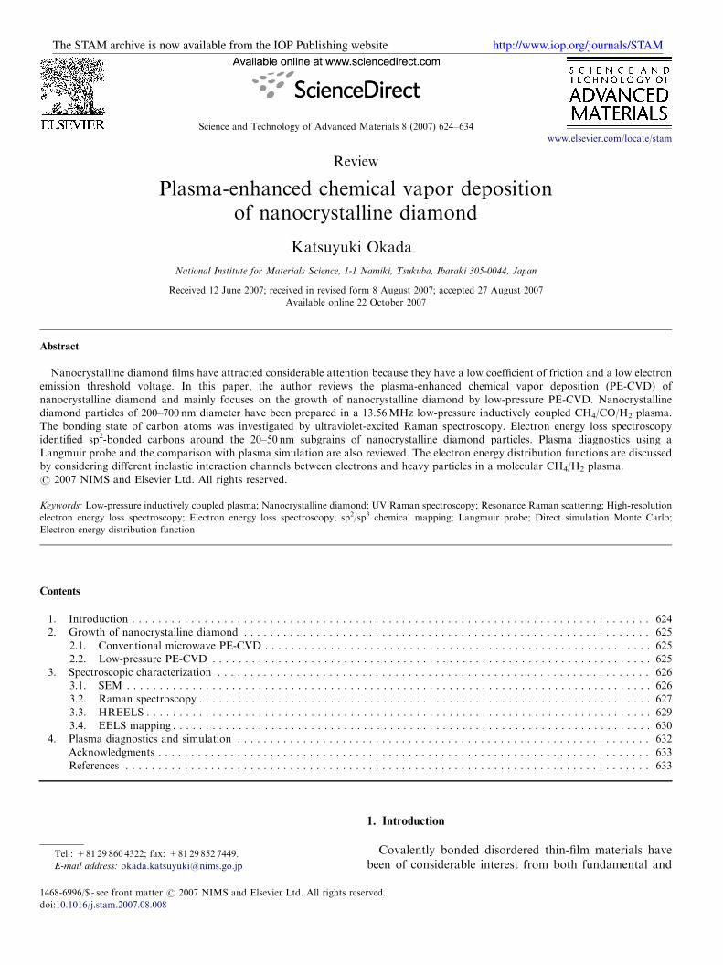
Fig. 1. Schematic description of low-pressure inductively coupled rf
plasma CVD system.
K. Okada / Science and Technology of Advanced Materials 8 (2007) 624–634626
In the PE-CVD of diamond films, oxygen is added to aCH4/H2 system to obtain a high growth rate and/or animprovement of the quality of the resultant films [35–38].Several authors have discussed the role of oxygen indiamond growth. Mucha et al. [37] pointed out thatthe addition of oxygen to a CH4/H2 system increases theconcentration of atomic hydrogen; correspondingly, theformation of amorphous and graphitic carbon, whichwould otherwise inhibit diamond growth, is suppressed.From a detailed chemical kinetics model that describesboth gas phase and surface processes occurring in diamondCVD, Frenklach and Wang [38] postulated that OHradicals and atomic oxygen gasify sp2 carbon and suppressthe formation of aromatic species in the gas phase. Teii andco-workers [39,40] pointed out that the OH radicalsresulting predominantly from loss reactions between by-product O atoms and H2 and CH4 molecules stronglyenhance diamond growth.
A 13.56MHz low-pressure ICP system [31–33] has beenutilized as a source of radicals for PE-CVD and applied toprepare diamond films from a CH4/H2 plasma. CO wasadded to a CH4/H2 plasma to clarify the effect of oxygen-containing radicals on diamond growth. A schematic viewof the apparatus is shown in Fig. 1. It consists of a water-cooled quartz tube surrounded by a Teflon tube and astainless-steel growth chamber. An ICP was generated byapplying a 13.56MHz rf power of 1 kW to a three-turnhelical coil wound around the Teflon tube. The chamberwas pre-evacuated to 5� 10�5 Torr using a turbomolecularpump (200 l/s). The electrostatic (capacitive) coupling fromthe rf coil to the plasma in a low-pressure ICP causescontamination due to the etching of the quartz tube. Toreduce the electrostatic coupling, a Faraday shield wasinserted between the rf coil and the quartz tube.A grounded copper plate with slits at regular intervalsalong the azimuthal direction was wrapped around thequartz tube. A substrate holder was manipulated from thetop of the chamber. Molybdenum plates and silicon (1 0 0)wafers (f 10mm) were used as the substrate. The substratewas heated using a tungsten filament. The substratetemperature (Ts) was monitored using a sheathed thermo-couple and maintained at a prescribed temperature within71 1C using a proportional integral derivative (PID)controller. The deposition conditions were as follows.The flow rates of CH4 and H2 were maintained at 4.5 and75 sccm, respectively, whereas the flow rate of CO ([CO])was 0, 1.0, or 10 sccm. The total gas pressure (Pr) wasvaried from 45 to 50mTorr. Ts was maintained at 900 1C.The deposition duration was 2 h.
3. Spectroscopic characterization
3.1. SEM
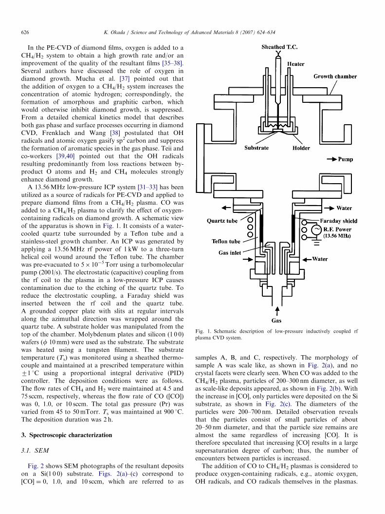
Fig. 2 shows SEM photographs of the resultant depositson a Si(1 0 0) substrate. Figs. 2(a)–(c) correspond to[CO] ¼ 0, 1.0, and 10 sccm, which are referred to as
samples A, B, and C, respectively. The morphology ofsample A was scale like, as shown in Fig. 2(a), and nocrystal facets were clearly seen. When CO was added to theCH4/H2 plasma, particles of 200–300 nm diameter, as wellas scale-like deposits appeared, as shown in Fig. 2(b). Withthe increase in [CO], only particles were deposited on the Sisubstrate, as shown in Fig. 2(c). The diameters of theparticles were 200–700 nm. Detailed observation revealsthat the particles consist of small particles of about20–50 nm diameter, and that the particle size remains arealmost the same regardless of increasing [CO]. It istherefore speculated that increasing [CO] results in a largesupersaturation degree of carbon; thus, the number ofencounters between particles is increased.The addition of CO to CH4/H2 plasmas is considered to
produce oxygen-containing radicals, e.g., atomic oxygen,OH radicals, and CO radicals themselves in the plasmas.
ARTICLE IN PRESS
Fig. 2. SEM micrographs of obtained deposits: (a) [CH4]/[CO] ¼ 4.5/0 sccm, (b) [CH4]/[CO] ¼ 4.5/1.0 sccm, and (c) [CH4]/[CO] ¼ 4.5/10 sccm.
K. Okada / Science and Technology of Advanced Materials 8 (2007) 624–634 627
As mentioned above, a morphological change from a scale-like deposit to the deposition of particles took place uponadding CO. Also, the number of encounters betweenparticles increased with an increase in [CO]. According tothe TEM and XRD patterns [33], nondiamond carbon waseffectively removed with an increase in [CO]. We thereforepresume that oxygen-containing radicals produced by theaddition of CO play an effective role in the removal ofnondiamond carbon under diamond growth conditionsand that the CO additive results in a large supersaturationdegree of carbon. This is consistent with the previouslyreported hypotheses [37,38] that OH radicals and atomicoxygen gasify sp2 carbon and that they suppress theformation of amorphous carbon and graphitic carbon.
3.2. Raman spectroscopy
Raman spectroscopy is a nondestructive method ofstudying the vibrational band structure of materials. It hasbeen extensively used for the characterization of diamond[41–44], graphite [45], and diamond-like carbon (DLC)[42,43,46–49]. Raman scattering is the most populartechnique for identifying sp3 bonding in diamond and sp2
bonding in graphite and DLC. Although Raman scatteringshould represent the phonon density of states (PDOS)weighted by a coupling parameter, Raman spectroscopy ofsp2-bonded carbon with an excitation wavelength in thevisible range (514, 488 nm, etc.) does not provide a goodrepresentation of the PDOS [50]. Since the local sp2-bonded carbon energy gap of �2 eV is comparable to theenergy of visible Raman excitation, the sp2-bonded carbonnetwork exhibits electronic p–p* transition resonanceenhancement in the Raman cross-section [43,48–50]. On
the other hand, sp3-bonded carbon does not exhibit such aresonance effect because of the higher local gap of �5.5 eV.As a result, the Raman spectra obtained using visibleexcitation are completely dominated by sp2-bonded car-bon. However, Raman spectroscopy with ultraviolet (UV)excitation has recently been used for characterizing DLC[50–53]. The advantage of UV Raman spectroscopy is thatit eliminates the resonance effect of sp2-bonded carbon.Excitation of 244 nm (5.1 eV) is far from the energy of thepreviously mentioned sp2-bonded carbon resonance. It isthus expected that the resonance Raman scattering fromsp2-bonded carbon is suppressed and that the signal fromsp3-bonded carbon may be increased. UV Raman spectraof tetrahedral amorphous carbon (t-aC) films containingsp3 bonding predominantly exhibit a peak at �1150 cm�1
attributed to an sp3-bonded carbon network [50–52].Okada et al. [54] first applied UV Raman spectroscopy tothe characterization of the bonding structures of nano-crystalline diamond. Sun et al. [55] reported the UVRaman characteristics of nanocrystalline diamond films forgrain sizes 120–28 nm. They pointed out that the downshiftand broadening of the diamond peak with decreasing grainsize are consistent with the phonon confinement model. Onthe other hand, Prawer et al. [56] reported the visibleRaman spectra for nanocrystalline diamond powder withgrains of �5 nm diameter. The peaks at 500, 1140, 1132,and 1630 cm�1 are compared with the calculated vibra-tional density of states (VDOS) of diamond, and the originof features in the vibrational spectrum obtained fromnanocrystalline diamond has been hypothesized.In Raman measurements [57], the 514 nm line of an Ar+
laser, the 325 nm line of a He–Cd laser, and the 244 nm lineof an intracavity frequency-doubled Ar+ laser were

ARTICLE IN PRESS
1000 1200 1400 1600 1800
Raman shift (cm-1)
Inte
nsity
(ar
b. u
nits
)
CH4/CO=4.5/10
CH4/CO=4.5/1
CH4/CO=4.5/0
Fig. 3. The 514-nm-excited Raman spectra of obtained deposits for
different gas mixtures: (a) [CH4]/[CO] ¼ 4.5/0 sccm, (b) [CH4]/[CO] ¼
4.5/1.0 sccm, and (c) [CH4]/[CO] ¼ 4.5/10 sccm.
K. Okada / Science and Technology of Advanced Materials 8 (2007) 624–634628
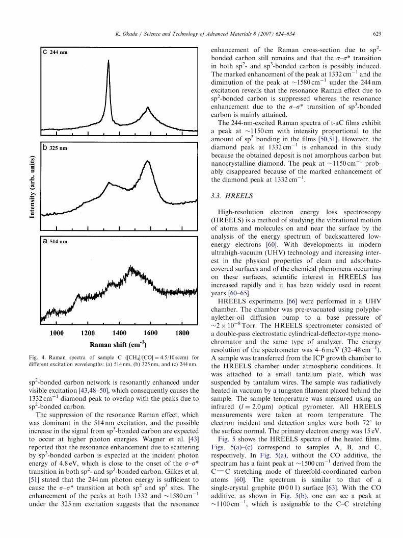
employed. The incident laser beam was directed onto thesample surface under a backscattering geometry at roomtemperature. For the 514 nm excitation, the scattered lightwas collected and dispersed in a SPEX 1403 doublemonochromator and detected using a photomultiplier.The laser output power was 300mW. For the 325 and244 nm excitation, the scattered light was collected usingfused-silica optics and analyzed using a UV-enhancedCCD camera with a Renishaw micro-Raman System 1000spectrometer modified for use at 325 and 244 nm,respectively. A laser output of 10mW was used, whichresulted in an incident power at the sample of approxi-mately 1.5mW. The spectral resolution was approximately2 cm�1. It was verified that no photoalteration of thesamples occurred during the UV laser irradiation byconfirming that the visible Raman spectra were unalteredafter the UV Raman measurements.
Fig. 3 shows the 514-nm-excited Raman spectra.Figs. 3(a)–(c) correspond to samples A, B, and C,respectively. The Raman spectrum of sample A exhibitstwo peaks at �1355 cm�1 (D peak) and �1580 cm�1
(G peak) assigned to sp2 bonding [45]. New peaks appearat �1150 and �1480 cm�1 in sample B. The former peak isdue to sp3 bonding. Nemanich and co-workers [42,44]assigned the peak at �1150 cm�1 to microcrystalline oramorphous diamond. Prawer and Nugent [58] attributedthe peak at 1100–1150 cm�1 to the surface phonon mode ofdiamond from EELS studies of nanophase diamondpowder. On the other hand, Ferrari and Robertson [59]have recently proposed another interpretation, that thepeak at �1150 cm�1 is not attributed to nanocrystallinediamond but to the sp2 bonding of a trans-polyacetyleneoligomer of a given conjugation length. The peak at�1480 cm�1 is probably related to amorphous sp2 struc-tures [44], although it is downshifted from the G peak. BothD and G peaks become relatively small compared withthose of sample A. The peak at �950 cm�1 is derived fromscattering by two transverse-optical (TO) phonons of thesilicon substrate [43]. The incident laser beam reached thesubstrate because the substrate was not fully covered by thedeposit, as shown in Fig. 2(b). In the Raman spectrum ofsample C, the G peak becomes a shoulder and the D peakbecomes faint, while the peak at �1480 cm�1 has thehighest intensity and the peak at �1150 cm�1 still remains.However, the three spectra in Fig. 3 do not clearly exhibitthe 1332 cm�1 diamond peak. These features of the Ramanspectra imply that the deposit due to CH4/H2 predomi-nantly contains sp2 bonding; the addition of CO to CH4/H2
produces a mixture of sp2 and sp3 bonding; an increase in[CO] brings about an increase in sp3 bonding. These trendsare consistent with the TEM and XRD observations, whichreveal that the increase in [CO] improves the crystallinity ofthe deposit.
Fig. 4 shows a sequence of Raman spectra from sampleC for different excitation wavelengths. Figs. 4(a)–(c)correspond to 514, 325, and 244 nm, respectively. Incontrast with the spectrum obtained from 514 nm excita-
tion, the 325-nm-excited Raman spectrum exhibits a clearpeak at 1332 cm�1 and a marked enhancement of the peakat �1580 cm�1, while the peak at �1150 cm�1 becomes ashoulder. In the 244-nm-excited Raman spectrum, only thepeak at 1332 cm�1 is enhanced, whereas the peak at�1580 cm�1 is weakened. Neither peak nor shoulder canbe recognized at �1150 cm�1. The Raman spectrum inFig. 4(a) is superimposed on a broad photoluminescencebackground. This background diminishes with increasingexcitation photon energy as shown in Figs. 4(b) and (c).The TEM and XRD patterns revealed [33] that the
deposit is not amorphous carbon but nanocrystallinediamond. Nonetheless, the 514-nm-excited Raman spectrado not exhibit a clear diamond peak at 1332 cm�1,although the peak due to the sp3-bonded carbon networkappears at �1150 cm�1. The Raman cross-section of the
ARTICLE IN PRESS
Fig. 4. Raman spectra of sample C ([CH4]/[CO] ¼ 4.5/10 sccm) for
different excitation wavelengths: (a) 514 nm, (b) 325 nm, and (c) 244 nm.
K. Okada / Science and Technology of Advanced Materials 8 (2007) 624–634 629
sp2-bonded carbon network is resonantly enhanced undervisible excitation [43,48–50], which consequently causes the1332 cm�1 diamond peak to overlap with the peaks due tosp2-bonded carbon.
The suppression of the resonance Raman effect, whichwas dominant in the 514 nm excitation, and the possibleincrease in the signal from sp3-bonded carbon are expectedto occur at higher photon energies. Wagner et al. [43]reported that the resonance enhancement due to scatteringby sp3-bonded carbon is expected at the incident photonenergy of 4.8 eV, which is close to the onset of the s–s*transition in both sp2- and sp3-bonded carbon. Gilkes et al.[51] stated that the 244 nm photon energy is sufficient tocause the s–s* transition at both sp2 and sp3 sites. Theenhancement of the peaks at both 1332 and �1580 cm�1
under the 325 nm excitation suggests that the resonance
enhancement of the Raman cross-section due to sp2-bonded carbon still remains and that the s–s* transitionin both sp2- and sp3-bonded carbon is possibly induced.The marked enhancement of the peak at 1332 cm�1 and thediminution of the peak at �1580 cm�1 under the 244 nmexcitation reveals that the resonance Raman effect due tosp2-bonded carbon is suppressed whereas the resonanceenhancement due to the s–s* transition of sp3-bondedcarbon is mainly attained.The 244-nm-excited Raman spectra of t-aC films exhibit
a peak at �1150 cm with intensity proportional to theamount of sp3 bonding in the films [50,51]. However, thediamond peak at 1332 cm�1 is enhanced in this studybecause the obtained deposit is not amorphous carbon butnanocrystalline diamond. The peak at �1150 cm�1 prob-ably disappeared because of the marked enhancement ofthe diamond peak at 1332 cm�1.
3.3. HREELS
High-resolution electron energy loss spectroscopy(HREELS) is a method of studying the vibrational motionof atoms and molecules on and near the surface by theanalysis of the energy spectrum of backscattered low-energy electrons [60]. With developments in modernultrahigh-vacuum (UHV) technology and increasing inter-est in the physical properties of clean and adsorbate-covered surfaces and of the chemical phenomena occurringon these surfaces, scientific interest in HREELS hasincreased rapidly and it has been widely used in recentyears [60–65].HREELS experiments [66] were performed in a UHV
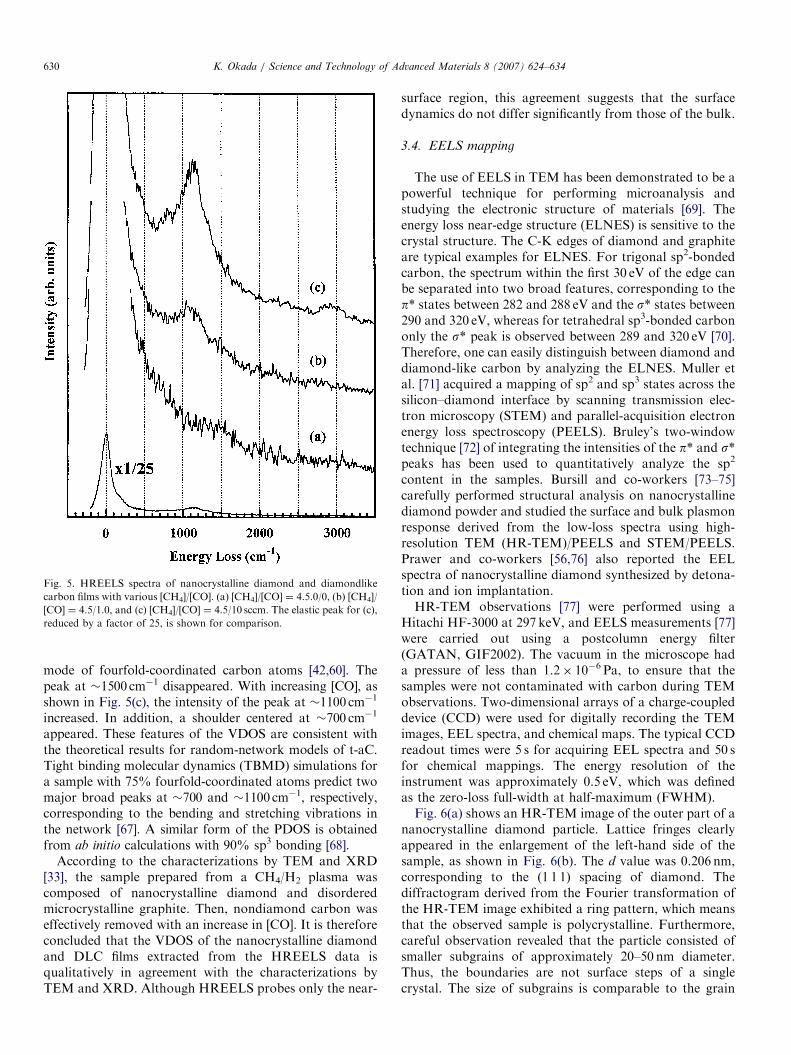
chamber. The chamber was pre-evacuated using polyphe-nylether-oil diffusion pump to a base pressure of�2� 10�8 Torr. The HREELS spectrometer consisted ofa double-pass electrostatic cylindrical-deflector-type mono-chromator and the same type of analyzer. The energyresolution of the spectrometer was 4–6meV (32–48 cm�1).A sample was transferred from the ICP growth chamber tothe HREELS chamber under atmospheric conditions. Itwas attached to a small tantalum plate, which wassuspended by tantalum wires. The sample was radiativelyheated in vacuum by a tungsten filament placed behind thesample. The sample temperature was measured using aninfrared (l ¼ 2.0 mm) optical pyrometer. All HREELSmeasurements were taken at room temperature. Theelectron incident and detection angles were both 721 tothe surface normal. The primary electron energy was 15 eV.Fig. 5 shows the HREELS spectra of the heated films.
Figs. 5(a)–(c) correspond to samples A, B, and C,respectively. In Fig. 5(a), without the CO additive, thespectrum has a faint peak at �1500 cm�1 derived from theCQC stretching mode of threefold-coordinated carbonatoms [60]. The spectrum is similar to that of asingle-crystal graphite (0 0 0 1) surface [63]. With the COadditive, as shown in Fig. 5(b), one can see a peak at�1100 cm�1, which is assignable to the C–C stretching
ARTICLE IN PRESS
Fig. 5. HREELS spectra of nanocrystalline diamond and diamondlike
carbon films with various [CH4]/[CO]. (a) [CH4]/[CO] ¼ 4.5.0/0, (b) [CH4]/
[CO] ¼ 4.5/1.0, and (c) [CH4]/[CO] ¼ 4.5/10 sccm. The elastic peak for (c),
reduced by a factor of 25, is shown for comparison.
K. Okada / Science and Technology of Advanced Materials 8 (2007) 624–634630
mode of fourfold-coordinated carbon atoms [42,60]. Thepeak at �1500 cm�1 disappeared. With increasing [CO], asshown in Fig. 5(c), the intensity of the peak at �1100 cm�1
increased. In addition, a shoulder centered at �700 cm�1
appeared. These features of the VDOS are consistent withthe theoretical results for random-network models of t-aC.Tight binding molecular dynamics (TBMD) simulations fora sample with 75% fourfold-coordinated atoms predict twomajor broad peaks at �700 and �1100 cm�1, respectively,corresponding to the bending and stretching vibrations inthe network [67]. A similar form of the PDOS is obtainedfrom ab initio calculations with 90% sp3 bonding [68].
According to the characterizations by TEM and XRD[33], the sample prepared from a CH4/H2 plasma wascomposed of nanocrystalline diamond and disorderedmicrocrystalline graphite. Then, nondiamond carbon waseffectively removed with an increase in [CO]. It is thereforeconcluded that the VDOS of the nanocrystalline diamondand DLC films extracted from the HREELS data isqualitatively in agreement with the characterizations byTEM and XRD. Although HREELS probes only the near-
surface region, this agreement suggests that the surfacedynamics do not differ significantly from those of the bulk.
3.4. EELS mapping
The use of EELS in TEM has been demonstrated to be apowerful technique for performing microanalysis andstudying the electronic structure of materials [69]. Theenergy loss near-edge structure (ELNES) is sensitive to thecrystal structure. The C-K edges of diamond and graphiteare typical examples for ELNES. For trigonal sp2-bondedcarbon, the spectrum within the first 30 eV of the edge canbe separated into two broad features, corresponding to thep* states between 282 and 288 eV and the s* states between290 and 320 eV, whereas for tetrahedral sp3-bonded carbononly the s* peak is observed between 289 and 320 eV [70].Therefore, one can easily distinguish between diamond anddiamond-like carbon by analyzing the ELNES. Muller etal. [71] acquired a mapping of sp2 and sp3 states across thesilicon–diamond interface by scanning transmission elec-tron microscopy (STEM) and parallel-acquisition electronenergy loss spectroscopy (PEELS). Bruley’s two-windowtechnique [72] of integrating the intensities of the p* and s*peaks has been used to quantitatively analyze the sp2
content in the samples. Bursill and co-workers [73–75]carefully performed structural analysis on nanocrystallinediamond powder and studied the surface and bulk plasmonresponse derived from the low-loss spectra using high-resolution TEM (HR-TEM)/PEELS and STEM/PEELS.Prawer and co-workers [56,76] also reported the EELspectra of nanocrystalline diamond synthesized by detona-tion and ion implantation.HR-TEM observations [77] were performed using a
Hitachi HF-3000 at 297 keV, and EELS measurements [77]were carried out using a postcolumn energy filter(GATAN, GIF2002). The vacuum in the microscope hada pressure of less than 1.2� 10�6 Pa, to ensure that thesamples were not contaminated with carbon during TEMobservations. Two-dimensional arrays of a charge-coupleddevice (CCD) were used for digitally recording the TEMimages, EEL spectra, and chemical maps. The typical CCDreadout times were 5 s for acquiring EEL spectra and 50 sfor chemical mappings. The energy resolution of theinstrument was approximately 0.5 eV, which was definedas the zero-loss full-width at half-maximum (FWHM).Fig. 6(a) shows an HR-TEM image of the outer part of a
nanocrystalline diamond particle. Lattice fringes clearlyappeared in the enlargement of the left-hand side of thesample, as shown in Fig. 6(b). The d value was 0.206 nm,corresponding to the (1 1 1) spacing of diamond. Thediffractogram derived from the Fourier transformation ofthe HR-TEM image exhibited a ring pattern, which meansthat the observed sample is polycrystalline. Furthermore,careful observation revealed that the particle consisted ofsmaller subgrains of approximately 20–50 nm diameter.Thus, the boundaries are not surface steps of a singlecrystal. The size of subgrains is comparable to the grain
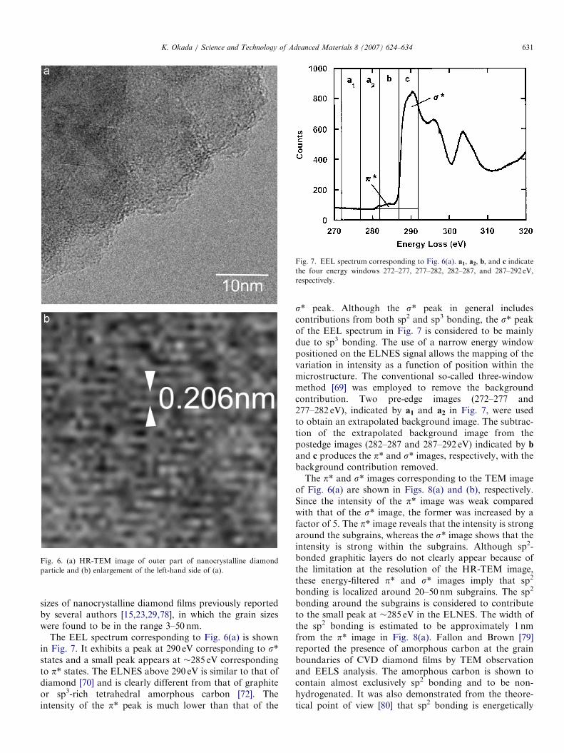
ARTICLE IN PRESS
Fig. 6. (a) HR-TEM image of outer part of nanocrystalline diamond
particle and (b) enlargement of the left-hand side of (a).
Fig. 7. EEL spectrum corresponding to Fig. 6(a). a1, a2, b, and c indicate
the four energy windows 272–277, 277–282, 282–287, and 287–292 eV,
respectively.
K. Okada / Science and Technology of Advanced Materials 8 (2007) 624–634 631
sizes of nanocrystalline diamond films previously reportedby several authors [15,23,29,78], in which the grain sizeswere found to be in the range 3–50 nm.
The EEL spectrum corresponding to Fig. 6(a) is shownin Fig. 7. It exhibits a peak at 290 eV corresponding to s*states and a small peak appears at �285 eV correspondingto p* states. The ELNES above 290 eV is similar to that ofdiamond [70] and is clearly different from that of graphiteor sp3-rich tetrahedral amorphous carbon [72]. Theintensity of the p* peak is much lower than that of the
s* peak. Although the s* peak in general includescontributions from both sp2 and sp3 bonding, the s* peakof the EEL spectrum in Fig. 7 is considered to be mainlydue to sp3 bonding. The use of a narrow energy windowpositioned on the ELNES signal allows the mapping of thevariation in intensity as a function of position within themicrostructure. The conventional so-called three-windowmethod [69] was employed to remove the backgroundcontribution. Two pre-edge images (272–277 and277–282 eV), indicated by a1 and a2 in Fig. 7, were usedto obtain an extrapolated background image. The subtrac-tion of the extrapolated background image from thepostedge images (282–287 and 287–292 eV) indicated by b
and c produces the p* and s* images, respectively, with thebackground contribution removed.The p* and s* images corresponding to the TEM image
of Fig. 6(a) are shown in Figs. 8(a) and (b), respectively.Since the intensity of the p* image was weak comparedwith that of the s* image, the former was increased by afactor of 5. The p* image reveals that the intensity is strongaround the subgrains, whereas the s* image shows that theintensity is strong within the subgrains. Although sp2-bonded graphitic layers do not clearly appear because ofthe limitation at the resolution of the HR-TEM image,these energy-filtered p* and s* images imply that sp2
bonding is localized around 20–50 nm subgrains. The sp2
bonding around the subgrains is considered to contributeto the small peak at �285 eV in the ELNES. The width ofthe sp2 bonding is estimated to be approximately 1 nmfrom the p* image in Fig. 8(a). Fallon and Brown [79]reported the presence of amorphous carbon at the grainboundaries of CVD diamond films by TEM observationand EELS analysis. The amorphous carbon is shown tocontain almost exclusively sp2 bonding and to be non-hydrogenated. It was also demonstrated from the theore-tical point of view [80] that sp2 bonding is energetically

ARTICLE IN PRESS
Fig. 8. (a) p* image corresponding to Fig. 6(a), and (b) s* image
corresponding to Fig. 6(a).
1012
1011
1010
109
108
107
106
0 5 10 15 20
EE
DF(
cm-3
eV-3
/2)
Energy(eV)
EEDFs of Ar plasma
Calc.
Exp.
Ar plasma50 mTorr
Fig. 9. Measured (closed circles) and calculated (open circles) EEDFs of
an Ar plasma at 50mTorr.
K. Okada / Science and Technology of Advanced Materials 8 (2007) 624–634632
stable in the grain boundaries of nanocrystalline diamond.It is consequently considered that the sp2 bonding islocalized in the grain boundaries of 20–50 nm subgrains.
4. Plasma diagnostics and simulation
Electron energy distribution functions (EEDFs) are themost informative characteristics of gas discharge plasmas.They define not only plasma macro-parameters such asplasma density and effective electron temperature, but alsothe rates of plasma chemical microprocesses such as
dissociation, attachment, excitation, and ionization, andthe fluxes of ions and electrons to the plasma boundarysurface [81]. EEDFs are connected directly with thechemistry of the electronic kinetic processes within bulkplasma, and implicitly with the internal parameters. In theabsence of more reliable data for inelastic cross-sectionscorresponding to different reaction channels, the use ofEEDFs is the only method of obtaining a better insightinto the kinetic processes within the bulk plasma. In low-pressure rf discharges, electrons are not in equilibrium withmolecules and ions, which results in a significant deviationof EEDFs from the equilibrium Maxwellian distribution.Langmuir probe and quadrupole mass spectrometry
have been applied to measure plasma parameters, EEDFs,and ion energy distributions (IEDs) of ICP [82,83].Numerical simulations of the ICP using the directsimulation Monte Carlo (DSMC) method and electronMonte Carlo simulation have also been performed tocompare the EEDFs obtained by simulation with measuredones. The EEDFs are discussed by considering the differentinelastic interaction channels between electrons and heavyparticles in the molecular CH4/H2 plasma.A Langmuir probe (Smart Probe; Scientific Systems,
Inc.) was utilized to measure plasma parameters andEEDFs in the low-pressure ICP-CVD system. The heightof the reactor was 110mm. A three-turn helical coil was

ARTICLE IN PRESSK. Okada / Science and Technology of Advanced Materials 8 (2007) 624–634 633
wound around a quartz tube of 40mm diameter. Theprocedure of simulation is as follows. The flow, electro-magnetic field, and plasma were assumed to be axisym-metric. The calculation was performed by the DSMCmethod and by electron Monte Carlo simulation. Colli-sions of e-H, e-H2, e-CH4, e-CH3, e-CH2, and e-CH wereconsidered in a CH4/H2 plasma. The surface reactions ofradicals play a critical role in determining the concentra-tions and distributions of ions and radicals in a reactiveplasma such as CH4/H2 plasma. The attachment of CH3,CH2, and CH radicals on the surface was taken intoconsideration in the calculation. The sticking coefficients ofCH4, CH3, and CH2 radicals used were 1.0� 10�4,1.0� 10�3, and 3.0� 10�2, as given in previous reports[84–86].
Fig. 9 shows the measured (closed circles) and calculated(open circles) EEDFs of an Ar plasma at 50mTorr. Theynearly form a straight line, which means that the electronenergy has a Maxwellian distribution. On the other hand,the EEDFs of a CH4/H2 plasma at 50mTorr are differentfrom those of the Ar plasma at the same pressure. There isa shoulder at approximately 6 eV in both measured (closedcircles) and calculated (open circles) EEDFs, as shown inFig. 10. Turner and Hopkins [87] reported the unusualstructure of the EEDF. They found a dip at approximately4 eV in the EEDF of a N2 plasma, which is interpreted as
106
107
108
109
1010
1011
0 5 10 15 20
EE
DF(
cm-3
eV
-3/2 )
Energy(eV)
EEDFs of CH4/H2 plasma
Exp.
Calc.
CH4/H2 plasma
50 mTorr
Fig. 10. Measured (closed circles) and calculated (open circles) EEDFs of
a CH4/H2 plasma at 50mTorr.
the electronic absorption of N2 molecules corresponding tothe resonant peak of the vibrational excitation cross-section. Complex dip/shoulder structures also were foundin the EEDFs of N2 and O2 molecular plasmas [88]. In theCH4 vibrational excitation cross-sections, sv(1,3)andsv(2,4) have a peak at approximately 6 eV [89]. There-fore, the shoulder at approximately 6 eV can be attributedto the electric absorption of CH4 molecules analogous tothe vibrational absorption of the 4 eV electrons of N2
molecules. The calculated EEDF of the CH4/H2 plasmaagrees well with the measured one. Accordingly, theunusual structure at approximately 6 eV in the measuredand calculated EEDFs of the CH4/H2 plasma can beattributed to inelastic processes involving electrons and thevibrational excitation of CH4 molecules.
Acknowledgments
The author would like to thank Drs. S. Komatsu, H. Kanda,K. Kimoto, T. Aizawa, R. Souda, and S. Matsumoto ofNIMS for their cooperation in experiments and fruitfuldiscussion on the results.
References
[1] J. Robertson, Prog. Solid State Chem. 21 (1991) 199.
[2] M.P. Siegal, W.I. Milne, J.E. Jaskie (Eds.), Covalently bonded
disordered thin-film materials, in: Material Research Society Sympo-
sium Proceedings, vol. 498, Pittsburgh, PA, 1998.
[3] D.M. Gruen, Annu. Rev. Mater. Sci. 29 (1999) 211.
[4] J. Philip, P. Hess, T. Feygelson, J.E. Butler, S. Chattopadhyay,
K.H. Chen, L.C. Chen, J. Appl. Phys. 93 (2003) 2164.
[5] J.A. Carlisle, J. Birrell, J.E. Gerbi, O. Auciello, J.M. Gibson,
D.M. Gruen, in: Proceedings of the Eigth International Conference,
New Diamond Science and Technology, Melbourne, 2002, 129pp.
[6] G.M. Swain, A.B. Anderson, J.C. Angus, MRS Bull. (1998) 56.
[7] M.A. Lieberman, A.J. Lichtenberg, Principles of Plasma Discharges
and Materials Processing, Wiley, New York, 1994.
[8] J. Hopwood, Plasma Sources Sci. Technol. 1 (1992) 109.
[9] J. Amorim, H.S. Maciel, J.P. Sudano, J. Vac. Sci. Technol. B 9 (1991)
362.
[10] M. Kamo, Y. Sato, S. Matsumoto, N. Setaka, J. Cryst. Growth 62
(1983) 642.
[11] R. Erz, W. Dotter, D. Jung, H. Ehrhardt, Diamond Relat. Mater. 2
(1993) 449.
[12] J. Lee, B. Hong, R. Messier, R.W. Collins, Appl. Phys. Lett. 69
(1996) 1716.
[13] T. Sharda, M.M. Rahaman, Y. Nukaya, T. Soga, T. Jimbo,
M. Umeno, Diamond Relat. Mater. 10 (2001) 561.
[14] D.M. Gruen, S. Lui, A.R. Krauss, J. Luo, X. Pan, Appl. Phys. Lett.
64 (1994) 1502.
[15] D. Zhou, T.G. McCauley, L.C. Qin, A.R. Krauss, D.M. Gruen,
J. Appl. Phys. 83 (1998) 540.
[16] D. Zhou, D.M. Gruen, L.C. Qin, T.G. McCauley, A.R. Krauss,
J. Appl. Phys. 84 (1998) 1981.
[17] A.N. Goyette, J.E. Lawler, L.W. Anderson, D.M. Gruen,
T.G. McCauley, D. Zhou, A.R. Krauss, J. Phys. D: Appl. Phys. 31
(1998) 1975.
[18] P.C. Redfern, D.A. Horner, L.A. Curtiss, D.M. Gruen, J. Phys.
Chem. 100 (1996) 11654.
[19] V.I. Konov, A.A. Smolin, V.G. Ralchenko, S.M. Pimenov,
E.D. Obraztsova, Diamond Relat. Mater. 4 (1995) 1073.

ARTICLE IN PRESSK. Okada / Science and Technology of Advanced Materials 8 (2007) 624–634634
[20] A.V. Khomich, V.I. Polyakov, P.I. Perov, V.P. Varnin, I.G.
Terenmetskaya, Mater. Res. Soc. Symp. Proc. 423 (1996) 723.
[21] S.N. Kundu, M. Basu, A.B. Maity, S. Chaudhuri, A.K. Pal, Mater.
Lett. 31 (1997) 303.
[22] D.V. Fedoseev, V.L. Bukhovets, I.G. Varshavskaya, Y.N. Tolmachev,
Russ. J. Phys. Chem. 70 (1996) 1594.
[23] G.A.J. Amaratunga, A. Putnis, K. Clay, W. Milne, Appl. Phys. Lett.
55 (1989) 634.
[24] G.A.J. Amaratunga, S.R.P. Silva, D.A. McKenzie, J. Appl. Phys. 70
(1991) 5374.
[25] P. Badziag, W.S. Verwoerd, W.P. Ellis, N.R. Greiner, Nature 343
(1990) 244.
[26] A.S. Barnard, S.P. Russo, I.K. Snook, Diamond Relat. Mater. 12
(2003) 1867.
[27] J. Wei, H. Kawarada, J. Suzuki, A. Hiraki, J. Cryst. Growth 99
(1990) 1201.
[28] C.R. Eddy, D.L. Youchison, B.D. Sartwell, K.S. Grabowski,
J. Mater. Res. 7 (1992) 3255.
[29] M. Zarrabian, N. Fourches-Coulon, G. Turban, C. Marhic,
M. Lancin, Appl. Phys. Lett. 70 (1997) 2535.
[30] S.P. Bozeman, D.A. Tucker, B.R. Stoner, J.T. Glass, W.M. Hooke,
Appl. Phys. Lett. 66 (1995) 3579.
[31] K. Okada, S. Komatsu, T. Ishigaki, S. Matsumoto, Chemical vapor
deposition of refractory metals and ceramics III, in: W.Y. Lee,
B.M. Gallois, M.A. Pickering (Eds.), Material Research Society
Symposium Proceedings, vol. 363, Pittsburgh, PA, 1995, 157pp.
[32] K. Okada, S. Komatsu, T. Ishigaki, S. Matsumoto, in: Procedings of
the 12th International Symposium on Plasma Chemistry, Minnesota,
1995, 2261pp.
[33] K. Okada, S. Komatsu, S. Matsumoto, J. Mater. Res. 14 (1999) 578.
[34] K. Teii, T. Yoshida, J. Appl. Phys. 85 (1999) 1864.
[35] Y. Hirose, Y. Terasawa, Jpn. J. Appl. Phys. 25 (1986) L519.
[36] T. Kawato, K. Kondo, Jpn. J. Appl. Phys. 26 (1987) 1429.
[37] J.A. Mucha, D.L. Flamm, D.E. Ibbotson, J. Appl. Phys. 65 (1989)
3448.
[38] M. Frenklach, H. Wang, Phys. Rev. B 43 (1991) 1520.
[39] K. Teii, H. Ito, M. Hori, T. Takeo, T. Goto, J. Appl. Phys. 87 (2000)
4572.
[40] Y. Kouzuma, K. Teii, K. Uchino, K. Muraoka, Phys. Rev. B 68
(2003) 064104.
[41] S.A. Solin, A.K. Ramdas, Phys. Rev. B 1 (1970) 1687.
[42] R.J. Nemanich, J.T. Glass, G. Lucovsky, R.E. Shroder, J. Vac. Sci.
Technol. A 6 (1988) 1783.
[43] J. Wagner, M. Ramsteiner, Ch. Wild, P. Koidl, Phys. Rev. B 40
(1989) 1817.
[44] R.E. Shroder, R.J. Nemanich, Phys. Rev. B 41 (1990) 3738.
[45] F. Tuinstra, J.L. Koenig, J. Chem. Phys. 53 (1970) 1126.
[46] A.C. Ferrari, J. Robertson, Phys. Rev. B 61 (2000) 14095.
[47] M. Nakamizo, R. Kammereck, P.L. Walker Jr., Carbon 12 (1974)
259.
[48] M. Yoshikawa, G. Katagiri, H. Ishida, A. Ishitani, T. Akamatsu,
Appl. Phys. Lett. 52 (1988) 1639;
M. Yoshikawa, G. Katagiri, H. Ishida, A. Ishitani, T. Akamatsu,
J. Appl. Phys. 64 (1988) 6464.
[49] M. Yoshikawa, N. Nagai, M. Matsuki, H. Fukuda, G. Katagiri,
H. Ishida, A. Ishitani, Phys. Rev. B 46 (1992) 7169.
[50] V.I. Merkulov, J.S. Lannin, C.H. Munro, S.A. Asher, V.S.
Veerasamy, W.I. Milne, Phys. Rev. Lett. 78 (1997) 4869.
[51] K.W.R. Gilkes, H.S. Sands, D.N. Batchelder, J. Robertson,
W.I. Milne, Appl. Phys. Lett. 70 (1997) 1980.
[52] K.W.R. Gilkes, S. Prawer, J. Robertson, H.S. Sands, in: Material
Research Society Symposium Proceedings, vol. 498, 1998, 49pp.
[53] D.R. Tallant, T.A. Friedmann, N.A. Missert, M.P. Siegal,
J.P. Sullivan, in: Material Research Society Symposium Proceedings,
vol. 498, 1998, 37pp.
[54] K. Okada, H. Kanda, S. Komatsu, S. Matsumoto, in: Material
Research Society Symposium Proceedings, vol. 593, 2000, 459pp.
[55] Z. Sun, J.R. Shi, B.K. Tay, S.P. Lau, Diamond Relat. Mater. 9 (2000)
1979.
[56] S. Prawer, K.W. Nugent, D.N. Jamieson, J.O. Orwa, L.A. Bursill,
J.L. Peng, Chem. Phys. Lett. 332 (2000) 93.
[57] K. Okada, H. Kanda, S. Komatsu, S. Matsumoto, J. Appl. Phys. 88
(2000) 1674.
[58] S. Prawer, K.W. Nugent, in: S.R.P. Silva, J. Robertson, G.A.J.
Amaratunga (Eds.), Amorphous Carbon: State of The Art, World
Scientific, Singapore, 1998, p. 199.
[59] A.C. Ferrari, J. Robertson, Phys. Rev. B 63 (2001) 121405.
[60] H. Ibach, D.L. Mills, Electron Energy Loss Spectroscopy and Surface
Vibrations, Academic Press, London, 1982.
[61] B.J. Waclawski, D.T. Pierce, N. Swanson, R.J. Celotta, J. Vac. Sci.
Technol. 21 (1982) 368.
[62] C. Oshima, R. Souda, M. Aono, Y. Ishizawa, Rev. Sci. Instrum. 56
(1985) 227.
[63] C. Oshima, T. Aizawa, R. Souda, Y. Ishizawa, Solid State Commun.
65 (1988) 1601.
[64] T. Aizawa, R. Souda, S. Otani, Y. Ishizawa, C. Oshima, Phys. Rev.
Lett. 64 (1989) 768.
[65] T. Aizawa, T. Ando, K. Yamamoto, M. Kamo, Y. Sato, Diamond
Relat. Mater. 4 (1995) 600.
[66] K. Okada, T. Aizawa, R. Souda, S. Komatsu, S. Matsumoto,
Diamond Relat. Mater. 10 (2001) 1991.
[67] C.Z. Wang, K.M. Ho, Phys. Rev. Lett. 71 (1993) 1184.
[68] D.A. Drabold, P.A. Fedders, P. Stumm, Phys. Rev. B 49 (1994)
16415.
[69] R. Brydson, Electron Energy Loss Spectroscopy, Springer, New York,
2001.
[70] R.F. Egerton, M.J. Whelan, J. Electron. Spectrosc. Relat. Phenom. 3
(1974) 232.
[71] D.A. Muller, Y. Tzou, R. Raj, J. Silcox, Nature 366 (1993) 725.
[72] J. Bruley, D.B. Williams, J.J. Cuomo, D.P. Pappas, J. Microsc. 180
(1995) 22.
[73] L.A. Bursill, J.L. Peng, S. Prawer, Philos. Mag. A 76 (1997) 769.
[74] R.P. Fehlhaber, L.A. Bursill, Philos. Mag. B 79 (1999) 477;
R.P. Fehlhaber, L.A. Bursill, Phys. Rev. B 60 (1999) 14147;
R.P. Fehlhaber, L.A. Bursill, Phys. Rev. B 62 (2000) 17094.
[75] J.L. Peng, R.P. Fehlhaber, L.A. Bursill, D.G. McCulloch, J. Appl.
Phys. 89 (2001) 6204.
[76] S. Prawer, J.L. Peng, J.O. Orwa, J.C. McCallum, D.N. Jamieson,
L.A. Bursill, Phys. Rev. B 62 (2000) 16360.
[77] K. Okada, K. Kimoto, S. Komatsu, S. Matsumoto, J. Appl. Phys. 93
(2003) 3120.
[78] R. Erz, W. Dotter, D. Jung, H. Ehrhardt, Diamond Relat. Mater. 2
(1993) 449.
[79] P.J. Fallon, L.M. Brown, Diamond Relat. Mater. 2 (1993) 1004.
[80] P. Keblinski, D. Wolf, S.R. Phillpot, H. Gleiter, J. Mater. Res. 13
(1998) 2077.
[81] V. Godyak, in: Proceedings of ICRP-6/SPP-23, Matsushima/Sendai,
2006, p. 1.
[82] K. Okada, S. Komatsu, S. Matsumoto, J. Vac. Sci. Technol. 17
(1999) 721.
[83] K. Okada, S. Komatsu, S. Matsumoto, J. Vac. Sci. Technol. 21
(2003) 1988.
[84] W.L. Hsu, J. Appl. Phys. 72 (1992) 3102.
[85] H. Toyoda, H. Kojima, H. Sugai, Appl. Phys. Lett. 54 (1989)
1507.
[86] H. Kojima, H. Toyoda, H. Sugai, Appl. Phys. Lett. 55 (1989)
1292.
[87] M.M. Turner, M.B. Hopkins, Phys. Rev. Lett. 69 (1992) 3511.
[88] E.I. Toader, Plasma Sources Sci. Technol. 13 (2004) 646.
[89] W.L. Morgan, Plasma Chem. Plasma Process. 12 (1992) 477.