investigation of modular multilevel …etd.lib.metu.edu.tr/upload/12618930/index.pdf · the thesis...
TRANSCRIPT
INVESTIGATION OF MODULAR MULTILEVEL CONVERTER CONTROL
METHODS
A THESIS SUBMITTED TO
THE GRADUATE SCHOOL OF NATURAL AND APPLIED SCIENCES
OF
MIDDLE EAST TECHNICAL UNIVERSITY
BY
FEYZULLAH ERTÜRK
IN PARTIAL FULFILLMENT OF THE REQUIREMENTS
FOR
THE DEGREE OF MASTER OF SCIENCE
IN
ELECTRICAL AND ELECTRONICS ENGINEERING
MAY 2015


Approval of the thesis:
INVESTIGATION OF MODULAR MULTILEVEL CONVERTER
CONTROL METHODS
submitted by FEYZULLAH ERTÜRK in partial fulfillment of the requirements for
the degree of Master of Science in Electrical and Electronics Engineering
Department, Middle East Technical University by,
Prof. Dr. Gülbin Dural Ünver _________________
Dean, Graduate School of Natural and Applied Sciences
Prof. Dr. Gönül Turhan Sayan _________________
Head of Department, Electrical and Electronics
Engineering
Assoc. Prof. Dr. Ahmet M. Hava _________________
Supervisor, Electrical and Electronics Eng. Dept., METU
Examining Committee Members:
Prof. Dr. Muammer Ermiş ____________________
Electrical and Electronics Engineering Dept., METU
Assoc. Prof. Dr. Ahmet M. Hava ____________________
Electrical and Electronics Engineering Dept., METU
Prof. Dr. Ali Nezih Güven ____________________
Electrical and Electronics Engineering Dept., METU
Prof. Dr. Kemal Leblebicioğlu ____________________
Electrical and Electronics Engineering Dept., METU
Prof. Dr. Işık Çadırcı ____________________
Electrical and Electronics Engineering Dept., Hacettepe
University
Date:26/05/2015

iv
I hereby declare that all information in this document has been obtained and
presented in accordance with academic rules and ethical conduct. I also declare
that, as required by these rules and conduct, I have fully cited and referenced
all material and results that are not original to this work.
Name, Last name : Feyzullah Ertürk
Signature :
v
ABSTRCT
INVESTIGATION OF MODULAR MULTILEVEL CONVERTER CONTROL
METHODS
Ertürk, Feyzullah
M.S., Department of Electrical and Electronics Engineering
Supervisor: Assoc. Prof. Dr. Ahmet M. Hava
May 2015, 202 Pages
The thesis focuses on the analysis and control of modular multilevel converter
(MMC). The control structures used in the control of MMC are presented. Outer
control loops of the converter such as output current, DC-link voltage, and power
controls as well as inner control structures unique to the converter such as circulating
current control and sorting algorithm based submodule voltage balancing are
investigated. In addition, switching methods proposed for MMC are also described.
These control and switching methods are examined on a sample DC/AC MMC and
their effects are evaluated. In addition, parameters such as circulating current control,
sorting algorithm based submodule voltage balancing, modulation methods, used in
MMC control, as well as power factor are evaluated on their effects over
semiconductor power loss in the system via detailed analysis. Total system loss and
individual semiconductor loss are dwelled on. Later, the applicability in HVDC is
inspected on a sample back-to-back MMC system and a method to improve dynamic
operation is proposed. After the shortcomings of MMC in low-frequency operation
are described, the control method that allows MMC to be used in motor drive
application is explained and applied in a sample system via simulation. The study is
realized by mathematical analysis, topological design, controller design and detailed
computer simulation.
Keywords: Modular multilevel converter, circulating current control, sorting
algorithm, carrier based PWM, control, harmonic analysis, submodule capacitor
voltage, circulating current, semiconductor power loss, back-to-back HVDC, motor
drive, simulation

vi
ÖZ
MODÜLER ÇOK SEVİYELİ DÖNÜŞTÜRÜCÜLERİN DENETİM
YÖNTEMLERİNİN İNCELENMESİ
Ertürk, Feyzullah
Yüksek Lisans, Elektrik ve Elektronik Mühendisliği Bölümü
Tez Yöneticisi: Doç. Dr. Ahmet M. Hava
Mayıs 2015, 202 Sayfa
Bu tez modüler çok seviyeli dönüştürücülerin (MÇSD) analizi ve kontrolü üzerinde
durmaktadır. MÇSD’lerin kontrolünde kullanılan yapılar tanıtılmaktadır. Bunlar çıkış
akımı, DC bara gerilimi ve güç kontrolleri gibi çeviricinin dış kontrol çevrimleri
başta olmak üzere bu çeviriciye has dolaşım akımı kontrolü ve sıralama algoritması
vasıtasıyla altmodül gerilim dengeleme yöntemleri gibi iç kontrol yapıları
irdelenmektedir. Bunun yanı sıra MÇSD’de kullanılmak üzere önerilen anahtarlama
çeşitleri anlatılmaktadır. Bahse konu kontrol ve anahtarlanma yöntemleri örnek bir
DC/AC MÇSD üzerinde incelenmiş ve etkileri değerlendirilmiştir. Ayrıca MÇSD
kontrolünde kullanılan dolaşım akımı kontrolü, sıralama algoritmasıyla altmodül
gerilim dengeleme, modülasyon yöntemleri ile akım güç faktörü gibi parametrelerin
sistemdeki yarıiletken güç kayıplarına etkisi detaylı analizlerle değerlendirilmiştir.
Analizde toplam sistem kayıpları ile tekil yarıiletken kayıpları üzerinde durulmuş.
Ardından yüksek gerilim doğru akım uygulanabilirliği, örnek bir sırt sırta bağlı
MÇSD sistemi üzerinde incelenmiştir ve dinamik çalışmayı iyileştiren bir yöntem
önerilmiştir. Buna ek olarak düşük frekans bölgesinde çalışma konusunda MÇSD’nin
kısıtları olduğu anlatılıp çeviricinin motor sürücü uygulamalarında kullanımını
sağlayacak kontrol yöntemi açıklanmış ve örnek bir sistem üzerinde benzetim
yoluyla bu kontrol yöntemi uygulanmıştır. Çalışma,dönüştürücünün matematiksel
analizi, topolojik tasarımı, kontrolcü tasarımı ve ayrıntılı bilgisayar benzetimleri
aracılığıyla gerçeklenmiştir.
Anahtar Kelimeler: Modüler çok seviyeli dönüştürücü, dolaşım akımı kontrolü,
sıralama algoritması, taşıyıcı temelli DGM, kontrol, harmonik analiz, altmodül
kondansatör gerilimi, yarı iletken güç kayıpları, yüksek gerilim doğru akım, motor
sürücüsü, benzetim

vii
To My Family

viii
ACKNOWLEDGEMENTS
I would like to thank my supervisor, Assoc. Prof. Dr. Ahmet M. Hava for his
support, encouragement, guidance and critiques on this study throughout my
graduate education.
I express my deepest gratitude to my family for their patience and support throughout
my life and this thesis.
I would like to acknowledge my friend Barış Çiftçi for his help and support.
I would like to thank Turkish Scientific and Technological Research Council
(TÜBİTAK) for their financial support during my M.Sc. studies.
I wish to thank Middle East Technical University Department of Electrical and
Electronics Engineering faculty and staff for their help throughout my graduate
studies.

ix
TABLE OF CONTENTS
ABSTRCT .................................................................................................................... v
ÖZ ............................................................................................................................... vi
ACKNOWLEDGEMENTS ...................................................................................... viii
TABLE OF CONTENTS ............................................................................................ ix
LIST OF TABLES ..................................................................................................... xii
LIST OF FIGURES .................................................................................................. xiii
LIST OF ABBREVIATIONS ................................................................................. xviii
1. INTRODUCTION ................................................................................................ 1
1.1. Background ................................................................................................... 1
1.2. Need for Modular Multilevel Converters ...................................................... 3
1.3. MMC Classification ...................................................................................... 6
1.4. Typical MMC Application Areas .................................................................. 8
1.4.1. HVDC Application ................................................................................ 8
1.5.2. Motor Drive Application ...................................................................... 10
1.5.3. STATCOM Application ....................................................................... 11
1.5. MMC Design and Control Issues ................................................................ 12
1.6. Scope of the Thesis ...................................................................................... 14
2. MODULAR MULTILEVEL CONVERTER BASICS ...................................... 17
2.1. Basics and Definitions ................................................................................. 17
2.2. MMC Working Principle ............................................................................. 20
2.3. Analytical Modeling of MMC ..................................................................... 29
2.3.1. Basic Model of MMC .......................................................................... 30
2.3.2. Harmonic Current Based Model .......................................................... 34
2.4. MMC Design ............................................................................................... 44
2.4.1. Determining the Number of Submodules per Arm .............................. 45
2.4.2. Sizing of the Submodule Capacitor ..................................................... 47
2.4.3. Sizing of the Arm Inductor .................................................................. 49
2.5. Summary ..................................................................................................... 50
3. CONTROL OF MODULAR MULTILEVEL CONVERTER ........................... 53
x
3.1. Introduction ................................................................................................. 53
3.2. Output Current Control ................................................................................ 55
3.2.1. Current Control Basics ......................................................................... 55
3.2.2. Current Control in Three-Phase Systems ............................................. 58
3.2.2.1. Phase-locked Loop (PLL) ............................................................. 64
3.2.2.2. Application of the abc–to–dq Transform to the VSC Circuit ....... 65
3.2.2.3. Adaptation of Control Structure to Rectifier Operation ............... 66
3.2.2.4. Controller Tuning .......................................................................... 68
3.2.3. Output Current Control Application to MMC ...................................... 70
3.3. DC-link Voltage Control ............................................................................. 73
3.3.1. Voltage Control Basics ......................................................................... 73
3.3.2. DC-link Voltage Control in Three-Phase VSCs .................................. 75
3.3.3. DC-link Voltage Control Application to MMC ................................... 79
3.4. AC Power Control ....................................................................................... 79
3.5. Modulation Methods.................................................................................... 81
3.5.1. Carrier Based PWM Methods .............................................................. 82
4.5.1.1. Phase-shifted PWM ...................................................................... 82
4.5.1.2. Level-Shifted PWM Methods ....................................................... 86
3.5.1.2.1. Phase Disposition (PD) PWM ...................................................... 87
3.5.1.2.2. Alternative Phase Opposition Disposition (APOD) PWM ........... 89
3.5.2. Nearest-level Modulation ..................................................................... 91
3.6. MMC Inner Control ..................................................................................... 92
3.6.1. Sorting Algorithm Based Inner Control ............................................... 92
3.6.1.1. Sorting Algorithm Based Submodule Voltage Balancing ............ 94
3.6.1.2. Circulating Current Control .......................................................... 97
3.6.2. Phase-shifted PWM Based Inner Control .......................................... 102
3.7. Summary .................................................................................................... 105
4. ASSESSMENT OF CONTROL AND SWITCHING METHODS ON A DC/AC
MMC ........................................................................................................................ 107
4.1. Introduction ............................................................................................... 107
4.2. Basic DC/AC MMC .................................................................................. 107
xi
4.3. Basic Electrical Characteristics of MMC .................................................. 110
4.4. Effects of Circulating Current Control ...................................................... 117
4.5. Comparison of Sorting Algorithms ........................................................... 120
4.6. Comparison of N+1 and 2N+1 Level Switching ...................................... 123
4.7. Comparison of PWM Methods .................................................................. 128
4.8. Summary ................................................................................................... 132
5. POWER LOSS ANALYSIS OF MMC ............................................................ 134
5.1. Introduction ............................................................................................... 134
5.2. Power Loss Calculation ............................................................................. 136
5.2.1. Conduction Loss Calculation ............................................................. 136
5.2.2. Switching Loss Calculation ............................................................... 138
5.2.3. Semiconductor Selection for the Analysis ......................................... 139
5.3. Case Study ................................................................................................. 140
5.3.1. Total System Losses ........................................................................... 140
5.3.2. Individual Semiconductor Losses ...................................................... 146
5.3.3. PWM Carrier Frequency .................................................................... 151
5.3.4. Semiconductor Junction Temperatures .............................................. 152
5.4. Conclusion ................................................................................................. 157
6. BACK-TO-BASED MMC BASED HVDC SYSTEM .................................... 158
6.1. Introduction ............................................................................................... 158
6.2. Controller Structure ................................................................................... 159
6.3. Case Study ................................................................................................. 163
6.4. Summary ................................................................................................... 170
7. MMC BASED MOTOR DRIVE SYSTEM ..................................................... 172
7.1. Introduction ............................................................................................... 172
7.2. The Control Method for Low Frequency Operation ................................. 173
7.3. Case Study ................................................................................................. 176
7.4. Summary ................................................................................................... 185
8. CONCLUSION ................................................................................................. 186
A. APPENDIX ................................................................................................... 199
xii
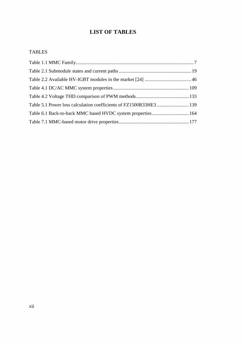
LIST OF TABLES
TABLES
Table 1.1 MMC Family ................................................................................................ 7
Table 2.1 Submodule states and current paths ........................................................... 19
Table 2.2 Available HV-IGBT modules in the market [24] ...................................... 46
Table 4.1 DC/AC MMC system properties .............................................................. 109
Table 4.2 Voltage THD comparison of PWM methods ........................................... 133
Table 5.1 Power loss calculation coefficients of FZ1500R33HE3 .......................... 139
Table 6.1 Back-to-back MMC based HVDC system properties .............................. 164
Table 7.1 MMC-based motor drive properties ......................................................... 177
xiii
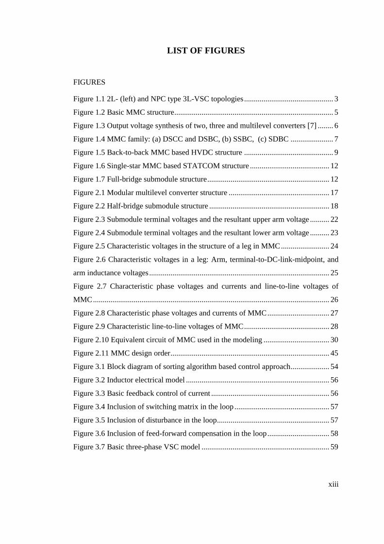
LIST OF FIGURES
FIGURES
Figure 1.1 2L- (left) and NPC type 3L-VSC topologies .............................................. 3
Figure 1.2 Basic MMC structure .................................................................................. 5
Figure 1.3 Output voltage synthesis of two, three and multilevel converters [7] ........ 6
Figure 1.4 MMC family: (a) DSCC and DSBC, (b) SSBC, (c) SDBC ...................... 7
Figure 1.5 Back-to-back MMC based HVDC structure .............................................. 9
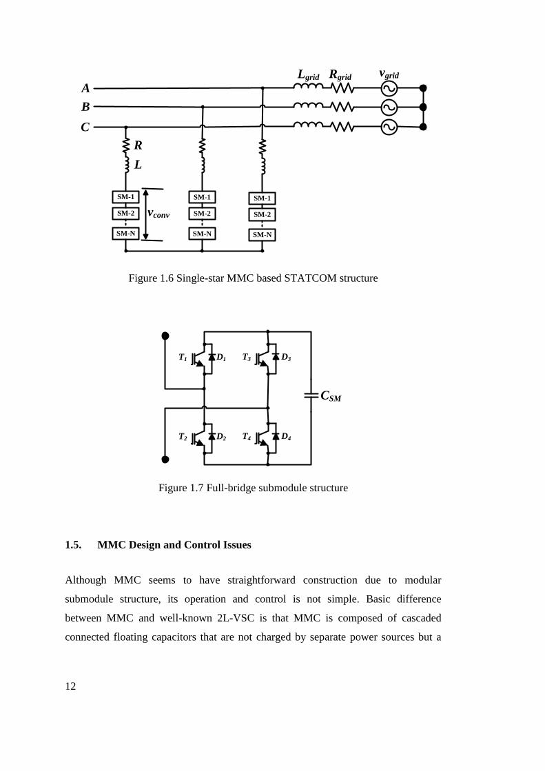
Figure 1.6 Single-star MMC based STATCOM structure ......................................... 12
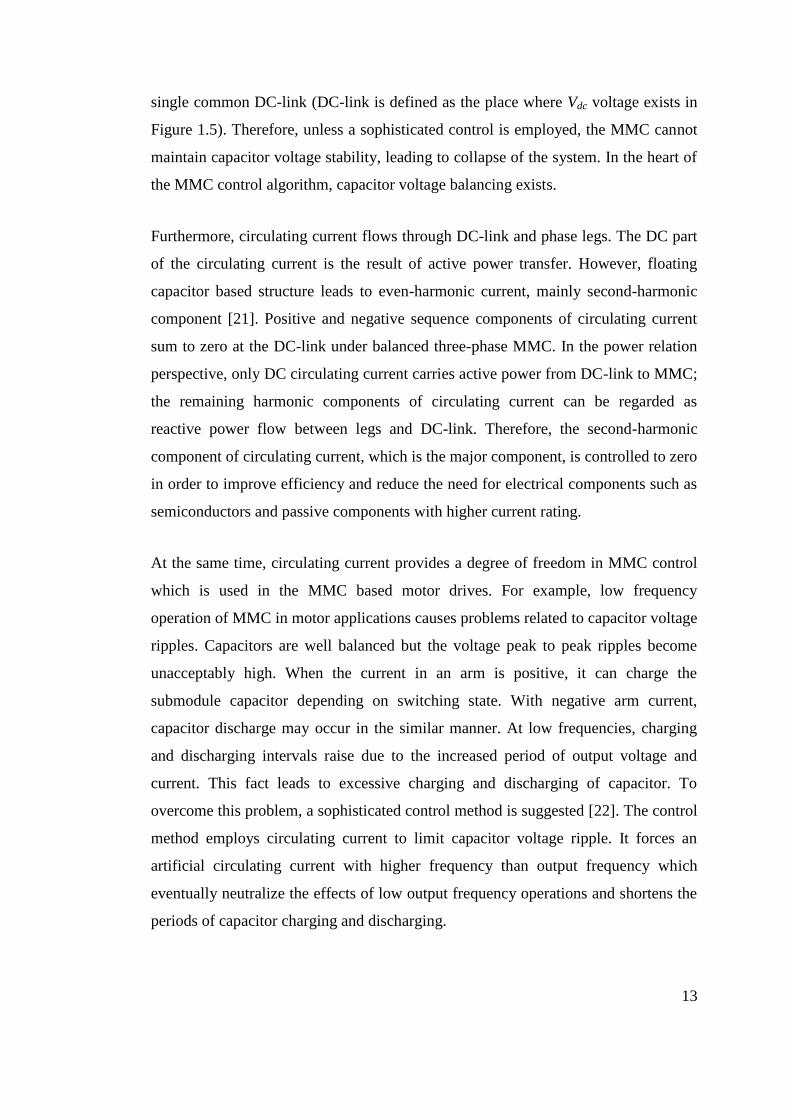
Figure 1.7 Full-bridge submodule structure ............................................................... 12
Figure 2.1 Modular multilevel converter structure .................................................... 17
Figure 2.2 Half-bridge submodule structure .............................................................. 18
Figure 2.3 Submodule terminal voltages and the resultant upper arm voltage .......... 22
Figure 2.4 Submodule terminal voltages and the resultant lower arm voltage .......... 23
Figure 2.5 Characteristic voltages in the structure of a leg in MMC ......................... 24
Figure 2.6 Characteristic voltages in a leg: Arm, terminal-to-DC-link-midpoint, and
arm inductance voltages ............................................................................................. 25
Figure 2.7 Characteristic phase voltages and currents and line-to-line voltages of
MMC .......................................................................................................................... 26
Figure 2.8 Characteristic phase voltages and currents of MMC ................................ 27
Figure 2.9 Characteristic line-to-line voltages of MMC ............................................ 28
Figure 2.10 Equivalent circuit of MMC used in the modeling .................................. 30
Figure 2.11 MMC design order .................................................................................. 45
Figure 3.1 Block diagram of sorting algorithm based control approach.................... 54
Figure 3.2 Inductor electrical model .......................................................................... 56
Figure 3.3 Basic feedback control of current ............................................................. 56
Figure 3.4 Inclusion of switching matrix in the loop ................................................. 57
Figure 3.5 Inclusion of disturbance in the loop.......................................................... 57
Figure 3.6 Inclusion of feed-forward compensation in the loop ................................ 58
Figure 3.7 Basic three-phase VSC model .................................................................. 59
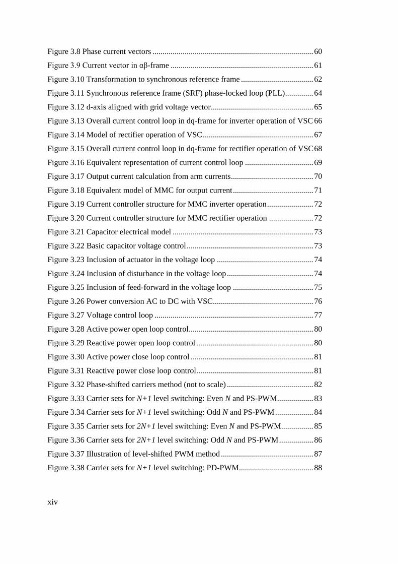
xiv
Figure 3.8 Phase current vectors ................................................................................ 60
Figure 3.9 Current vector in αβ-frame ....................................................................... 61
Figure 3.10 Transformation to synchronous reference frame .................................... 62
Figure 3.11 Synchronous reference frame (SRF) phase-locked loop (PLL) .............. 64
Figure 3.12 d-axis aligned with grid voltage vector ................................................... 65
Figure 3.13 Overall current control loop in dq-frame for inverter operation of VSC 66
Figure 3.14 Model of rectifier operation of VSC ....................................................... 67
Figure 3.15 Overall current control loop in dq-frame for rectifier operation of VSC 68
Figure 3.16 Equivalent representation of current control loop .................................. 69
Figure 3.17 Output current calculation from arm currents ......................................... 70
Figure 3.18 Equivalent model of MMC for output current ........................................ 71
Figure 3.19 Current controller structure for MMC inverter operation ....................... 72
Figure 3.20 Current controller structure for MMC rectifier operation ...................... 72
Figure 3.21 Capacitor electrical model ...................................................................... 73
Figure 3.22 Basic capacitor voltage control ............................................................... 73
Figure 3.23 Inclusion of actuator in the voltage loop ................................................ 74
Figure 3.24 Inclusion of disturbance in the voltage loop ........................................... 74
Figure 3.25 Inclusion of feed-forward in the voltage loop ........................................ 75
Figure 3.26 Power conversion AC to DC with VSC .................................................. 76
Figure 3.27 Voltage control loop ............................................................................... 77
Figure 3.28 Active power open loop control .............................................................. 80
Figure 3.29 Reactive power open loop control .......................................................... 80
Figure 3.30 Active power close loop control ............................................................. 81
Figure 3.31 Reactive power close loop control .......................................................... 81
Figure 3.32 Phase-shifted carriers method (not to scale) ........................................... 82
Figure 3.33 Carrier sets for N+1 level switching: Even N and PS-PWM .................. 83
Figure 3.34 Carrier sets for N+1 level switching: Odd N and PS-PWM ................... 84
Figure 3.35 Carrier sets for 2N+1 level switching: Even N and PS-PWM ................ 85
Figure 3.36 Carrier sets for 2N+1 level switching: Odd N and PS-PWM ................. 86
Figure 3.37 Illustration of level-shifted PWM method .............................................. 87
Figure 3.38 Carrier sets for N+1 level switching: PD-PWM ..................................... 88
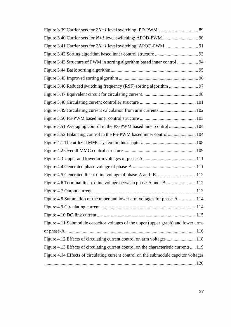
xv
Figure 3.39 Carrier sets for 2N+1 level switching: PD-PWM .................................. 89
Figure 3.40 Carrier sets for N+1 level switching: APOD-PWM ............................... 90
Figure 3.41 Carrier sets for 2N+1 level switching: APOD-PWM ............................. 91
Figure 3.42 Sorting algorithm based inner control structure ..................................... 93
Figure 3.43 Structure of PWM in sorting algorithm based inner control .................. 94
Figure 3.44 Basic sorting algorithm ........................................................................... 95
Figure 3.45 Improved sorting algorithm .................................................................... 96
Figure 3.46 Reduced switching frequency (RSF) sorting algorithm ......................... 97
Figure 3.47 Equivalent circuit for circulating current ................................................ 98
Figure 3.48 Circulating current controller structure ................................................ 101
Figure 3.49 Circulating current calculation from arm currents ................................ 102
Figure 3.50 PS-PWM based inner control structure ................................................ 103
Figure 3.51 Averaging control in the PS-PWM based inner control ....................... 104
Figure 3.52 Balancing control in the PS-PWM based inner control ........................ 104
Figure 4.1 The utilized MMC system in this chapter............................................... 108
Figure 4.2 Overall MMC control structure .............................................................. 109
Figure 4.3 Upper and lower arm voltages of phase-A ............................................. 111
Figure 4.4 Generated phase voltage of phase-A ...................................................... 111
Figure 4.5 Generated line-to-line voltage of phase-A and -B .................................. 112
Figure 4.6 Terminal line-to-line voltage between phase-A and -B .......................... 112
Figure 4.7 Output current ......................................................................................... 113
Figure 4.8 Summation of the upper and lower arm voltages for phase-A ............... 114
Figure 4.9 Circulating current .................................................................................. 114
Figure 4.10 DC-link current ..................................................................................... 115
Figure 4.11 Submodule capacitor voltages of the upper (upper graph) and lower arms
of phase-A ................................................................................................................ 116
Figure 4.12 Effects of circulating current control on arm voltages ......................... 118
Figure 4.13 Effects of circulating current control on the characteristic currents ..... 119
Figure 4.14 Effects of circulating current control on the submodule capcitor voltages
.................................................................................................................................. 120
xvi
Figure 4.15 Sorting method comparison on the upper-arm submodule capacitor
voltages of phase-A .................................................................................................. 122
Figure 4.16 Effects of 2N+1 level switching on voltage generation ....................... 124
Figure 4.17 Effect of 2N+1 level switching on leg voltage ..................................... 125
Figure 4.18 Effects of 2N+1 level switching on circulating current ........................ 126
Figure 4.19 FFT analysis of circulating current under 2N+1 level switching ......... 127
Figure 4.20 N+1 and 2N+1 level switching comparison with PD-PWM ................ 129
Figure 4.21 N+1 and 2N+1 level switching comparison with PS-PWM ................ 130
Figure 4.22 N+1 and 2N+1 level switching comparison with APOD-PWM .......... 131
Figure 5.1 Conduction loss calculation method ....................................................... 137
Figure 5.2 Switching loss calculation method ......................................................... 139
Figure 5.3 Total power loss in case of full active power transfer to grid ................. 142
Figure 5.4 Total power loss in case of full active power transfer to MMC ............. 143
Figure 5.5 Total power loss in case of full reactive power transfer to grid ............. 144
Figure 5.6 Total power loss in case of full reactive power transfer to MMC .......... 145
Figure 5.7 Individual semiconductor power losses: Active power transfer ............. 147
Figure 5.8 Individual semiconductor power losses: Reactive power transfer .......... 148
Figure 5.9 Semiconductor currents in case of PD-PWM, RSF sorting and
CSM=4mF: P=1pu (upper), Q=1pu (lower)............................................................. 150
Figure 5.10 Power loss frequency relation: PD-PWM and CSM=4mF, P=1pu ...... 151
Figure 5.11 Thermal model of a submodule semiconductors .................................. 152
Figure 5.12 Arm current and its asymmetry ............................................................ 153
Figure 5.13 Junction temperatures in a submodule: Active power transfer ............. 155
Figure 5.14 Junction temperatures in a submodule: Reactive power tranfer ........... 156
Figure 6.1 The back-to-back MMC system configuration ....................................... 159
Figure 6.2 DC-link equivalent circuit of back-to-back MMC system ..................... 160
Figure 6.3 Simplified DC-link equivalent circuit of back-to-back MMC system ... 161
Figure 6.4 Inverter-side MMC control ..................................................................... 162
Figure 6.5 Rectifier-side MMC control .................................................................... 163
Figure 6.6 DC-link current under "classical back-to-back converter control": without
(upper) and with (lower) power feed-forward at rectifier side ................................. 165
xvii
Figure 6.7 DC-link current under "proposed control method" ................................ 166
Figure 6.8 Id current of both rectifier and inverter MMCs ....................................... 166
Figure 6.9 Phase output currents: Rectifier (upper) and inverter (lower) MMCs .... 167
Figure 6.10 Submodule capacitor voltages: Rectifier (upper) and inverter side (lower)
.................................................................................................................................. 168
Figure 6.11 Average capacitor voltages of rectifier- and inverter-side MMCs ....... 169
Figure 6.12 DC-link voltage .................................................................................... 169
Figure 7.1 General control structure for low-frequency operation .......................... 176
Figure 7.2 Low-frequency output (motor) currents ................................................. 178
Figure 7.3 The forced circulating current in phase-A .............................................. 178
Figure 7.4 Submodule voltages: Upper (upper graph) and lower arm of phase-A .. 179
Figure 7.5 DC output current operation: Output current (upper) and submodule
capcitors in the upper arm (lower) ........................................................................... 180
Figure 7.6 Motor speed reference and actual values ................................................ 182
Figure 7.7 Electrical and load torque of the motor .................................................. 182
Figure 7.8 Motor current in abc- (upper) and dq-frame (lower) .............................. 183
Figure 7.9 Submodule capacitor voltages: Upper (upper graph) and lower arms ... 184
Figure A.1 MMC model for Chapter 4 .................................................................... 199
Figure A.2 MMC controller model .......................................................................... 200
Figure A.3 MMC model for Chapter 6 .................................................................... 201
Figure A.4 Simulation overview for Chapter 7 ........................................................ 202

xviii
LIST OF ABBREVIATIONS
AC Alternating Current
APOD Alternative Phase Opposition Disposition
DC Direct Current
HVDC High-Voltage Direct Current
IGBT Insulated Gate Bipolar Transistor
MMC Modular Multilevel Converter
PD Phase Disposition
POD Phase Opposition Disposition
PS Phase-shifted
PWM Pulse-width Modulation
SM Submodule
STATCOM Static Synchronous Compensator
THD Total Harmonic Distortion
VSC Voltage Source Converter
2L Two-level
3L Three-level

1
CHAPTER 1
1. INTRODUCTION
INTRODUCTION
1.1. Background
Energy is the vital input to all sides of economic activities. Factories, houses, cars,
trains etc. all need energy to function. With the transform in the world economic
structure throughout the last 2-3 centuries, energy demand has increased enormously.
The civilization began to substitute the man work force with machines with the
introduction of steam engine. Those days, main energy source was coal which was
burnt to produce controlled mechanical motion in factory machines or in trains.
However, the transmission of the generated energy was of limited capacity;
therefore, all fuel must be present at the load site. As a solution, electricity has
become the major intermediate form of energy due to its ease of transfer to the
consumers that are thousands of kilometers far from the generating unit. This feature
is hard to achieve for other forms of energy such as mechanical energy. Moreover,
electricity enabled the use of new energy sources such as hydroelectric dam and the
more efficient and economic use of existing energy sources such as coal.
Hydroelectric generators should be established on rivers which may be very far from
major consumers. Since electricity can efficiently be transmitted over long distances,
the mechanical energy in the running water is transformed to electrical energy in the
dam. For example, the rivers in southwest of Turkey have large power potential but
are far from major cities. With the help of newly built dams and electrical power

2
transmission lines, the consumers make use of a remote and cheap energy source. In
addition, electricity enabled the use the coal energy at the mine site. This eliminated
the transportation of coal to the consumer site and enabled the scale of economy and
improved technical and economic efficiency. Because the electricity is the basic
available energy, factories, offices and houses are full of electrical tools and
machines. Therefore, it can be said that the modern civilization based its operations
on electricity, resulting ever increasing energy demand. Indeed, the world energy
consumption is projected to increase by more than 54% every decade [1].
However, the available electricity in the utility grid is not always at desired form.
Sometimes voltage, sometimes frequency or sometimes both quantities are desired to
be different than what is presented by the utility. Power electronics is an area of
electrical engineering that deals with transforming the electrical energy to the form
that the load can work. Traditionally, power supplies for electronic circuits and speed
controllers for electrical machines have been the major application area of power
electronics.
Today, energy supply still is based on the fossil sources such as coal, natural gas and
petroleum, although they are generally burnt to generate electricity. Growing
awareness about environmental issues has led people to look for alternative energy
sources because fossil sources pollute the environment by releasing greenhouse gases
when burnt. Therefore, the support for the renewable energy sources came into place.
Wind and solar energies are among the popular ones. Power electronics becomes the
enabler technology for renewable energy integration. In both energy sources, the
primitive energy form is not appropriate for grid integration. For example, solar
panels generate low DC voltages with variable power output. Power electronics
circuits extract maximum power possible from solar panels and inject that power to
grid fulfilling the strict grid codes. In addition, recent developments in electric
vehicles are another effort in order to limit greenhouse gas emission. Again, power
electronics is the key technology. The main application here is motor drive and
battery charger. Efficient, reliable, and cheap solutions are at the target.
3
In the light of the ongoing transformation of the way that electrical energy is
generated and consumed, it can be said that power electronics is at the core of this
transformation. Therefore, it should be more reliable, efficient, and affordable.
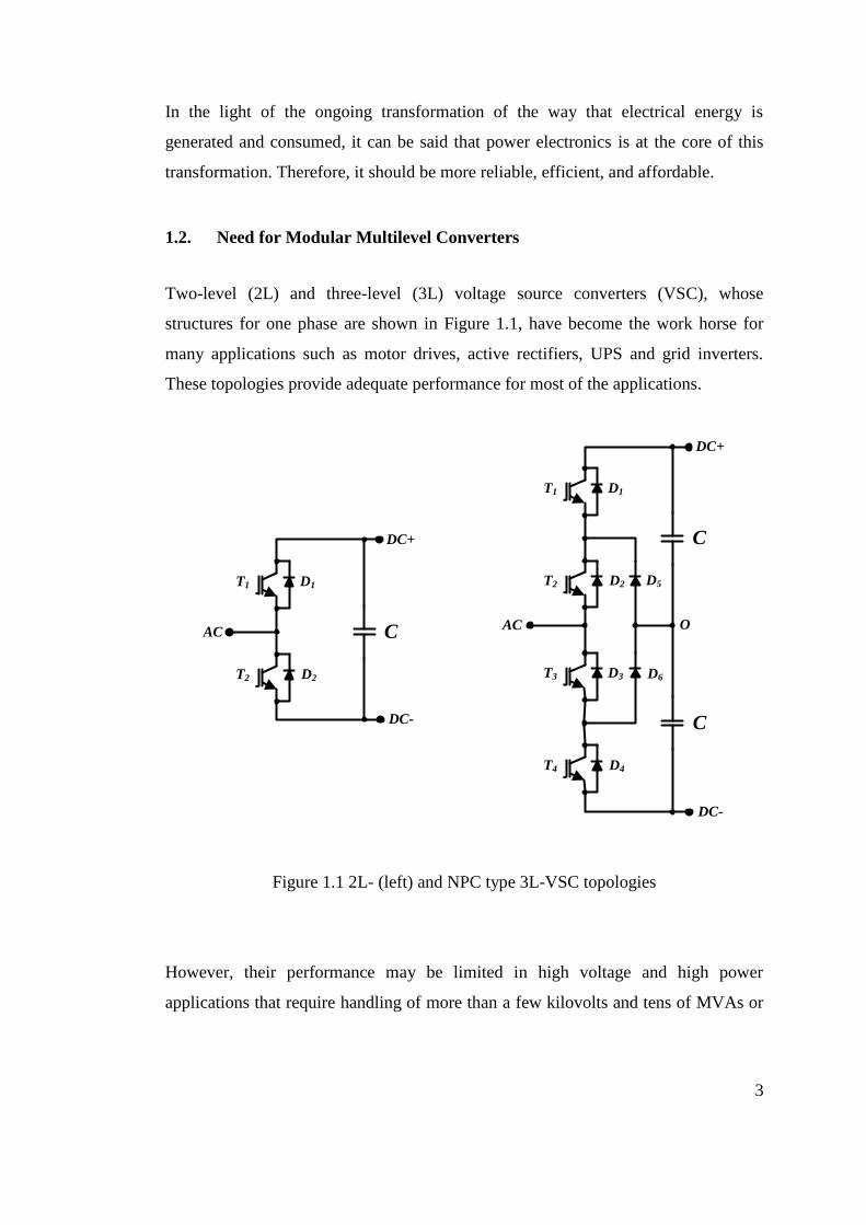
1.2. Need for Modular Multilevel Converters
Two-level (2L) and three-level (3L) voltage source converters (VSC), whose
structures for one phase are shown in Figure 1.1, have become the work horse for
many applications such as motor drives, active rectifiers, UPS and grid inverters.
These topologies provide adequate performance for most of the applications.
DC+
AC C
T2
D1
D2
T1
DC-
C
T2
D1
D2
T1
C
T4
D3
D4
T3
D5
D6
OAC
DC+
DC-
Figure 1.1 2L- (left) and NPC type 3L-VSC topologies
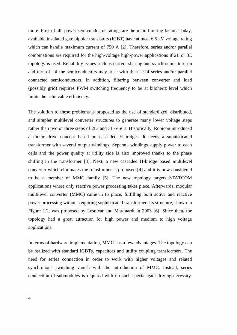
However, their performance may be limited in high voltage and high power
applications that require handling of more than a few kilovolts and tens of MVAs or
4
more. First of all, power semiconductor ratings are the main limiting factor. Today,
available insulated gate bipolar transistors (IGBT) have at most 6.5 kV voltage rating
which can handle maximum current of 750 A [2]. Therefore, series and/or parallel
combinations are required for the high-voltage high-power applications if 2L or 3L
topology is used. Reliability issues such as current sharing and synchronous turn-on
and turn-off of the semiconductors may arise with the use of series and/or parallel
connected semiconductors. In addition, filtering between converter and load
(possibly grid) requires PWM switching frequency to be at kilohertz level which
limits the achievable efficiency.
The solution to these problems is proposed as the use of standardized, distributed,
and simpler multilevel converter structures to generate many lower voltage steps
rather than two or three steps of 2L- and 3L-VSCs. Historically, Robicon introduced
a motor drive concept based on cascaded H-bridges. It needs a sophisticated
transformer with several output windings. Separate windings supply power to each
cells and the power quality at utility side is also improved thanks to the phase
shifting in the transformer [3]. Next, a new cascaded H-bridge based multilevel
converter which eliminates the transformer is proposed [4] and it is now considered
to be a member of MMC family [5]. The new topology targets STATCOM
applications where only reactive power processing takes place. Afterwards, modular
multilevel converter (MMC) came in to place, fulfilling both active and reactive
power processing without requiring sophisticated transformer. Its structure, shown in
Figure 1.2, was proposed by Lesnicar and Marquardt in 2003 [6]. Since then, the
topology had a great attraction for high power and medium to high voltage
applications.
In terms of hardware implementation, MMC has a few advantages. The topology can
be realized with standard IGBTs, capacitors and utility coupling transformers. The
need for series connection in order to work with higher voltages and related
synchronous switching vanish with the introduction of MMC. Instead, series
connection of submodules is required with no such special gate driving necessity.
5
Likewise IGBTs, capacitors can be selected from existing products, with no
requirement of series connection or very high voltage rating.
SM-1
SM-2
SM-N
SM-1
SM-2
SM-N
O
SM-1
SM-2
SM-N
SM-1
SM-2
SM-N
SM-1
SM-2
SM-N
SM-1
SM-2
SM-N
½Vdc
½Vdc
A
B
C
Figure 1.2 Basic MMC structure
In addition, multilevel nature of MMC improves the waveform quality at the output.
The conventional 2L- and 3L-VSCs cause high harmonic distortion in the output
voltage waveform of the converter. Therefore; the need for higher PWM switching
frequency and/or larger output harmonic filter arise which increase the cost, power
loss, and footprint of the system. On the other hand, MMC topology relies on many
small voltage steps at the output which lowers harmonic distortion. This advantage
results in employing lower PWM switching frequency and hence improved
efficiency and lower investment on the cooling system. In addition, MMC greatly
reduces or removes the need of harmonic filter at the output. Output voltage

6
synthesis concepts of two, three and multilevel converters are illustrated in Figure
1.3
Figure 1.3 Output voltage synthesis of two, three and multilevel converters [7]
Moreover, the distributed submodule structure provides a more reliable operation and
eases fault diagnosis and maintenance. Especially in faulty conditions, the distributed
configuration with redundant submodules may allow control algorithm to locate and
isolate the faulty submodules and to maintain almost normal operation in many
cases.
Compared to conventional 2L- and 3L-VSC technologies, MMC offers advantages
such as simple construction with half-bridge submodules based on standard IGBT
and capacitor, modular and redundant construction, longer maintenance intervals,
improved reliability, higher efficiency, and lower filtering requirement.
1.3. MMC Classification
Akagi classified the MMC family in [5] according to using chopper or full-bridge
submodules and being delta or star structure. The topology may adopt chopper (half-
bridge) or full-bridge based submodules. In addition, the arms can be connected in
7
star or delta. The possibilities are summarized in Table 1.1. Some of the possible
topologies cannot practically implemented in AC applications. Therefore, there are
four practical members of this family.
Table 1.1 MMC Family
Star Delta
Single Double Single Double
Chopper x x x
Full-bridge x
The members of this family are visualized in Figure 1.4 and given as:
i. Single-Star Bridge-Cell (SSBC)
ii. Single-Delta Bridge-Cell (SDBC)
iii. Double-Star Chopper-Cell (DSCC)
iv. Double-Star Bridge-Cell (DSBC)
SM 1-N
SM 1-N
SM 1-N
SM 1-N
SM 1-N
SM 1-N
Vdc
SM 1-NSM 1-NSM 1-N SM 1-NSM 1-NSM 1-N
(a) (b) (c)
A
B
C
Figure 1.4 MMC family: (a) DSCC and DSBC, (b) SSBC, (c) SDBC
8
Three of these topologies are based on bridge cell. Only DSCC utilizes chopper cell.
Many researchers on this topic prefer to use MMC term to refer DSCC topology.
Therefore, this thesis mostly refers to DSCC when saying MMC.
1.4. Typical MMC Application Areas
MMC targets high-power and high-voltage applications such as high-voltage direct
current (HVDC) transmission systems, STATCOM applications, and also gradually
medium-voltage motor drives.
1.4.1. HVDC Application
High voltage direct current (HVDC) transmission systems utilize direct current for
the bulk transmission of electrical power. It is an alternative to the three-phase AC
transmission of electric power, especially for several specific conditions. For
example, HVDC transmission is preferred for the applications of transmission under
water, energy trade between countries and transmission over long distances.
Today, HVDC technology has transformed from thyristor based line commutated
current source converters (LCC) to 2L- and 3L-VSCs [8], and finally to modular
multilevel converters, shown in Figure 1.5. The converters may be placed in the
same site with zero DC line which is named as back-to-back HVDC. Alternatively, a
DC line can also be used. Currently, MMC is utilized as HVDC technology with
commercial names Siemens’s "HVDC Plus" [7], ABB’s 4th
generation "HVDC
Light” [9] and Alstom’s "HVDC MaxSine" [10].

9
Rgrid_i vgrid_iLgrid_i
SM 1-N
SM 1-N
SM 1-N
SM 1-N
SM 1-N
SM 1-N
SM 1-N
SM 1-N
SM 1-N
SM 1-N
SM 1-N
SM 1-N
Rgrid_rvgrid_r Lgrid_r
Vdc
RECTIFIER INVERTERidc
P, QP, Q
Figure 1.5 Back-to-back MMC based HVDC structure
Underwater power transmission is realized with power cables. If the cables are
excited by AC voltage, large capacitive currents are required to charge and discharge
the cable parasitic capacitance in every cycle. However, HVDC systems do not
suffer from capacitive cable currents. Therefore, although the converters in HVDC
cause extra investment compared to AC system, it may economically be justified for
ranges about 50 km cable [11]. As an example, in 2010, the first MMC based HVDC
system, the Trans Bay Cable, is built in California, the USA, between San Francisco
and Pittsburg. The system has 85-km-long power cables laid down under San
Francisco Bay [12]. It has a 400 MW power rating and ±200 kV DC line voltage.
The HVDC system can supply up to ±145 MVAr reactive power at the Pittsburg and
up to ±170 MVAr reactive power at the San Francisco to support local grids. In
addition, recently several offshore wind firms have been built in North Sea [13]. The
generated hundreds of MW power should be transmitted to the grid on the land with
underwater cables. The MMC based HVDC technology is employed in these projects
such as BorWin, DolWin, HelWin, and SylWin [14].
Countries exchange electrical power for several reasons such as electricity trade and
power system stability. HVDC can also be used for electrical power exchange
10
between countries. These grids may be unsynchronized or even adopt different
frequencies such as 50 and 60 Hz. If different frequencies are utilized,
synchronization of the two grids is not possible; therefore, HVDC is the only way to
exchange power. Therefore, power system stability may be increased via the use of
HVDC systems between the 50 and 60 Hz regions. The basic advantage of HVDC
over the AC transmission in this context is the ability of controlling active power
transmission accurately, while AC line power flow cannot be controlled in the same
direct way. One example of MMC based HVDC between countries is the INELFE,
built between France [15]. There are two parallel links; each has 1000 MW power
capacity. The ±320 kV DC-link has 65-km-long underground cable.
Another usage of HVDC system is to transmit bulk power over very long distances.
In [11], it is shown that the cost of HVDC may be justified about 800 km overhead
line. General advantages for choosing HVDC transmission instead of three-phase AC
transmission can be as follows: lower transmission losses, the capacity to transfer
more power over the same right of way and so on.
1.5.2. Motor Drive Application
The medium-voltage drives cover power ratings from 250 kW to more than 100 MW
at the medium-voltage (MV) level of 2.3 to 13.8 kV. However, the majority of the
installed MV drives are in the 1 to 4 MW range with voltage ratings from 3.3 kV to
6.6 kV [16].
Medium-voltage motor drive is another candidate for MMC application. However,
low frequency operation of the topology is problematic. The reason basically lies in
the capacitors which are floating. Since the capacitor voltages are affected by load
current due to their floating nature, the voltage ripple of the capacitors increases at
low frequencies. Therefore, it is generally thought that fan and pump type loads
which need low torque at low speeds (low operating frequencies) and higher torque
at higher speeds are the typical application candidates for MMC based motor drives

11
[17]. In this way, the load less upsets the MMC and leaves some room to extra
control effort to limit voltage ripple of the capacitors for low speeds. Higher speed
operation is already not problematic. Currently, commercialization of MMC based
motor drives is not as wide spread as in HVDC case. Benshaw, Inc. of Regal-Beloit
Corporation, a motor drive manufacturer in the USA, claims to have a commercial
MMC based motor drive. The M2L 3000 Series drive targets 2.3 to 6.6 kV voltage
level with 300 to 10000 hp power rating [18].
1.5.3. STATCOM Application
Single-star or single-delta full-bridge structure of MMC family may be used in
STATCOM applications [5]. In addition to these topologies, HVDC system is also
capable of functioning as STATCOM.
Static synchronous compensator (STATCOM) is a VSC based reactive power
regulator. It is used to regulate and improve the stabilization of AC power grids.
STATCOM is built to support the grids which have lower power factor and voltage
regulation problems. Historically, the function of STATCOM was carried out by the
synchronous machines with special field excitation which freely spins without
mechanical load and later by thyristor based static VAR compensator (SVC).
The STATCOM based on the topologies in MMC family improves the dynamic
stability of the transmission systems and power quality and provides flexibility for
the designs with various power ratings and the compact design with low footprint as
well as redundancy. It behaves as variable impedance load with variable power
factor. The single-star structure is shown in Figure 1.6 with its submodule in Figure
1.7. Some manufacturers have commercial STATCOM systems such as Siemens’s
“SVC Plus” [19] and ABB’s “SVC Light” [20].
12
SM-1
SM-2
SM-N
Rgrid vgrid
vconv
SM-1
SM-2
SM-N
Lgrid
SM-1
SM-2
SM-N
R
L
A
B
C
Figure 1.6 Single-star MMC based STATCOM structure
CSM
T2
D1
D2
T1
T4
T3 D3
D4
Figure 1.7 Full-bridge submodule structure
1.5. MMC Design and Control Issues
Although MMC seems to have straightforward construction due to modular
submodule structure, its operation and control is not simple. Basic difference
between MMC and well-known 2L-VSC is that MMC is composed of cascaded
connected floating capacitors that are not charged by separate power sources but a
13
single common DC-link (DC-link is defined as the place where Vdc voltage exists in
Figure 1.5). Therefore, unless a sophisticated control is employed, the MMC cannot
maintain capacitor voltage stability, leading to collapse of the system. In the heart of
the MMC control algorithm, capacitor voltage balancing exists.
Furthermore, circulating current flows through DC-link and phase legs. The DC part
of the circulating current is the result of active power transfer. However, floating
capacitor based structure leads to even-harmonic current, mainly second-harmonic
component [21]. Positive and negative sequence components of circulating current
sum to zero at the DC-link under balanced three-phase MMC. In the power relation
perspective, only DC circulating current carries active power from DC-link to MMC;
the remaining harmonic components of circulating current can be regarded as
reactive power flow between legs and DC-link. Therefore, the second-harmonic
component of circulating current, which is the major component, is controlled to zero
in order to improve efficiency and reduce the need for electrical components such as
semiconductors and passive components with higher current rating.
At the same time, circulating current provides a degree of freedom in MMC control
which is used in the MMC based motor drives. For example, low frequency
operation of MMC in motor applications causes problems related to capacitor voltage
ripples. Capacitors are well balanced but the voltage peak to peak ripples become
unacceptably high. When the current in an arm is positive, it can charge the
submodule capacitor depending on switching state. With negative arm current,
capacitor discharge may occur in the similar manner. At low frequencies, charging
and discharging intervals raise due to the increased period of output voltage and
current. This fact leads to excessive charging and discharging of capacitor. To
overcome this problem, a sophisticated control method is suggested [22]. The control
method employs circulating current to limit capacitor voltage ripple. It forces an
artificial circulating current with higher frequency than output frequency which
eventually neutralize the effects of low output frequency operations and shortens the
periods of capacitor charging and discharging.
14
In the outer control loops, similar techniques to control 2L-VSC can be applied. This
may include power control, DC-link voltage control and motor speed control.
In the design of MMC, passive component sizing is important. Submodule capacitors
may be chosen considering peak-to-peak voltage ripple under specific operating
conditions such as power level and frequency. Arm inductor and submodule
capacitor creates resonant frequencies; therefore, when designing the passive
components, attention should be paid not to create these frequencies at operation
frequency.
1.6. Scope of the Thesis
The focus of the thesis is the control and modulation of MMC for HVDC and motor
drive applications. In addition, power loss and thermal characterization of MMC are
emphasized. It is supported by detailed computer simulations.
The main objectives of this thesis are:
i. Studying the basic principles of MMC.
ii. Examining control methods of MMC
iii. Analysis of MMC applications such as HVDC and motor drive.
iv. Characterization of power loss and thermal behavior.
This thesis consists of 8 chapters.
Chapter 2 gives the mathematical model and circuit analysis of MMC. Topological
structure and operation of the converter is provided in detail. Analytical modeling of
inner operation of MMC is provided. It also discusses the component sizing of
MMC. Number of submodules per arm, IGBT electrical parameters, submodule
capacitor, and arm inductor values are the fundamental design issues of MMC.
15
In Chapter 3, the control of MMC is considered. Outer control loops including output
current control, power control, and DC-link voltage control, are studied. Also,
several multilevel PWM methods are reviewed. Carrier based PWM methods, level-
shifted and phase-shifted PWM, and nearest-level modulation are detailed.
Afterwards, inner control aspects of MMC, namely capacitor voltage balancing and
circulating current control, are discussed. The mostly acknowledged control
approaches in the literature, sorting algorithm and phase-shifted carrier PWM based
control, are detailed.
In Chapter 4, the control and modulation methods described in the previous chapter
are visualized on a sample MMC system. The application of circulating current
control, sorting algorithm methods, and modulation techniques on the converter are
observed on a sample DC/AC MMC and their electrical effects are evaluated.
In Chapter 5, the power loss and thermal characterization of MMC are studied. First
of all, the total system and individual semiconductor power losses are characterized
for the conditions of circulating current control employment, different PWM
methods, power factor, sorting methods, submodule capacitance values and PWM
frequency. In addition, the temperature behaviors of the individual semiconductors
are provided for various conditions. The reason behind the asymmetric power loss
among the semiconductors in a submodule is shown.
In Chapter 6, back-to-back connected MMC whose possible application area includes
HVDC is presented. An improvement to classical control approach of back-to-back
converter is proposed and overall control of back-to-back connected MMC is
described. The performance of the new control approach is shown on a sample
system via MATLAB/Simulink.
In Chapter 7, the intrinsic problem of the topology in low-frequency operation is
clarified and the solution to this problem in the literature is provided. At last, after
16
adapting this control method, MMC based motor drive which dynamically or
statically operates in low-frequency region is verified via simulation.
Finally, the thesis concludes with a summary of information and experience gained
throughout the study. Developments and future work are also addressed.

17
CHAPTER 2
2. MODULAR MULTILEVEL CONVERTER BASICS
MODULAR MULTILEVEL CONVERTER BASICS
2.1. Basics and Definitions
Modular multilevel converter (MMC), shown in Figure 2.1, is based on the series
connection of the identical submodules.
SM-1
SM-2
SM-N
SM-1
SM-2
SM-N
Larm
Rarm Rgrid vgrid
NO
iO
vL
vU
iL
iU
SM-1
SM-2
SM-N
SM-1
SM-2
SM-N
Lgrid
SM-1
SM-2
SM-N
SM-1
SM-2
SM-N
Rarm
Larm
Arm LegSubmodule
½Vdc
½Vdc
Load
Figure 2.1 Modular multilevel converter structure
18
Submodule is the basic building block of MMC, shown in Figure 2.2. The
modularity of modular multilevel converter comes from this basic building block.
Each submodule has a well-known half-bridge structure, which consists of one
submodule capacitor and two power semiconductors, IGBT.
VSM
T2
D1
D2
T1
CSM
+
_
Figure 2.2 Half-bridge submodule structure
The capacitor acts as the DC-link capacitor of two-level (2L) converter, but it is
evenly distributed in the structure of MMC. It behaves as a voltage source and
energy buffer. The half-bridge IGBTs chop the capacitor voltage according to PWM
commands. The transistors T1 and T2 in the submodule work in an opposite way.
When T1 is turned on, T2 has to be turned off to prevent shoot-through. When T1 is
turned on, the capacitor voltage appears at the submodule terminals. In this
condition, the submodule is said to be "inserted". Otherwise, it is said to be
"bypassed".
A three-phase 2L converter involves six power semiconductors. MMC replaces each
semiconductor in the 2L converter with a structure of a cascaded submodules and an
inductor, shown in Figure 2.1. This structure is called arm. The structure of cascaded
submodules are the basic motive of "multi level" voltage appearing at the output. The
arm above the output terminal is named upper arm, and the below is named lower
arm. The arm inductor isolates the upper and lower arm when they switching and
19
prevents higher current flow between these two arms. The inductor acts as a filter
also for output current.
The upper and lower arm forms a leg which is the hardware section of MMC for one
phase. Three legs constitute a three-phase MMC as shown in Figure 2.1. The legs are
connected to a common DC-link.
In the Table 2.1, possible conditions of the arm current (either iU or iL) direction and
the gate signals of submodule semiconductors are summarized.
Table 2.1 Submodule states and current paths
T1=ON, T2=OFF T1=OFF, T2=ON T1=OFF, T2=OFF
iarm
>0
CSM
T2
D1
D2
T1
iarm
iarmCSM
T2
D1
D2
T1
CSM
T2
D1
D2
T1
iarm
iarm
<0
CSM
T2
D1
D2
T1
iarm
CSM
T2
D1
D2
T1
iarm
CSM
T2
D1
D2
T1
iarm
It can be deduced that charging and discharging of submodule capacitor occur when
T1 is turned on. If the arm current is positive, then the capacitor is charged. This fact
will be useful when discussing capacitor voltage balancing in Section 3.6. In
addition, the conditions where both IGBTs are off-state may represent initial
charging of submodule capacitor during start-up.

20
2.2. MMC Working Principle
Although the working principle of MMC is more complex, its basis may be
attributed to the basic 2L-VSC. Different from the 2L converter, the output voltage is
built by several steps depending on the submodule number. As the modulator
translates the control signals into the gate signals to the IGBTs, some of the
submodules are inserted and the remaining ones are bypassed to generate desired
voltage at the output. This comes from being multilevel converter.
Another important point to mention is the capacitors in submodules that are not fed
by an external power source. Therefore, they are called floating. Charging and
discharging should cancel out each other over a period and all submodule capacitor
voltages should be close or ideally equal to each other. Therefore, capacitor voltages
in an arm should be equalized in all the operating time by an active balancing
control. In any proposed control method, the balancing basically depends on the
current paths and the states given in Table 2.1. For example, if it is desired to
increase the voltage of a submodule, then its on-duration may be increased when arm
current is positive. As the Table 2.1 shows, the condition of turned-on T1 determines
the charging process. Also, turn-on of a submodule is equivalent o turn-on of T1. As
a result, the charging of a submodule capacitor is coupled with insertion of
submodules.
In addition to the voltage balancing, MMC has another important aspect, circulating
current. When MMC transfers active power to load, the energy is supplied from the
submodule capacitors. The only way to recover the lost energy to output or losses is
the power coming from the common DC-link. Therefore, a circulating current
naturally flows through the leg in addition to output current, shown in Figure 2.10.
The circulating current is common in both upper and lower arm. The DC part of this
current compensates the lost energy of the capacitors. However, due to the floating
nature of the capacitors, the circulating current at other harmonics, mainly second

21
harmonic, also flow. The second-harmonic component may be controlled to zero.
This control is independent from output current control.
After the internal aspects of MMC explained above, characteristic voltages should be
investigated to better understand how MMC is working. Output voltage generation
of MMC is based on the six arm voltages. All arm voltages are synthesized
independently with their own PWM carrier sets. However, the reference signals, of
course, are generated from a single controller.
To visualize the voltage generation mechanism in MMC, from submodule to arm and
then phase voltages are investigated. The waveforms belong to a 5-SM MMC as it is
mainly used in coming chapters. Voltages and current are not explicit; therefore,
average submodule voltage is taken as voltage unit. In Figure 2.3, the terminal
voltages of each submodule in the upper arm are shown. When the all terminal
voltages of the submodules in the arm are summed, the resultant upper arm voltage
between the nodes P and AU is found and described with the graph at the bottom of
Figure 2.3. Here, P denotes the positive terminal of DC-link and AU is the node
described on MMC in Figure 2.6. The arm voltage ranges from zero to DC-link
voltage in a sinusoidal way and has N+1 levels (here it has six levels). That means
they have offset equal to the half of the DC-link voltage. When the upper and lower
arm voltages have 180-degree phase shift, the phase terminal voltage will not have
the DC offset. Therefore, the voltage references to upper and lower arms are
consciously shifted 180-degree apart. Any control signal related to output current,
voltage, or power should have this 180-degree phase-shift between the upper and
lower arms. On the other hand, inner control signals such as circulating current are
common for both arms.
22
SM-1
SM-2
SM-3
SM-4
SM-5
P
AU
1 1.005 1.01 1.015 1.02 1.025 1.03 1.035 1.04
0
0.5
1
SM
-1 O
utp
ut V
olta
ge
[pu
]
1 1.005 1.01 1.015 1.02 1.025 1.03 1.035 1.040
1
2
3
4
5
6
Arm
Vo
ltag
e [p
u]
Time [s]
1 1.005 1.01 1.015 1.02 1.025 1.03 1.035 1.04
0
0.5
1
SM
-2 O
utp
ut V
olta
ge
[pu
]
1 1.005 1.01 1.015 1.02 1.025 1.03 1.035 1.04
0
0.5
1
SM
-3 O
utp
ut V
olta
ge
[pu
]
1 1.005 1.01 1.015 1.02 1.025 1.03 1.035 1.04
0
0.5
1
SM
-4 O
utp
ut V
olta
ge
[pu
]
1 1.005 1.01 1.015 1.02 1.025 1.03 1.035 1.04
0
0.5
1
SM
-5 O
utp
ut V
olta
ge
[pu
]
Figure 2.3 Submodule terminal voltages and the resultant upper arm voltage
The terminal voltages of the lower arm submodules are visualized in Figure 2.4.
When the all terminal voltages of the submodules in the arm are summed, the
resultant lower arm voltage between the nodes AL and N is given at the bottom of the
graph. Here, N denotes the negative terminal of DC-link and AL is the node
described on MMC in Figure 2.6.

23
SM-1
SM-2
SM-3
SM-4
SM-5
AL
N
1 1.005 1.01 1.015 1.02 1.025 1.03 1.035 1.040
1
2
3
4
5
6
Arm
Vo
ltag
e [p
u]
Time [s]
1 1.005 1.01 1.015 1.02 1.025 1.03 1.035 1.04
0
0.5
1
SM
-1 O
utp
ut V
olta
ge
[pu
]
1 1.005 1.01 1.015 1.02 1.025 1.03 1.035 1.04
0
0.5
1S
M-2
Outp
ut V
olta
ge
[pu
]
1 1.005 1.01 1.015 1.02 1.025 1.03 1.035 1.04
0
0.5
1
SM
-3 O
utp
ut V
olta
ge
[pu
]
1 1.005 1.01 1.015 1.02 1.025 1.03 1.035 1.04
0
0.5
1
SM
-4 O
utp
ut V
olta
ge
[pu
]
1 1.005 1.01 1.015 1.02 1.025 1.03 1.035 1.04
0
0.5
1
SM
-5 O
utp
ut V
olta
ge
[pu
]
Figure 2.4 Submodule terminal voltages and the resultant lower arm voltage
After describing submodule- and arm-level characteristic voltages, leg-level voltages
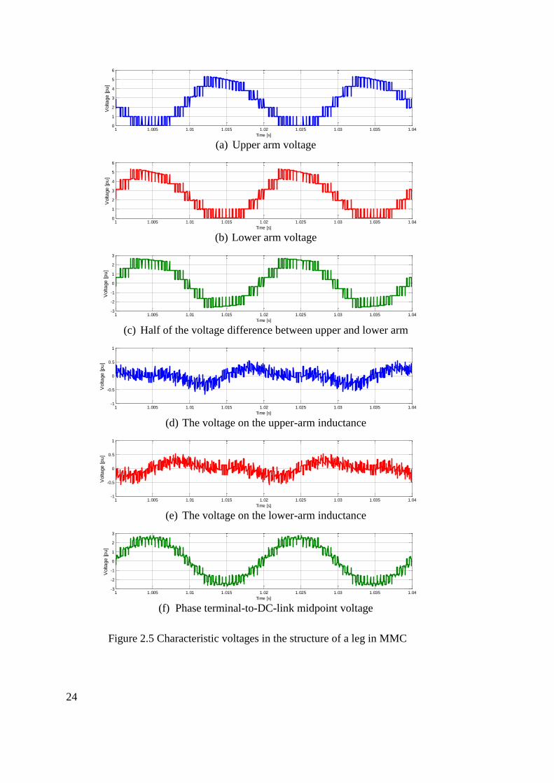
are now visualized in Figure 2.5. Arm voltages, arm inductance voltages and also the
resultant phase terminal-to-DC-link-midpoint are given.
24
(a) Upper arm voltage
(b) Lower arm voltage
(c) Half of the voltage difference between upper and lower arm
(d) The voltage on the upper-arm inductance
(e) The voltage on the lower-arm inductance
(f) Phase terminal-to-DC-link midpoint voltage
Figure 2.5 Characteristic voltages in the structure of a leg in MMC
1 1.005 1.01 1.015 1.02 1.025 1.03 1.035 1.040
1
2
3
4
5
6
Volta
ge
[p
u]
Time [s]
1 1.005 1.01 1.015 1.02 1.025 1.03 1.035 1.040
1
2
3
4
5
6
Volta
ge
[p
u]
Time [s]
1 1.005 1.01 1.015 1.02 1.025 1.03 1.035 1.04-3
-2
-1
0
1
2
3
Volta
ge
[p
u]
Time [s]
1 1.005 1.01 1.015 1.02 1.025 1.03 1.035 1.04-1
-0.5
0
0.5
1
Volta
ge
[p
u]
Time [s]
1 1.005 1.01 1.015 1.02 1.025 1.03 1.035 1.04-1
-0.5
0
0.5
1
Volta
ge
[p
u]
Time [s]
1 1.005 1.01 1.015 1.02 1.025 1.03 1.035 1.04-3
-2
-1
0
1
2
3
Volta
ge
[p
u]
Time [s]
25
SM-1
SM-2
SM-3
SM-1
SM-2
O
SM-1
SM-2
SM-3
SM-1
SM-2
SM-1
SM-2
SM-1
SM-2
½Vdc
½Vdc
BA
SM-4
SM-5
SM-4
SM-5
SM-3
SM-4
SM-5
SM-3
SM-4
SM-5
SM-3
SM-4
SM-5
SM-3
SM-4
SM-5
C
1 1.01 1.02 1.03 1.04-3
-2
-1
0
1
2
3
Time [s]
Volt
age
[p
u]
1 1.01 1.02 1.03 1.040
1
2
3
4
5
6
Time [s]V
olt
age
[p
u]
1 1.01 1.02 1.03 1.040
1
2
3
4
5
6
Time [s]
Volt
age
[p
u]
1 1.005 1.01 1.015 1.02 1.025 1.03 1.035 1.04-1
-0.5
0
0.5
1
Volta
ge
[p
u]
Time [s]
1 1.005 1.01 1.015 1.02 1.025 1.03 1.035 1.04-1
-0.5
0
0.5
1
Volta
ge
[p
u]
Time [s]
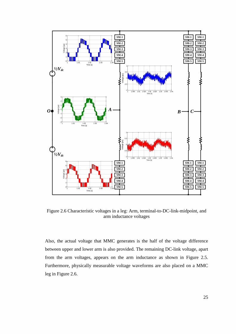
Figure 2.6 Characteristic voltages in a leg: Arm, terminal-to-DC-link-midpoint, and
arm inductance voltages
Also, the actual voltage that MMC generates is the half of the voltage difference
between upper and lower arm is also provided. The remaining DC-link voltage, apart
from the arm voltages, appears on the arm inductance as shown in Figure 2.5.
Furthermore, physically measurable voltage waveforms are also placed on a MMC
leg in Figure 2.6.
26
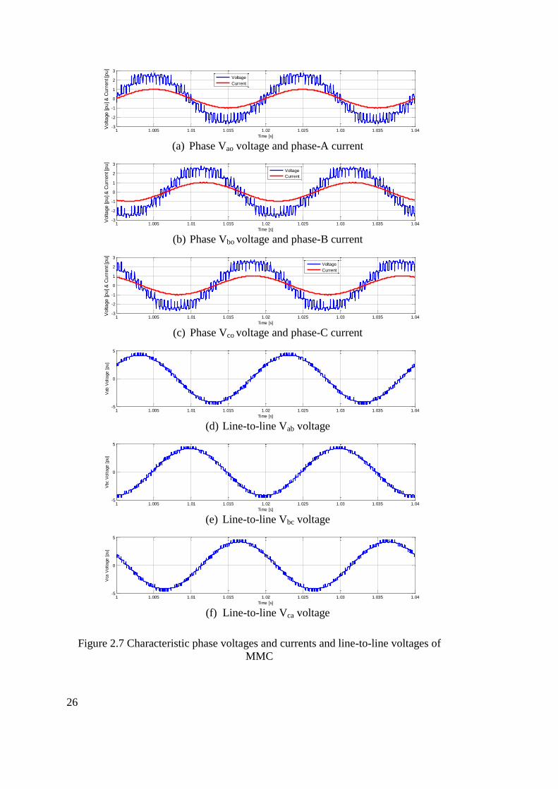
(a) Phase Vao voltage and phase-A current
(b) Phase Vbo voltage and phase-B current
(c) Phase Vco voltage and phase-C current
(d) Line-to-line Vab voltage
(e) Line-to-line Vbc voltage
(f) Line-to-line Vca voltage
Figure 2.7 Characteristic phase voltages and currents and line-to-line voltages of
MMC
1 1.005 1.01 1.015 1.02 1.025 1.03 1.035 1.04-3
-2
-1
0
1
2
3
Volta
ge
[p
u] &
Cu
rren
t [p
u]
Time [s]
Voltage
Current
1 1.005 1.01 1.015 1.02 1.025 1.03 1.035 1.04-3
-2
-1
0
1
2
3
Volta
ge
[p
u] &
Cu
rren
t [p
u]
Time [s]
Voltage
Current
1 1.005 1.01 1.015 1.02 1.025 1.03 1.035 1.04-3
-2
-1
0
1
2
3
Volta
ge
[p
u] &
Cu
rren
t [p
u]
Time [s]
Voltage
Current
1 1.005 1.01 1.015 1.02 1.025 1.03 1.035 1.04-5
0
5
Vab
Volt
age
[pu
]
Time [s]
1 1.005 1.01 1.015 1.02 1.025 1.03 1.035 1.04-5
0
5
Vbc V
olt
age
[pu
]
Time [s]
1 1.005 1.01 1.015 1.02 1.025 1.03 1.035 1.04-5
0
5
Vca
Volt
age
[pu
]
Time [s]
27
SM-1
SM-2
SM-3
SM-1
SM-2
O
SM-1
SM-2
SM-3
SM-1
SM-2
SM-1
SM-2
SM-1
SM-2
½Vdc
½Vdc
B
A
SM-4
SM-5
SM-4
SM-5
SM-3
SM-4
SM-5
SM-3
SM-4
SM-5
SM-3
SM-4
SM-5
SM-3
SM-4
SM-5
C
1 1.01 1.02 1.03 1.04-3
-2
-1
0
1
2
3
Volta
ge
[p
u] &
Cu
rren
t [p
u]
Time [s]
Voltage
Current
1 1.01 1.02 1.03 1.04-3
-2
-1
0
1
2
3
Volta
ge
[p
u] &
Cu
rren
t [p
u]
Time [s]
Voltage
Current
1 1.01 1.02 1.03 1.04-3
-2
-1
0
1
2
3
Volta
ge
[p
u] &
Cu
rren
t [p
u]
Time [s]
Voltage
Current
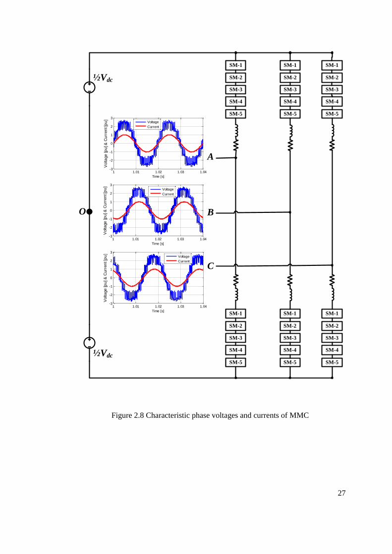
Figure 2.8 Characteristic phase voltages and currents of MMC
28
SM-1
SM-2
SM-3
SM-1
SM-2
O
SM-1
SM-2
SM-3
SM-1
SM-2
SM-1
SM-2
SM-1
SM-2
½VDC
½VDC
B
A
SM-4
SM-5
SM-4
SM-5
SM-3
SM-4
SM-5
SM-3
SM-4
SM-5
SM-3
SM-4
SM-5
SM-3
SM-4
SM-5
C
1 1.005 1.01 1.015 1.02 1.025 1.03 1.035 1.04-5
0
5
Vab
Volt
age
[pu
]
Time [s]1 1.005 1.01 1.015 1.02 1.025 1.03 1.035 1.04
-5
0
5
Vbc V
olt
age
[pu
]
Time [s]
1 1.005 1.01 1.015 1.02 1.025 1.03 1.035 1.04-5
0
5
Vca
Volt
age
[pu
]
Time [s]
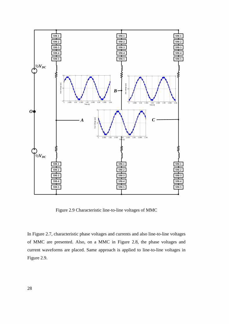
Figure 2.9 Characteristic line-to-line voltages of MMC
In Figure 2.7, characteristic phase voltages and currents and also line-to-line voltages
of MMC are presented. Also, on a MMC in Figure 2.8, the phase voltages and
current waveforms are placed. Same approach is applied to line-to-line voltages in
Figure 2.9.

29
2.3. Analytical Modeling of MMC
Having become familiar to MMC topology and operating principles, analytical
modeling of MMC may be studied. Although the MMC topology seems to have
simple structure, its dynamics and causality relations can be quite complex. There are
several parameters that differently affect the performance in varying conditions.
Therefore, analytical modeling is necessary to understand the nature of the topology
and interpret the results of either simulation or experiment. In addition to this, via
analytical tools, design process such as choosing the arm inductance and submodule
capacitance can be made easier.
In the analysis, it is assumed that all submodule capacitors have the same voltage
variations in time. In this way, considering one capacitor and establishing a model
can be possible. This assumption is reasonable because the capacitor voltage
balancing is necessary in MMC and the proposed methods for the task, detailed in
Section 3.6, are successful. Also, only fundamental-frequency modulating signal is
taken into account as the switching function in order to obtain the characteristics of
the topology. That means this model does not consider pulse-width modulation
(PWM) harmonics which are already reduced and shifted to higher frequencies in
this topology.
In this section, two modeling approaches are detailed. First one is the basic modeling
that broadly models MMC by the differential equations with time-varying
coefficients [23]. Second one targets to extract the relation between the circulating
current and output current. Also, it shows the cyclic relations among the output
current, circulating current, submodule capacitor voltage, and output voltage.

30
2.3.1. Basic Model of MMC
Larm
Rarm
Carm
iU
vU
+
_
vL
+
_
iL
O
½Vdc
½Vdc
iO
Rarm
Larm
icc
Carm
vT
idc
Figure 2.10 Equivalent circuit of MMC used in the modeling
There are N submodules per arm of the MMC. Modulation signal for an ideal
sinusoidal output voltage is given as in Equation (2.1). In this equation, ω is the
output frequency in radian per second and m is modulation index.
(2.1)
(2.2)
31
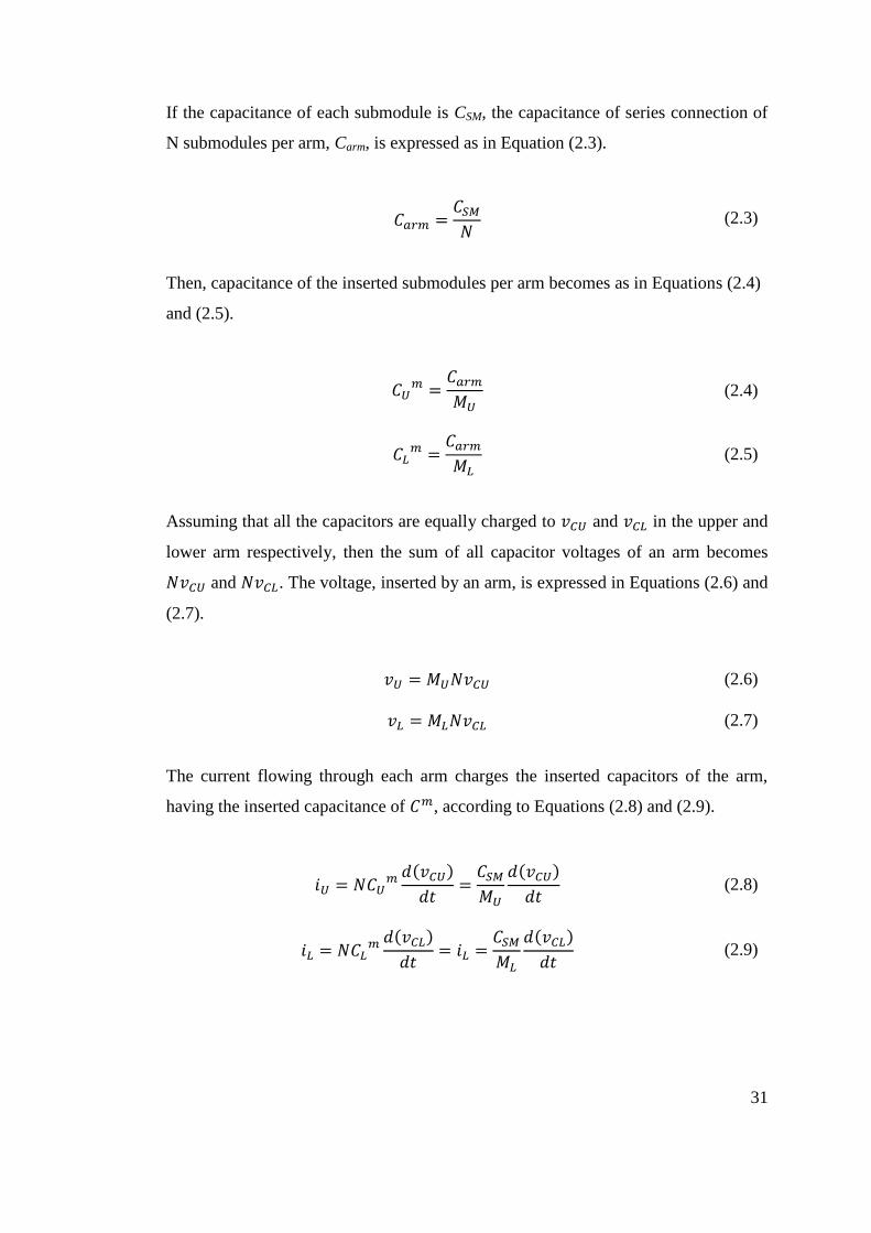
If the capacitance of each submodule is CSM, the capacitance of series connection of
N submodules per arm, Carm, is expressed as in Equation (2.3).
(2.3)
Then, capacitance of the inserted submodules per arm becomes as in Equations (2.4)
and (2.5).
(2.4)
(2.5)
Assuming that all the capacitors are equally charged to and in the upper and
lower arm respectively, then the sum of all capacitor voltages of an arm becomes
and . The voltage, inserted by an arm, is expressed in Equations (2.6) and
(2.7).
(2.6)
(2.7)
The current flowing through each arm charges the inserted capacitors of the arm,
having the inserted capacitance of , according to Equations (2.8) and (2.9).
(2.8)
(2.9)
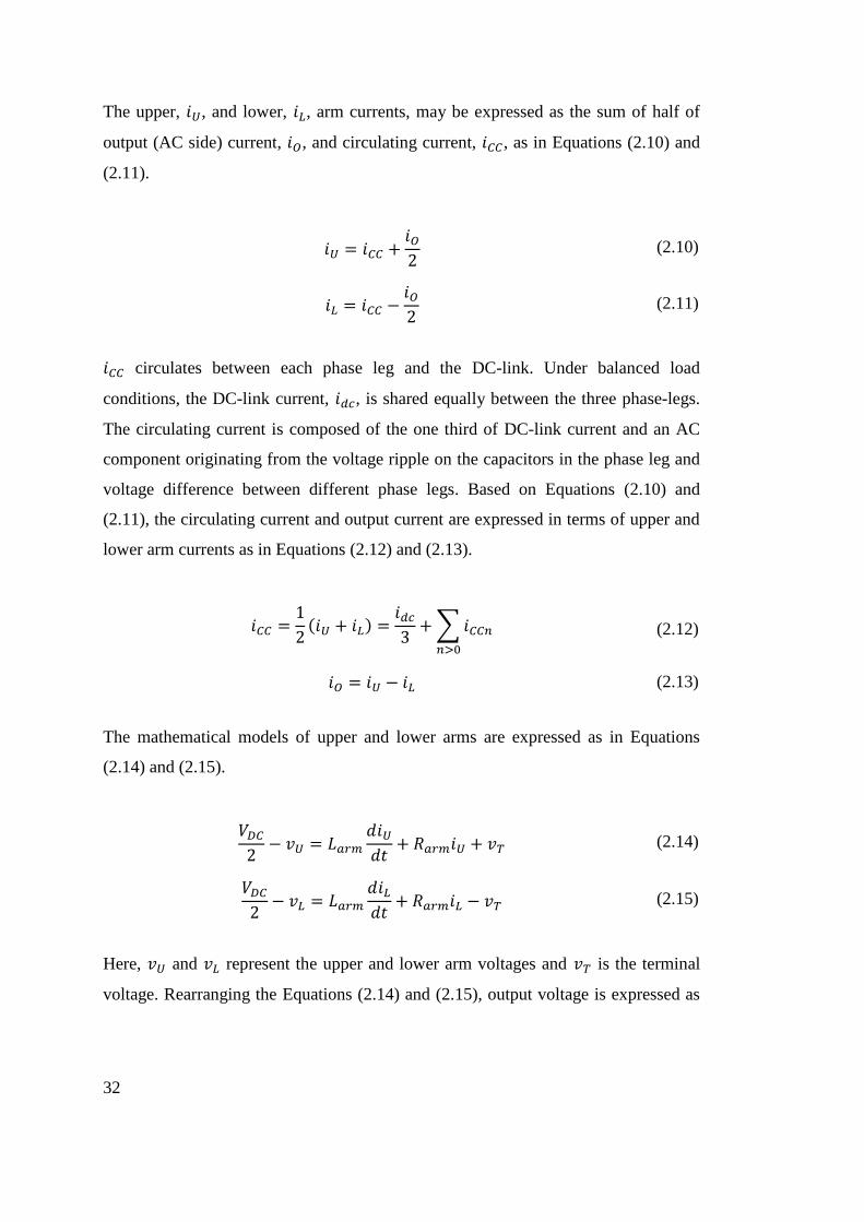
32
The upper, , and lower, , arm currents, may be expressed as the sum of half of
output (AC side) current, , and circulating current, , as in Equations (2.10) and
(2.11).
(2.10)
(2.11)
circulates between each phase leg and the DC-link. Under balanced load
conditions, the DC-link current, , is shared equally between the three phase-legs.
The circulating current is composed of the one third of DC-link current and an AC
component originating from the voltage ripple on the capacitors in the phase leg and
voltage difference between different phase legs. Based on Equations (2.10) and
(2.11), the circulating current and output current are expressed in terms of upper and
lower arm currents as in Equations (2.12) and (2.13).
(2.12)
(2.13)
The mathematical models of upper and lower arms are expressed as in Equations
(2.14) and (2.15).
(2.14)
(2.15)
Here, and represent the upper and lower arm voltages and is the terminal
voltage. Rearranging the Equations (2.14) and (2.15), output voltage is expressed as

33
in Equations (2.16) and (2.17) which constitute the basis for control law in both
output and circulating current.
(2.16)
(2.17)
Circulating current may be written as in Equation (2.18) using Equation (2.6), (2.7),
and (2.17).
(2.18)
Equations (2.8) and (2.9) can be reordered by using and from Equations (2.10)
and (2.11).
(2.19)
(2.20)
Equations (2.19) and (2.20) reveal that the output current affects the voltage balance
of upper and lower arm voltages. Because the steady-state is alternating current,
the time derivative of the upper and lower arm voltages oscillate around a mean
value.
A continuous model of a phase leg is obtained in Equation (2.21) by using Equations
(2.18), (2.19), and (2.20). The state variables are circulating current and one upper
and one lower submodule capacitor voltage.
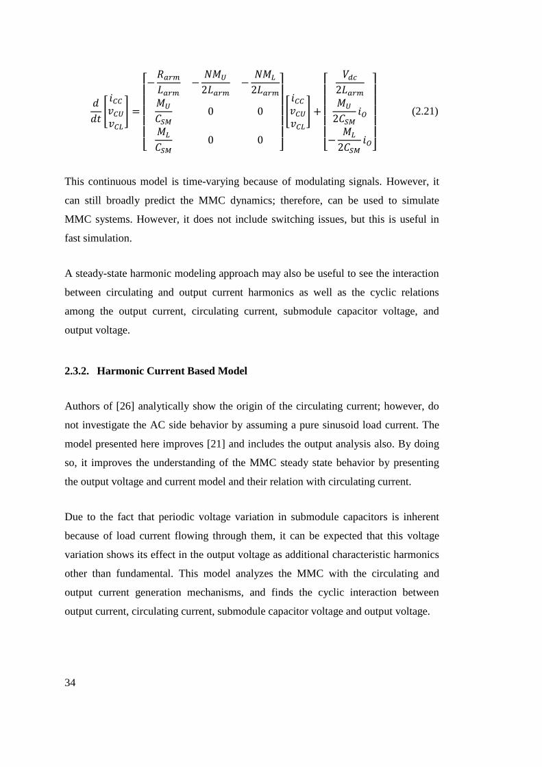
34
(2.21)
This continuous model is time-varying because of modulating signals. However, it
can still broadly predict the MMC dynamics; therefore, can be used to simulate
MMC systems. However, it does not include switching issues, but this is useful in
fast simulation.
A steady-state harmonic modeling approach may also be useful to see the interaction
between circulating and output current harmonics as well as the cyclic relations
among the output current, circulating current, submodule capacitor voltage, and
output voltage.
2.3.2. Harmonic Current Based Model
Authors of [26] analytically show the origin of the circulating current; however, do
not investigate the AC side behavior by assuming a pure sinusoid load current. The
model presented here improves [21] and includes the output analysis also. By doing
so, it improves the understanding of the MMC steady state behavior by presenting
the output voltage and current model and their relation with circulating current.
Due to the fact that periodic voltage variation in submodule capacitors is inherent
because of load current flowing through them, it can be expected that this voltage
variation shows its effect in the output voltage as additional characteristic harmonics
other than fundamental. This model analyzes the MMC with the circulating and
output current generation mechanisms, and finds the cyclic interaction between
output current, circulating current, submodule capacitor voltage and output voltage.

35
2.3.2.1. Basic Definitions
Modulating signals, MU for upper and ML for lower arm, are defined as follows.
(2.22)
(2.23)
In Equations (2.22) and (2.23), m means modulation index and cos(ωt) is the
sinusoidal reference.
The arm currents, for upper and for lower arm, are divided into the two parts,
circulating current and output current components as in Equations (2.24) and
(2.25).
(2.24)
(2.25)
In addition, the arm currents are expressed as sum of harmonics as in Equations
(2.26) and (2.27). For mathematical completeness and calculation simplicity, both
circulating and output current parts begins from the zeroth harmonic (DC term).
(2.26)
(2.27)
where
36
(2.28)
. (2.29)
Submodule capacitor current can be expressed as the multiplication of the
modulating signal and the submodule terminal currents (or equivalently arm
currents) as in Equations (2.30) and (2.31).
(2.30)
(2.31)
By integrating the capacitor currents, the capacitor voltages are found in Equations
(2.32) and (2.33) where CSM means the submodule capacitance as shown in Figure
2.2.
(2.32)
(2.33)
2.3.2.2. Mechanisms of Output and Circulating Current Generation
Having the fundamental definitions, the equations that describe the output and
circulating current generation mechanism can be established.
The upper and lower arm voltages can expressed as the sinusoidal variation of the
total available arm voltages or .
(2.34)
(2.35)

37
The arm voltages expressed in Equations (2.36) and (2.37) are important because the
half of difference of arm voltages, , is the driving voltage of output current and
similarly summation of the arm voltages, , is the voltage that causes the circulating
current.
(2.36)
(2.37)
which can also be written as
(2.38)
(2.39)
It can be seen that both Equations (2.38) and (2.39) include same and
terms with different positions. Using the following
(2.40)
(2.41)
these terms can be written in terms of the arm current parameters as in Equations
(2.42) and (2.43).
(2.42)
38
(2.43)
whose integrals are given as follows.
(2.44)
(2.45)
The first order terms of time in Equations (2.44) and (2.45) should cancel out;
otherwise, they grow as time passes, resulting illogically high values. As a result,
Equations (2.46) and (2.47) should be satisfied in a working MMC.
(2.46)
(2.47)
39
Integration constants of Equations (2.44) and (2.45) represent average charge. Notice
that it is assumed that all capacitors in both upper and lower arm have same steady
state average charge where is the capacitor average (DC) voltage.
Therefore, by sum operation, Equation (2.44) will have the constant term as
average charge while Equation (2.45) will have a zero constant term because two
integrands cancel out their equal constant terms by subtraction operation.
By substituting Equations (2.44) and (2.45) into Equations (2.38) and (2.39), and
can be written as follows.
(2.48)
40
(2.49)
To simplify the calculations, the complex number representation of the currents and
voltages can be used. All currents and voltages are then re-arranged by using the
structure shown in Equations (2.50) and (2.51).
(2.50)
. (2.51)
Having the complex form, it is easy to separate the variables and to put Equations
(2.48) and (2.49) into matrix structure. Note that double stressed letters represent
matrices.
41
(2.52)
(2.53)
where
(2.54)
(2.55)
(2.56)
(2.57)
(2.58)
(2.59)
42
(2.60)
(2.61)
(2.62)
(2.63)
(2.64)
(2.65)
(2.66)
(2.67)
(2.68)
Note that form is same as . The matrix separates the “ ”
information of Equations (2.48) and (2.49) leaving the time-invariant parameters
together.
Equations (2.52) and (2.53) can be represented in a more compact way as follows.
(2.69)
43
(2.70)
where
(2.71)
(2.72)
Notice that new matrix with the elements of and matrix with the
elements of and are defined. Also, matrix is common both sides of
Equations (2.69) and (2.70) leading to its cancelation.
As an interesting point, MMC generates characteristic odd-harmonic voltages in
addition to the fundamental component although the modulating signal is pure
sinusoid. Dominant one seems to be third harmonic. This result can be understood by
looking at Equations (2.52) and (2.53). The -harmonic generated output voltage is
affected by , and harmonic output currents and
and harmonic circulating currents. For example, it can be said that third-
harmonic generated output voltage is due to mainly first- and fifth-harmonic output
current and mainly second- and fourth-harmonic circulating currents. The output
harmonic-voltages other than fundamental are generated as a side effect due to the
converter nature. Their magnitudes depend proportionally on the output current and
inversely on the submodule capacitance. The generated third-harmonic voltage is
expected to be biggest characteristic harmonic voltage because its generation is
heavily affected by the fundamental-frequency current. However, in a balanced
three-wire three-phase system, this voltage cannot force a current because the third

44
harmonic is a zero sequence harmonic. In this way, the generation of the remaining
odd harmonics is also limited because of zero third-harmonic output current.
Similar interpretation can be applied to the harmonic arm voltage summation in
Equation (2.53) that drives the circulating current. The dominating circulating
current, second harmonic, is shaped by mainly fundamental-frequency output current
and mainly DC, second-, and fourth-harmonic circulating current.
This model, by analyzing the MMC with two main dynamics, circulating and output
current generation mechanism, obtained the direct relation between these currents
and showed that the two current cannot be thought separately. Output voltage
generation is discussed and shown to be a function of these currents. This work also
points out the characteristics odd harmonics in the output voltage. Basically it is the
reflection of capacitor voltage variation.
2.4. MMC Design
Converter hardware design and component sizing of MMC is an involved procedure.
In an MMC, the number of submodules per arm, the power semiconductor electrical
ratings, the arm inductor and submodule capacitor value should be determined.
Designing of all these may be dependent on each other. In this section, basic
directions in the design of are provided.
In Figure 2.11, an MMC design flow is provided. First, MMC power level is needed.
According to the power level of proposed MMC, the DC-link voltage is chosen
considering the standard voltage and current ratings of the components. Then,
depending on the target voltage waveform quality and available semiconductor
ratings, the submodules per arm, N, is determined. Here, semiconductors are also
chosen. Next, passive components are selected. The submodule capacitance is
typically chosen to achieve low voltage ripple in operation. The arm inductance is
45
also needed to isolate the upper and lower arm and to limit circulating current. These
steps are detailed below.
System Power, S
DC-link Voltage,
Vdc
Submodules per
Arm, N
Submodule
Capacitance, CSM
Arm Inductance,
Larm
Figure 2.11 MMC design order
2.4.1. Determining the Number of Submodules per Arm
The number of submodules per arm, N, is among fundamental parameters of the
MMC topology to be determined. The ease of scalability and adaptability to different
voltage and power levels is one of the advantages of MMC over conventional VSCs.
Here, design of the submodule number per arm, N, plays central role. As N increased,
higher voltage and power can be handled.
When determining the number of submodules per arm, N, two basic design values
are important. First one is the DC-link voltage because the DC-link voltage is
distributed evenly to N submodules in an arm. Therefore, the average voltage on a
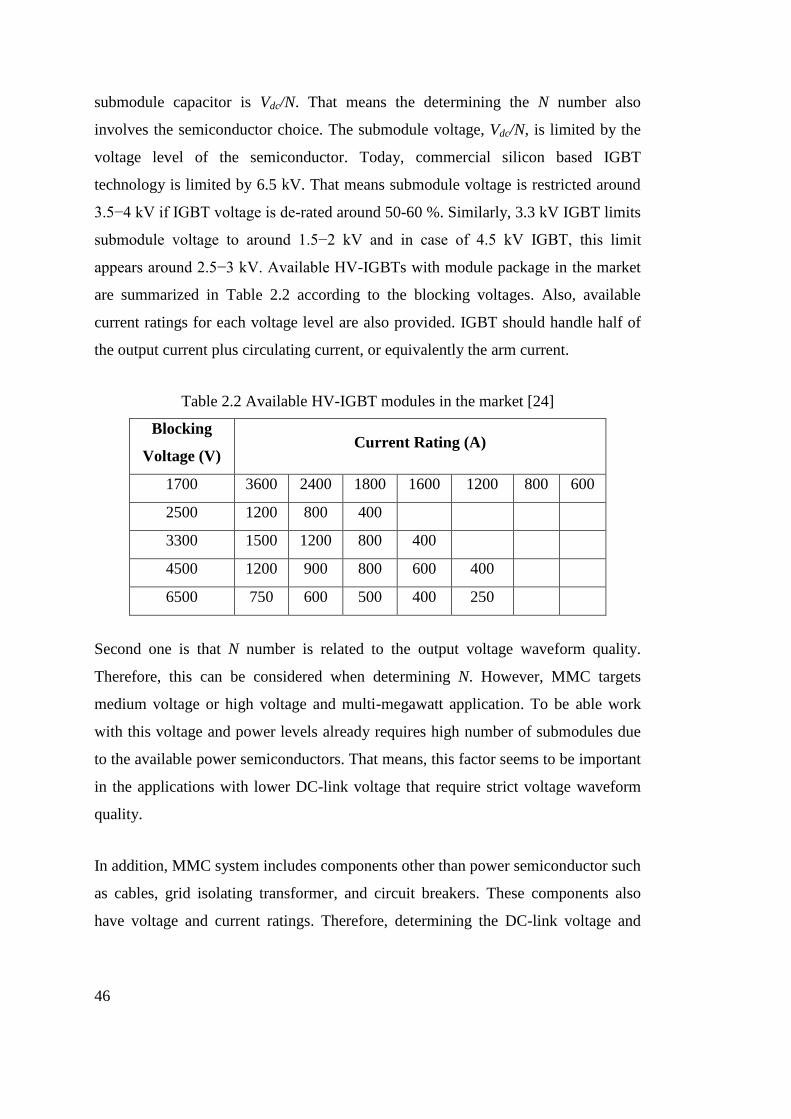
46
submodule capacitor is Vdc/N. That means the determining the N number also
involves the semiconductor choice. The submodule voltage, Vdc/N, is limited by the
voltage level of the semiconductor. Today, commercial silicon based IGBT
technology is limited by 6.5 kV. That means submodule voltage is restricted around
3.5−4 kV if IGBT voltage is de-rated around 50-60 %. Similarly, 3.3 kV IGBT limits
submodule voltage to around 1.5−2 kV and in case of 4.5 kV IGBT, this limit
appears around 2.5−3 kV. Available HV-IGBTs with module package in the market
are summarized in Table 2.2 according to the blocking voltages. Also, available
current ratings for each voltage level are also provided. IGBT should handle half of
the output current plus circulating current, or equivalently the arm current.
Table 2.2 Available HV-IGBT modules in the market [24]
Blocking
Voltage (V) Current Rating (A)
1700 3600 2400 1800 1600 1200 800 600
2500 1200 800 400
3300 1500 1200 800 400
4500 1200 900 800 600 400
6500 750 600 500 400 250
Second one is that N number is related to the output voltage waveform quality.
Therefore, this can be considered when determining N. However, MMC targets
medium voltage or high voltage and multi-megawatt application. To be able work
with this voltage and power levels already requires high number of submodules due
to the available power semiconductors. That means, this factor seems to be important
in the applications with lower DC-link voltage that require strict voltage waveform
quality.
In addition, MMC system includes components other than power semiconductor such
as cables, grid isolating transformer, and circuit breakers. These components also
have voltage and current ratings. Therefore, determining the DC-link voltage and
47
output current values of MMC to reach the desired power level may also be restricted
by these components and, of course, system cost.
After determining DC-link voltage by system design perspective and then submodule
voltage, VSM, considering available IGBT ratings, the expression in Equation (2.73)
may be utilized to determine N.
(2.73)
As a last remark, redundant submodule should also be considered. After failure of a
submodule, the damaged submodule may be isolated from the system and then, in
place the damaged one, a redundant submodule may be substituted. Therefore, a few
redundant submodules may also be added to improve system reliability.
2.4.2. Sizing of the Submodule Capacitor
Submodule capacitor requires consideration on the acceptable capacitor voltage
ripple. As it is said before, capacitors are floating and are charged and discharged by
arm currents. Therefore, arm current causes unavoidable voltage ripple which is
inversely related to the capacitance. Voltage ripple cannot be totally eliminated, but
its magnitude can be lowered by choosing submodule capacitance reasonably.
Arbitrarily high capacitance may be unnecessary and expensive. In addition,
eliminating the harmonics in the circulating current may also help limiting the
capacitor voltage ripple.
A voltage ripple magnitude based capacitor dimensioning is proposed in [25] and
given in Equation (2.74). Here, S means apparent power and is the power
factor. Average capacitor voltage is and is the ripple percentage.

48
(2.74)
In the literature, approximately 10 % voltage ripple of submodule capacitors is
considered suitable [26].
Another approach may be the use of the stored energy (EC) in the all submodule
capacitors of the total system which is given in Equation (2.75).
(2.75)
To ease the comparison between different systems and bring some abstraction, a new
concept, energy-power ratio (EP), is defined in Equation (2.76).
(2.76)
Combining Equations (2.75) and (2.76), the submodule capacitance can be written in
terms of power, DC-link voltage, N, and energy-power ratio as in Equation (2.77).
With a specific design, capacitance can be adjusted using energy-power ratio now.
(2.77)
Energy-power ratio is kept in a range of 30 kJ/MVA to 40 kJ/kVA, depending on the
application and converter [26]. Indeed, Siemens uses 30 kJ/MVA energy-power
ratio, equivalent to 10-mF submodule capacitance, in its INELFE project, a 1000
MW HVDC system between France and Spain [27]. This value satisfies the
condition given in Equation (2.74) with the rule of maximum 10 % voltage ripple if
taking m and as one.
49
Apart from capacitance value, capacitor ripple current capability, voltage rating, and
reliability issues such as hot-spot temperature, FIT rate, and life time should also be
considered.
2.4.3. Sizing of the Arm Inductor
Arm (buffer) inductor is connected in series with the submodules, and used to isolate
upper and lower arm. In this way, it also limits the circulating current. In addition,
output current is also filtered by the arm inductor as this current should flow through
the arm inductor. However, equivalent inductance due to arm inductor seen by the
output current is half of the arm inductance as it can be understood from Equation
(2.16). On the other hand, the effective inductance for circulating current is two
times the arm inductance as the Equation (2.17) shows.
In [21], a new concept of natural resonance frequencies of the converter is
introduced. The submodule capacitance and arm inductance forms a resonance
frequency for the converter. Equation (2.78) gives the values of resonance
frequencies where n is the harmonic number, n=3k±1.
(2.78)
If the converter is operated at the resonant frequency, ωr, then the nth
harmonic
current is only limited by the arm resistance, which is deliberately kept small for
higher efficiency. Therefore, it is advised to operate the converter above the highest
resonant frequency, which occurs with n=2 and m=1. Substituting these, Equation
(2.78) may be written as follows.
(2.79)
50
Then, the following Equation (2.79), a restriction is found in Equation (2.80) for the
arm inductance and submodule capacitance whose multiplication should have a
minimum value depending on submodule number per arm, N, and operating
frequency, ω.
(2.80)
Apart from the resonance frequency phenomenon, in case of DC-link short circuit,
the arm inductors will limit the fault current. Therefore, it may also be taken into
consideration [28].
As a practical example, Siemens uses 50-mH arm inductor in the INELFE project
which is equivalent to 0.15 pu [26]. This value satisfies the condition given in
Equation (2.80) considering that the project uses 10-mF submodule capacitance and
400 submodules per arm.
2.5. Summary
In this chapter, at first, the basic structure of MMC is discussed. The definitions and
illustrations of MMC are provided. Second, basically how the converter works is
studied with detailed visual descriptions which progressively develop from
submodule level to leg and then to terminal voltage levels. The structure and working
principles are described with comparisons with basic converters such as 2L-VSCs.
Third, the modeling approaches of MMC are presented. The basic model seeks the
differential equations that broadly show the inner dynamics of MMC. Another model
is developed on the harmonic content of the circulating and output current. This is
used to show the cyclic relation among the submodule capacitance voltage, output
voltage, output current, and circulating current. At last, basic design directions for
MMC are provided. Selection of N number is discussed in conjunction with
semiconductor choice and DC-link voltage as well as redundant submodules for
51
increased reliability. Sizing of submodule capacitance is related to voltage ripple. A
convenient approach using energy-power ratio concept and its practical values from
field applications are discussed. Sizing of arm inductance is related to limiting
circulating current. Furthermore, intrinsic resonant frequencies, created by the arm
inductance and the submodule capacitance, should be lower than the operating
frequency.

52
53
CHAPTER 3
3. CONTROL OF MODULAR MULTILEVEL CONVERTER
CONTROL OF MODULAR MULTILEVEL CONVERTER
3.1. Introduction
Control theory works with the dynamic systems and modifies their behaviors by an
external controller. The aim of the control theory is to make a system to follow a
desired reference signal. In power electronics, generally inductor current, capacitor
voltage and motor speed is controlled. Their basic electrical and mechanical
equations that describe the dynamics determine the controlled variable and control
action to be utilized.
Switching and control issues of MMC are similar to the conventional 2L-VSCs.
Output current, DC-link voltage, and active and reactive power control methods are
fundamentally the same as the 2L-VSCs. However, it has some unique aspects also.
The fact that MMC has floating capacitors is the main reason for the extra control
requirement. The major control difference lies in the capacitor voltage balancing. If
this is not successfully handled, the MMC perhaps loses stability and cannot operate.
Additionally, the presence of the circulating current leads to another control, the
suppression of harmonic content of circulating current. In this way, efficiency
improvement in the converter and usage of components with low ratings may be
possible. Furthermore, in the literature, several types of PWM methods for MMC are
proposed.

54
Apart from output current, DC-link voltage, and power control, which are
fundamentally common to all VSCs, in the literature, there are mainly two types of
inner control which deals with the special control aspects of MMC. First one is based
on sorting algorithm and proposed by Lesnicar and Marquardt in [6] and [29]. The
other one is based on phase-shifted PWM and proposed by Hagiwara and Akagi in
[30]. Although first method will be detailed and utilized in this thesis, second method
will also be briefly explained.
In Figure 3.1, a general control diagram based on the sorting algorithm is presented.
It summarizes all parts of the MMC control, including output current control, DC-
link voltage control, and power control as well as circulating current control, PWM,
and sorting algorithm.
– /+
VDC /2
Vo_ctrl*
Vcc_ctrl*
+
PWM
Gate
SignalsSORTING
ALGORITHM
NonVU/L*OUTPUT
CURRENT
CONTROL
CIRCULATING
CURRENT
CONTROL
–
Seperate for each arm
Icc*
MMC
PLLθe & ωe
VSMIo
IU/L
Current
FeedbackIo
POWER
and/or
DC-LINK
VOLTAGE
CONTROL
Icc
Icc
VDC*
Io*
Iarm
P*
Q*
VDC P Q
Figure 3.1 Block diagram of sorting algorithm based control approach
The target DC-link voltage and output power are the primary reference for the whole
system. DC-link voltage and output power controller generate the output current
reference to keep the voltage or power reference and feedback value matched. Then,
output current controller produces the necessary output voltage reference that allows
the current to flow as desired. These are similar to conventional control approaches
employed in 2L-VSCs. Circulating current controller, on the other hand, produces
55
the required voltage value to suppress the second-harmonic circulating current and it
works in parallel to the output current controller. Using the output voltage reference
from output current controller and the voltage reference from circulating current
controller as well as the offset of , the arm voltage reference is obtained for
each arm separately. Then, the inserted submodule number per arm, Non, is found by
using the PWM operation of the arm voltage reference. Notice that PWM is not
responsible from generating gate signals for semiconductors. Sorting algorithm uses
Non, arm current direction and all submodule voltages in the arm to generate gate
signals. By doing so, it guarantees the voltage balancing among the submodule
capacitors in the arm. These are also summarized in [31] and [32].
In this chapter, the output current control is discussed first. The derivation of the
current controller, vector control concept, the detailed structure of the current
controller, and controller tuning method are presented. Subsequently, DC-link
voltage control is studied. Again, the controller is derived step by step and the whole
control structure is presented. A tuning method for DC-link voltage controller is also
provided. Later, power controller is discussed. Furthermore, the modulation methods
suitable for MMC are viewed. Using carrier based modulation, N+1 and 2N+1 level
voltage generation methods are shown. Also, an appropriate modulation technique
for the MMC designs with the high number of submodules per arm is mentioned.
This method is named as nearest level modulation. Lastly, inner control of MMC,
including circulating current control and capacitor voltage balancing, is studied by
citing the two main approaches to accomplish these tasks.
3.2. Output Current Control
3.2.1. Current Control Basics
Current control is generally related to the current of inductor. The electrical equation
of inductor is
where VL and iL are the inductor voltage and current,
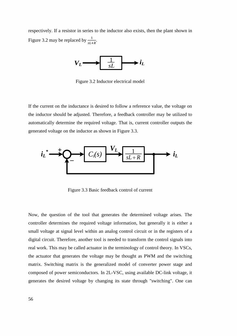
56
respectively. If a resistor in series to the inductor also exists, then the plant shown in
Figure 3.2 may be replaced by
.
iLVL sL1
Figure 3.2 Inductor electrical model
If the current on the inductance is desired to follow a reference value, the voltage on
the inductor should be adjusted. Therefore, a feedback controller may be utilized to
automatically determine the required voltage. That is, current controller outputs the
generated voltage on the inductor as shown in Figure 3.3.
+
_Ci(s)iL
*iL
VL
RsL 1
Figure 3.3 Basic feedback control of current
Now, the question of the tool that generates the determined voltage arises. The
controller determines the required voltage information, but generally it is either a
small voltage at signal level within an analog control circuit or in the registers of a
digital circuit. Therefore, another tool is needed to transform the control signals into
real work. This may be called actuator in the terminology of control theory. In VSCs,
the actuator that generates the voltage may be thought as PWM and the switching
matrix. Switching matrix is the generalized model of converter power stage and
composed of power semiconductors. In 2L-VSC, using available DC-link voltage, it
generates the desired voltage by changing its state through "switching". One can
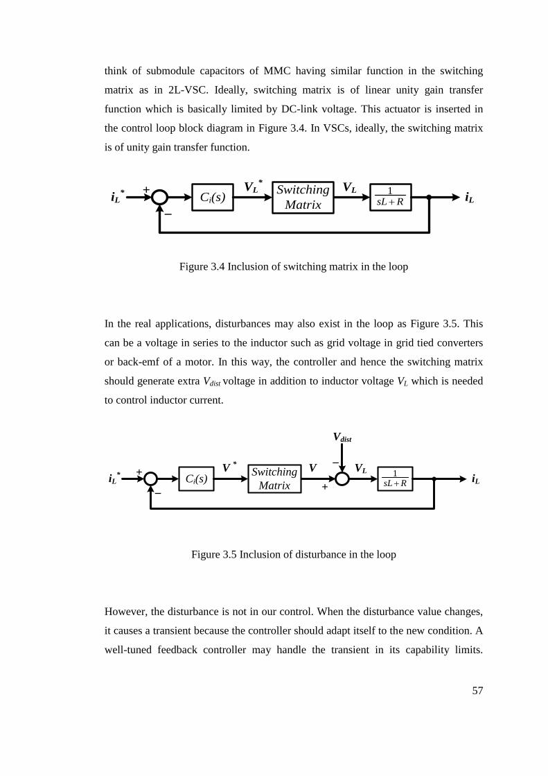
57
think of submodule capacitors of MMC having similar function in the switching
matrix as in 2L-VSC. Ideally, switching matrix is of linear unity gain transfer
function which is basically limited by DC-link voltage. This actuator is inserted in
the control loop block diagram in Figure 3.4. In VSCs, ideally, the switching matrix
is of unity gain transfer function.
+
_Ci(s)iL
*iL
VLVL*
Switching
Matrix RsL 1
Figure 3.4 Inclusion of switching matrix in the loop
In the real applications, disturbances may also exist in the loop as Figure 3.5. This
can be a voltage in series to the inductor such as grid voltage in grid tied converters
or back-emf of a motor. In this way, the controller and hence the switching matrix
should generate extra Vdist voltage in addition to inductor voltage VL which is needed
to control inductor current.
+
_Ci(s)iL
*iL
VLV *
V
Vdist
+
_
RsL 1Switching
Matrix
Figure 3.5 Inclusion of disturbance in the loop
However, the disturbance is not in our control. When the disturbance value changes,
it causes a transient because the controller should adapt itself to the new condition. A
well-tuned feedback controller may handle the transient in its capability limits.
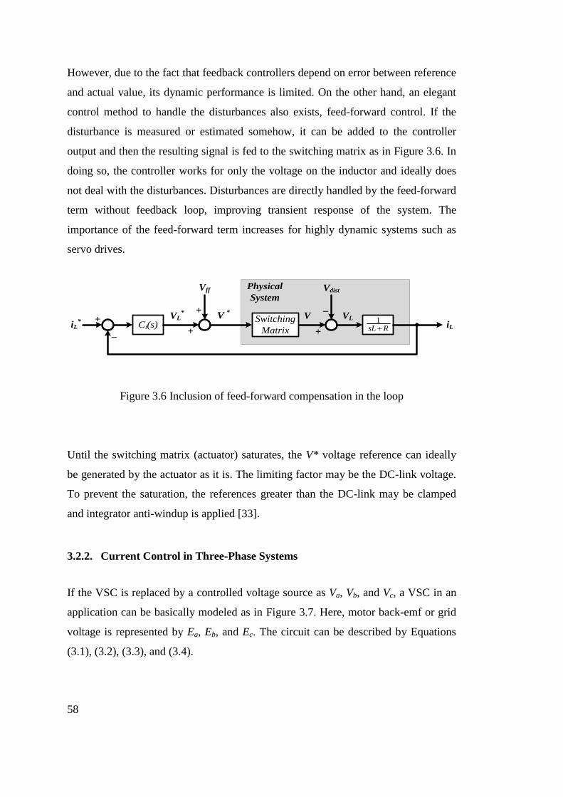
58
However, due to the fact that feedback controllers depend on error between reference
and actual value, its dynamic performance is limited. On the other hand, an elegant
control method to handle the disturbances also exists, feed-forward control. If the
disturbance is measured or estimated somehow, it can be added to the controller
output and then the resulting signal is fed to the switching matrix as in Figure 3.6. In
doing so, the controller works for only the voltage on the inductor and ideally does
not deal with the disturbances. Disturbances are directly handled by the feed-forward
term without feedback loop, improving transient response of the system. The
importance of the feed-forward term increases for highly dynamic systems such as
servo drives.
+
_Ci(s)iL
*iL
VLVL*
V
Vdist
+
_
+
+V
*
Vff
RsL 1
Physical
System
Switching
Matrix
Figure 3.6 Inclusion of feed-forward compensation in the loop
Until the switching matrix (actuator) saturates, the V* voltage reference can ideally
be generated by the actuator as it is. The limiting factor may be the DC-link voltage.
To prevent the saturation, the references greater than the DC-link may be clamped
and integrator anti-windup is applied [33].
3.2.2. Current Control in Three-Phase Systems
If the VSC is replaced by a controlled voltage source as Va, Vb, and Vc, a VSC in an
application can be basically modeled as in Figure 3.7. Here, motor back-emf or grid
voltage is represented by Ea, Eb, and Ec. The circuit can be described by Equations
(3.1), (3.2), (3.3), and (3.4).
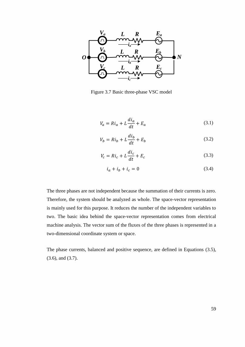
59
R EaL
R EbL
R EcL
Va
Vb
Vc
O N
ic
ia
ib
Figure 3.7 Basic three-phase VSC model
(3.1)
(3.2)
(3.3)
(3.4)
The three phases are not independent because the summation of their currents is zero.
Therefore, the system should be analyzed as whole. The space-vector representation
is mainly used for this purpose. It reduces the number of the independent variables to
two. The basic idea behind the space-vector representation comes from electrical
machine analysis. The vector sum of the fluxes of the three phases is represented in a
two-dimensional coordinate system or space.
The phase currents, balanced and positive sequence, are defined in Equations (3.5),
(3.6), and (3.7).
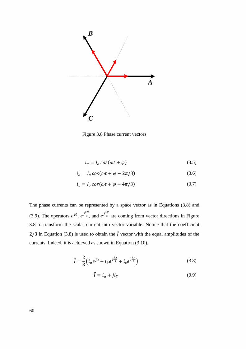
60
A
C
B
Figure 3.8 Phase current vectors
(3.5)
(3.6)
(3.7)
The phase currents can be represented by a space vector as in Equations (3.8) and
(3.9). The operators ,
, and
are coming from vector directions in Figure
3.8 to transform the scalar current into vector variable. Notice that the coefficient
in Equation (3.8) is used to obtain the vector with the equal amplitudes of the
currents. Indeed, it is achieved as shown in Equation (3.10).
(3.8)
(3.9)
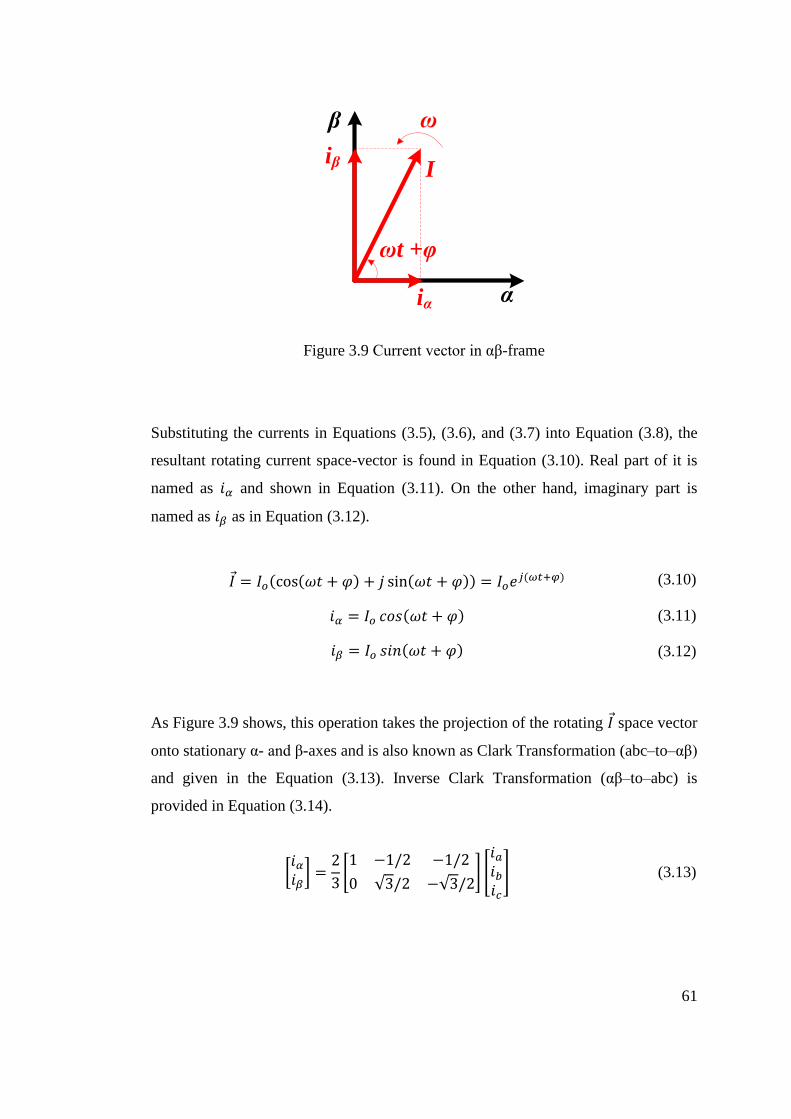
61
α
β ω
I
iα
iβ
ωt +φ
Figure 3.9 Current vector in αβ-frame
Substituting the currents in Equations (3.5), (3.6), and (3.7) into Equation (3.8), the
resultant rotating current space-vector is found in Equation (3.10). Real part of it is
named as and shown in Equation (3.11). On the other hand, imaginary part is
named as as in Equation (3.12).
(3.10)
(3.11)
(3.12)
As Figure 3.9 shows, this operation takes the projection of the rotating space vector
onto stationary α- and β-axes and is also known as Clark Transformation (abc–to–αβ)
and given in the Equation (3.13). Inverse Clark Transformation (αβ–to–abc) is
provided in Equation (3.14).
(3.13)
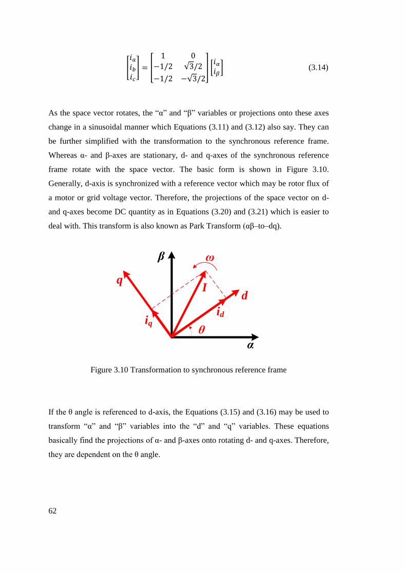
62
(3.14)
As the space vector rotates, the “α” and “β” variables or projections onto these axes
change in a sinusoidal manner which Equations (3.11) and (3.12) also say. They can
be further simplified with the transformation to the synchronous reference frame.
Whereas α- and β-axes are stationary, d- and q-axes of the synchronous reference
frame rotate with the space vector. The basic form is shown in Figure 3.10.
Generally, d-axis is synchronized with a reference vector which may be rotor flux of
a motor or grid voltage vector. Therefore, the projections of the space vector on d-
and q-axes become DC quantity as in Equations (3.20) and (3.21) which is easier to
deal with. This transform is also known as Park Transform (αβ–to–dq).
α
β
q
d
ω
θ
I
iq id
Figure 3.10 Transformation to synchronous reference frame
If the θ angle is referenced to d-axis, the Equations (3.15) and (3.16) may be used to
transform “α” and “β” variables into the “d” and “q” variables. These equations
basically find the projections of α- and β-axes onto rotating d- and q-axes. Therefore,
they are dependent on the θ angle.
63
(3.15)
(3.16)
Equations (3.15) and (3.16) representing Park Transform can be written in a matrix
form as in Equations (3.17). Inverse Park Transform is given in Equation (3.18).
(3.17)
(3.18)
In fact, Park Transform is equivalent to multiplying Equation (3.10) with . If
θ=ωt is assumed, then Equations (3.19), (3.20), and (3.21) are obtained. The Inverse
Park Transform (dq-to-αβ) is also equivalent to multiplying Equation (3.19) with
.
(3.19)
(3.20)
(3.21)
Direct transformation from abc-frame to dq-frame (abc–to–dq) may be done as
Equation (3.22) shows.
(3.22)
Transformation matrix from abc-frame to dq-frame is given by Equation (3.23). The
inverse of this operation is also provided in Equation (3.24).
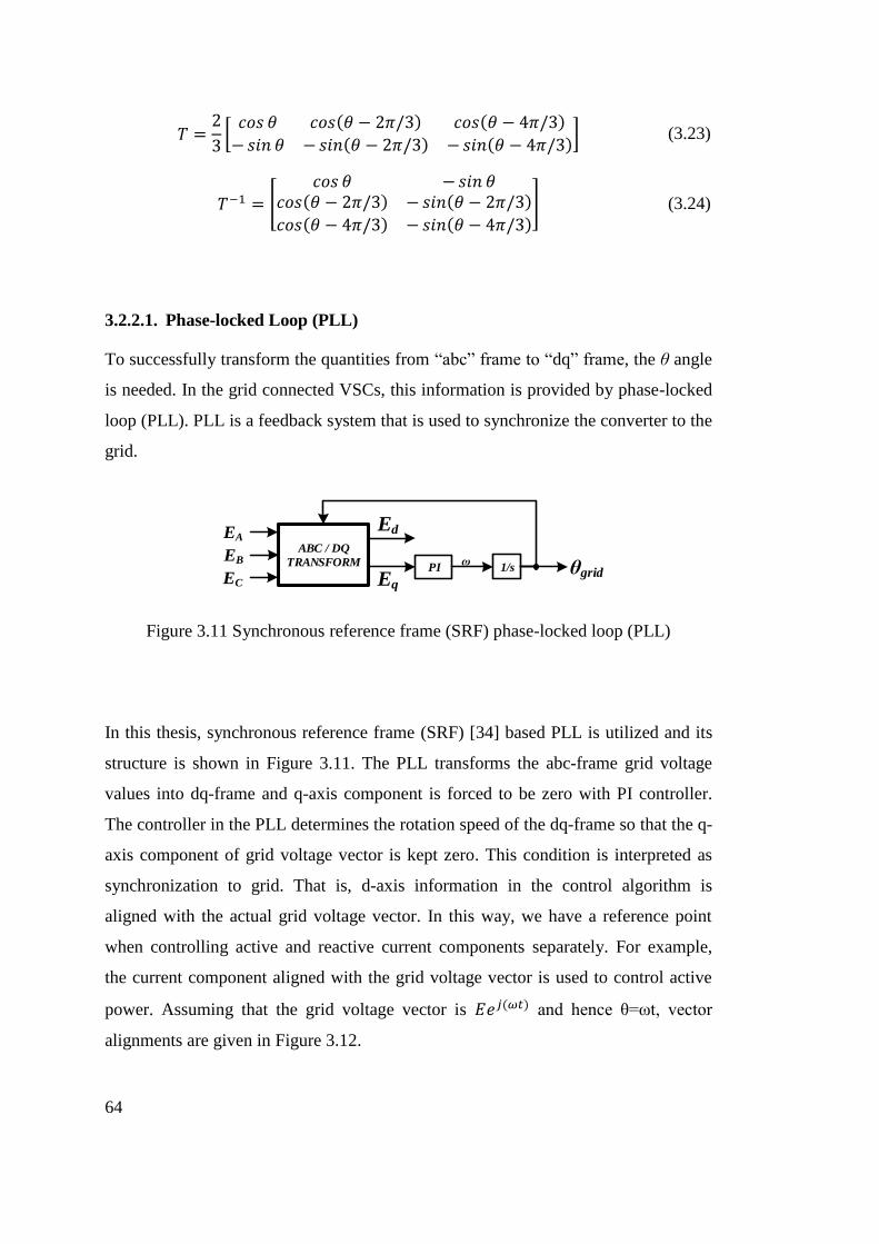
64
(3.23)
(3.24)
3.2.2.1. Phase-locked Loop (PLL)
To successfully transform the quantities from “abc” frame to “dq” frame, the θ angle
is needed. In the grid connected VSCs, this information is provided by phase-locked
loop (PLL). PLL is a feedback system that is used to synchronize the converter to the
grid.
PI
Eqθgrid
EA
EB
EC
ABC / DQ
TRANSFORM
Ed
1/sω
Figure 3.11 Synchronous reference frame (SRF) phase-locked loop (PLL)
In this thesis, synchronous reference frame (SRF) [34] based PLL is utilized and its
structure is shown in Figure 3.11. The PLL transforms the abc-frame grid voltage
values into dq-frame and q-axis component is forced to be zero with PI controller.
The controller in the PLL determines the rotation speed of the dq-frame so that the q-
axis component of grid voltage vector is kept zero. This condition is interpreted as
synchronization to grid. That is, d-axis information in the control algorithm is
aligned with the actual grid voltage vector. In this way, we have a reference point
when controlling active and reactive current components separately. For example,
the current component aligned with the grid voltage vector is used to control active
power. Assuming that the grid voltage vector is and hence θ=ωt, vector
alignments are given in Figure 3.12.
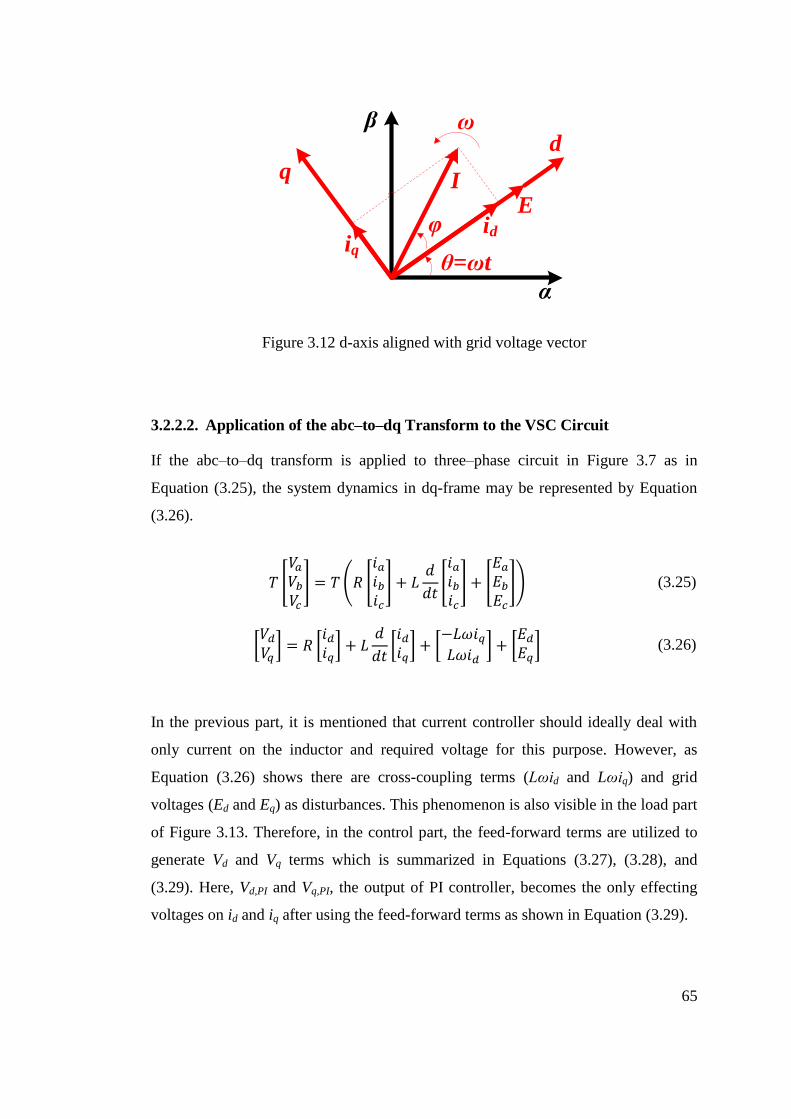
65
q
α
β d
ω
θ=ωt
IE
φiq
id
Figure 3.12 d-axis aligned with grid voltage vector
3.2.2.2. Application of the abc–to–dq Transform to the VSC Circuit
If the abc–to–dq transform is applied to three–phase circuit in Figure 3.7 as in
Equation (3.25), the system dynamics in dq-frame may be represented by Equation
(3.26).
(3.25)
(3.26)
In the previous part, it is mentioned that current controller should ideally deal with
only current on the inductor and required voltage for this purpose. However, as
Equation (3.26) shows there are cross-coupling terms (Lωid and Lωiq) and grid
voltages (Ed and Eq) as disturbances. This phenomenon is also visible in the load part
of Figure 3.13. Therefore, in the control part, the feed-forward terms are utilized to
generate Vd and Vq terms which is summarized in Equations (3.27), (3.28), and
(3.29). Here, Vd,PI and Vq,PI, the output of PI controller, becomes the only effecting
voltages on id and iq after using the feed-forward terms as shown in Equation (3.29).
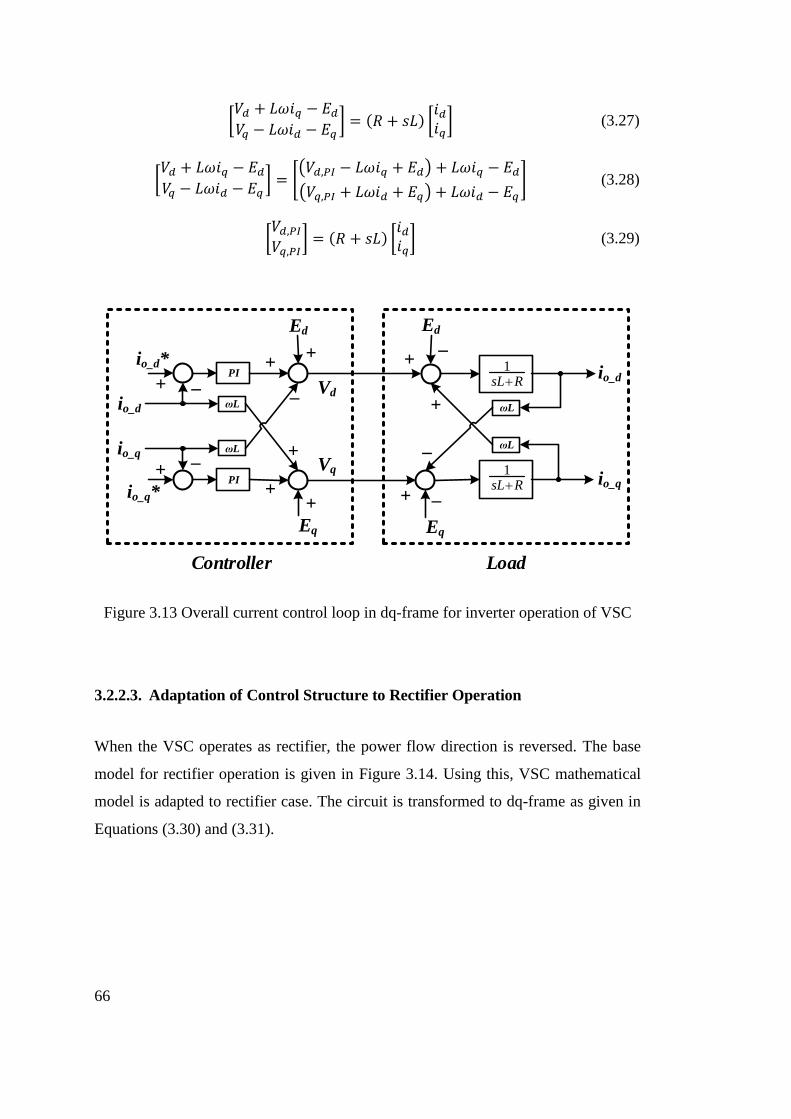
66
(3.27)
(3.28)
(3.29)
io_q*+
+ _
_
PI
PI
io_q
io_d*
Eq
Ed
ωL
ωL
+
io_d
+
++
_
+
1sL R
Ed
_
1sL R
ωL
ωL
_
Eq
io_d
io_q
+
_
+
+
Controller Load
Vd
Vq
Figure 3.13 Overall current control loop in dq-frame for inverter operation of VSC
3.2.2.3. Adaptation of Control Structure to Rectifier Operation
When the VSC operates as rectifier, the power flow direction is reversed. The base
model for rectifier operation is given in Figure 3.14. Using this, VSC mathematical
model is adapted to rectifier case. The circuit is transformed to dq-frame as given in
Equations (3.30) and (3.31).
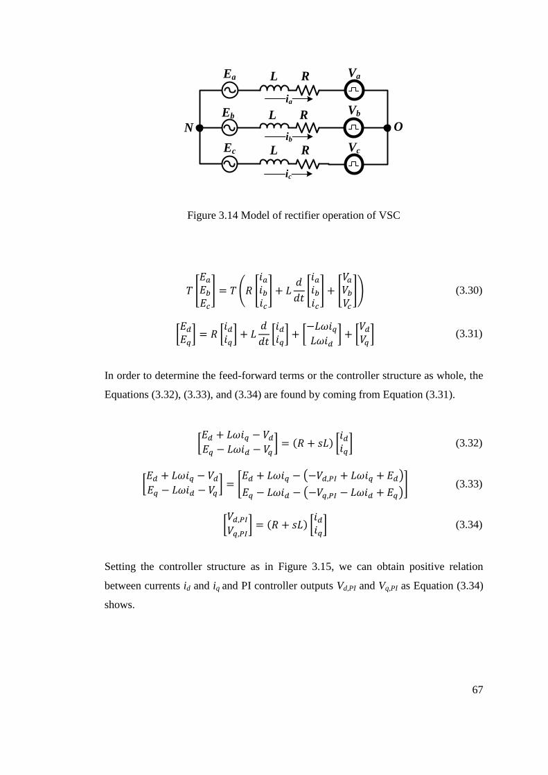
67
O
RL
RL
RL
N
ic
ia
ib
Va
Vb
Vc
Ea
Eb
Ec
Figure 3.14 Model of rectifier operation of VSC
(3.30)
(3.31)
In order to determine the feed-forward terms or the controller structure as whole, the
Equations (3.32), (3.33), and (3.34) are found by coming from Equation (3.31).
(3.32)
(3.33)
(3.34)
Setting the controller structure as in Figure 3.15, we can obtain positive relation
between currents id and iq and PI controller outputs Vd,PI and Vq,PI as Equation (3.34)
shows.
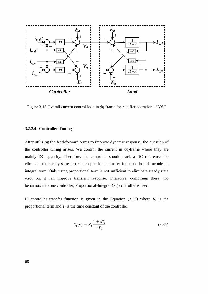
68
io_q*+
+ _
_
PI
PI
io_q
io_d*
Eq
Ed
ωL
ωL
+
io_d
_
_ +
+
_
1sL R
Ed
1sL R
ωL
ωL
+Eq
io_d
io_q
_
+
_
_
Controller Load
Vd
Vq
+
Figure 3.15 Overall current control loop in dq-frame for rectifier operation of VSC
3.2.2.4. Controller Tuning
After utilizing the feed-forward terms to improve dynamic response, the question of
the controller tuning arises. We control the current in dq-frame where they are
mainly DC quantity. Therefore, the controller should track a DC reference. To
eliminate the steady-state error, the open loop transfer function should include an
integral term. Only using proportional term is not sufficient to eliminate steady state
error but it can improve transient response. Therefore, combining these two
behaviors into one controller, Proportional-Integral (PI) controller is used.
PI controller transfer function is given in the Equation (3.35) where Ki is the
proportional term and Ti is the time constant of the controller.
(3.35)
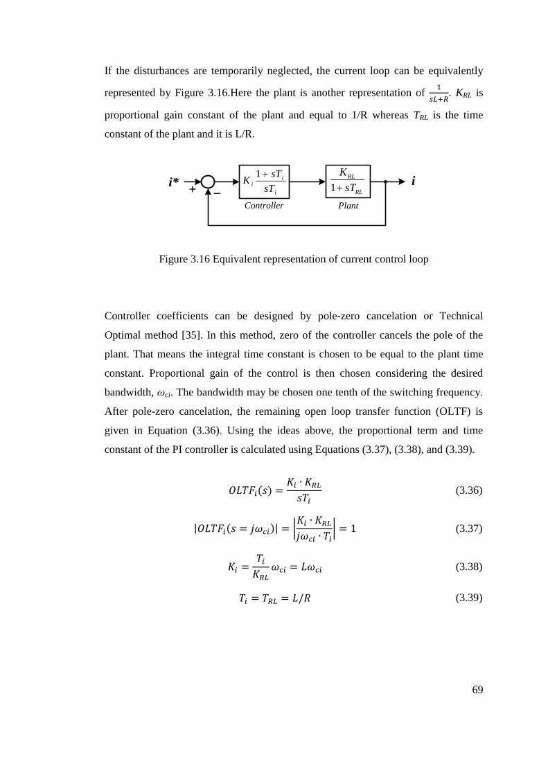
69
If the disturbances are temporarily neglected, the current loop can be equivalently
represented by Figure 3.16.Here the plant is another representation of
. KRL is
proportional gain constant of the plant and equal to 1/R whereas TRL is the time
constant of the plant and it is L/R.
+ _i* 1
RL
RL
K
sTi
Controller Plant
i
ii
sT
sTK
1
Figure 3.16 Equivalent representation of current control loop
Controller coefficients can be designed by pole-zero cancelation or Technical
Optimal method [35]. In this method, zero of the controller cancels the pole of the
plant. That means the integral time constant is chosen to be equal to the plant time
constant. Proportional gain of the control is then chosen considering the desired
bandwidth, ωci. The bandwidth may be chosen one tenth of the switching frequency.
After pole-zero cancelation, the remaining open loop transfer function (OLTF) is
given in Equation (3.36). Using the ideas above, the proportional term and time
constant of the PI controller is calculated using Equations (3.37), (3.38), and (3.39).
(3.36)
(3.37)
(3.38)
(3.39)
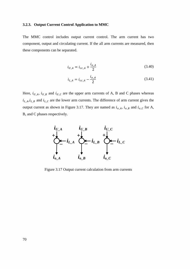
70
3.2.3. Output Current Control Application to MMC
The MMC control includes output current control. The arm current has two
component, output and circulating current. If the all arm currents are measured, then
these components can be separated.
(3.40)
(3.41)
Here, , and are the upper arm currents of A, B and C phases whereas
, and are the lower arm currents. The difference of arm current gives the
output current as shown in Figure 3.17. They are named as , and for A,
B, and C phases respectively.
_+
iU_A
iL_A
io_A
+
iU_B
iL_B
io_B
+
iU_C
iL_C
io_C
_ _
Figure 3.17 Output current calculation from arm currents

71
½Larm½Rarm LgridRgrid Ea
io_A
½vLU_A
O N½Larm½Rarm LgridRgrid Eb
io_B
½vLU_B
½Larm½Rarm LgridRgrid Ec
io_C
½vLU_C
Output
Terminal
Figure 3.18 Equivalent model of MMC for output current
The equivalent model for output current is represented in Figure 3.18 by the help of
Equations (2.16). It is similar to Figure 3.7 where the system dynamics includes first
order RL load. Notice that MMC has the half of arm impedance as output impedance
in series to generated voltage. Therefore, the impedances in Figure 3.7 and ongoing
analysis may be replaced with
and
in order
to apply the general VSC analysis to MMC case.Then, the PI controller parameters
can be tuned using Equations (3.36), (3.37), (3.38), and (3.39).
In the application, overall structure of the current controller in dq-frame is given in
Figure 3.19.
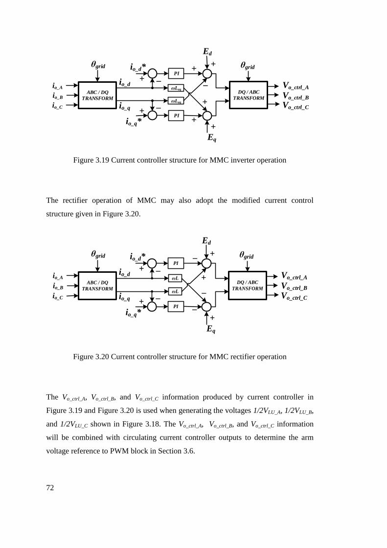
72
io_q*+
+ _
_
PI
PI
DQ / ABC
TRANSFORM
io_q
Vo_ctrl_A
θgrid io_d*
Vo_ctrl_B
Vo_ctrl_C
io_A
io_B
io_C
θgrid
Eq
Ed
ωLeq
ωLeq
ABC / DQ
TRANSFORM
+
io_d
+
++
_
+
Figure 3.19 Current controller structure for MMC inverter operation
The rectifier operation of MMC may also adopt the modified current control
structure given in Figure 3.20.
io_q*+
+ _
_
PI
PI
DQ / ABC
TRANSFORM
io_q
Vo_ctrl_A
θgrid io_d*
Vo_ctrl_B
Vo_ctrl_C
io_A
io_B
io_C
θgrid
Eq
Ed
ωL
ωL
ABC / DQ
TRANSFORM
+
io_d
_
+
+_
_
Figure 3.20 Current controller structure for MMC rectifier operation
The Vo_ctrl_A, Vo_ctrl_B, and Vo_ctrl_C information produced by current controller in
Figure 3.19 and Figure 3.20 is used when generating the voltages 1/2VLU_A, 1/2VLU_B,
and 1/2VLU_C shown in Figure 3.18. The Vo_ctrl_A, Vo_ctrl_B, and Vo_ctrl_C information
will be combined with circulating current controller outputs to determine the arm
voltage reference to PWM block in Section 3.6.

73
3.3. DC-link Voltage Control
3.3.1. Voltage Control Basics
DC-link voltage control is related to controlling the charge accumulation in the DC-
link capacitor. Basic electrical equation of the capacitor is
where and
are capacitor voltage and current, respectively.
VCiC sC1
Figure 3.21 Capacitor electrical model
If the voltage on the capacitor is desired to follow a reference value, the current of
the capacitor should be adjusted as seen in Figure 3.21. Therefore, a feedback
controller that automatically determine the required current may be used. Following
the basic electrical equation of capacitor, voltage controller ideally outputs the
required capacitor current to control its voltage as shown in Figure 3.22.
+
_Cv(s)VC
*VC
iC
sC1
Figure 3.22 Basic capacitor voltage control
The same as the current loop, voltage loop also needs an actuator to produce the
current that the voltage controller orders, shown in Figure 3.23. In real application,
the actuator of the voltage loop is the inductor or, with more general terms, current
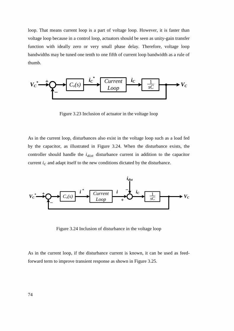
74
loop. That means current loop is a part of voltage loop. However, it is faster than
voltage loop because in a control loop, actuators should be seen as unity-gain transfer
function with ideally zero or very small phase delay. Therefore, voltage loop
bandwidths may be tuned one tenth to one fifth of current loop bandwidth as a rule of
thumb.
+
_Cv(s)VC
*VC
iCiC*
sC1Current
Loop
Figure 3.23 Inclusion of actuator in the voltage loop
As in the current loop, disturbances also exist in the voltage loop such as a load fed
by the capacitor, as illustrated in Figure 3.24. When the disturbance exists, the
controller should handle the disturbance current in addition to the capacitor
current and adapt itself to the new conditions dictated by the disturbance.
+
_Cv(s)VC
*VC
iCi *
i
idist
+
_
sC1Current
Loop
Figure 3.24 Inclusion of disturbance in the voltage loop
As in the current loop, if the disturbance current is known, it can be used as feed-
forward term to improve transient response as shown in Figure 3.25.
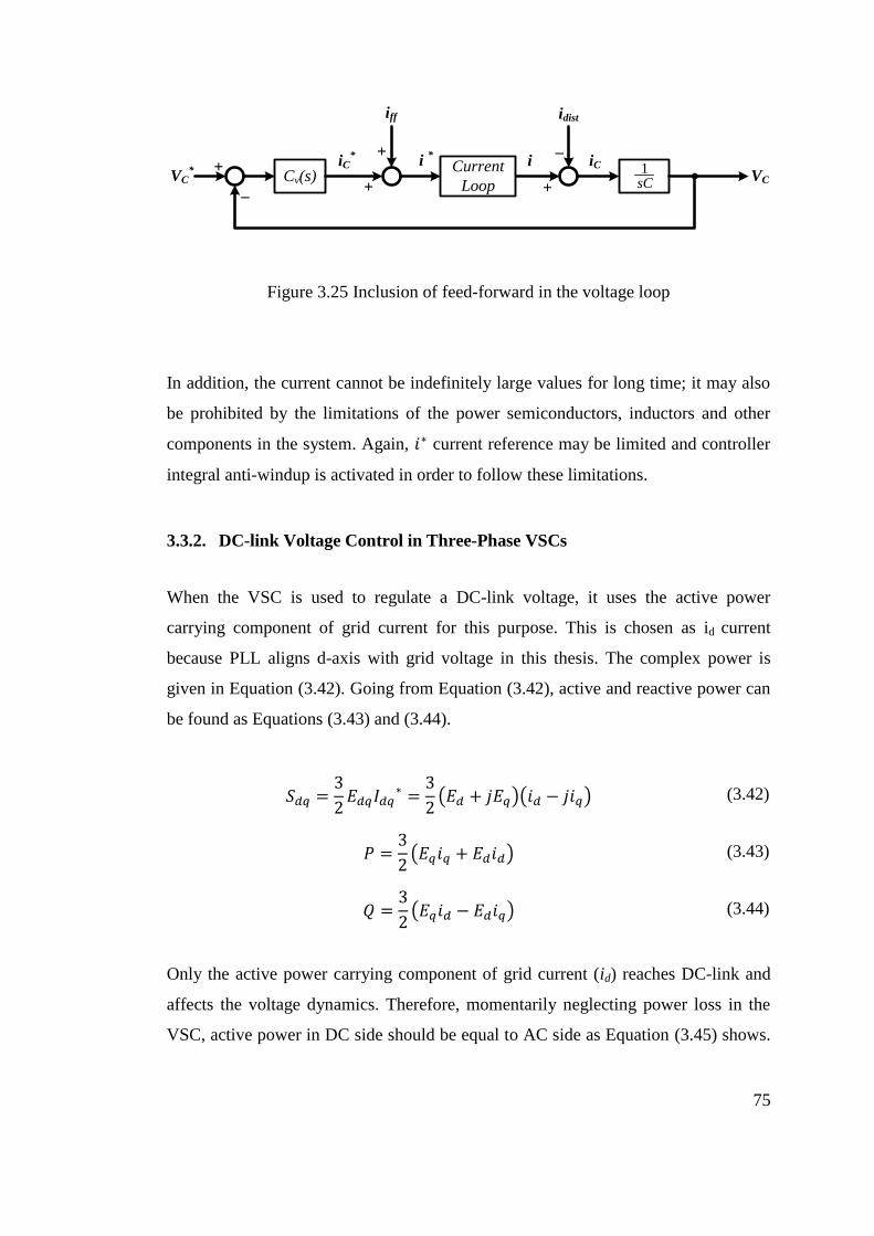
75
+
_Cv(s)VC
*VC
iCiC*
i
idist
+
_
+
+i
*
iff
sC1Current
Loop
Figure 3.25 Inclusion of feed-forward in the voltage loop
In addition, the current cannot be indefinitely large values for long time; it may also
be prohibited by the limitations of the power semiconductors, inductors and other
components in the system. Again, current reference may be limited and controller
integral anti-windup is activated in order to follow these limitations.
3.3.2. DC-link Voltage Control in Three-Phase VSCs
When the VSC is used to regulate a DC-link voltage, it uses the active power
carrying component of grid current for this purpose. This is chosen as id current
because PLL aligns d-axis with grid voltage in this thesis. The complex power is
given in Equation (3.42). Going from Equation (3.42), active and reactive power can
be found as Equations (3.43) and (3.44).
(3.42)
(3.43)
(3.44)
Only the active power carrying component of grid current (id) reaches DC-link and
affects the voltage dynamics. Therefore, momentarily neglecting power loss in the
VSC, active power in DC side should be equal to AC side as Equation (3.45) shows.
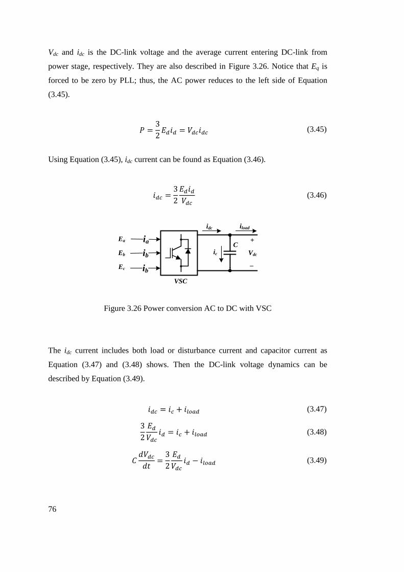
76
Vdc and idc is the DC-link voltage and the average current entering DC-link from
power stage, respectively. They are also described in Figure 3.26. Notice that Eq is
forced to be zero by PLL; thus, the AC power reduces to the left side of Equation
(3.45).
(3.45)
Using Equation (3.45), idc current can be found as Equation (3.46).
(3.46)
idc iload
ic
C
Vdc
+
_
Ea
Eb
Ec
VSC
ia
ib
ib
Figure 3.26 Power conversion AC to DC with VSC
The idc current includes both load or disturbance current and capacitor current as
Equation (3.47) and (3.48) shows. Then the DC-link voltage dynamics can be
described by Equation (3.49).
(3.47)
(3.48)
(3.49)
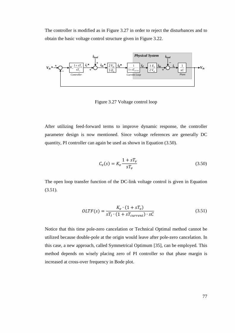
77
The controller is modified as in Figure 3.27 in order to reject the disturbances and to
obtain the basic voltage control structure given in Figure 3.22.
+_
Vdc*1
sCVdc
Controller Plant
dc
d
V
E
2
3
Current Loop
currentsT1
1 idid* idc ic
iload
+
_
îload
ic*
+
+
d
dc
E
V
3
2idc*
Physical System
v
vv
sT
sTK
1
Figure 3.27 Voltage control loop
After utilizing feed-forward terms to improve dynamic response, the controller
parameter design is now mentioned. Since voltage references are generally DC
quantity, PI controller can again be used as shown in Equation (3.50).
(3.50)
The open loop transfer function of the DC-link voltage control is given in Equation
(3.51).
(3.51)
Notice that this time pole-zero cancelation or Technical Optimal method cannot be
utilized because double-pole at the origin would leave after pole-zero cancelation. In
this case, a new approach, called Symmetrical Optimum [35], can be employed. This
method depends on wisely placing zero of PI controller so that phase margin is
increased at cross-over frequency in Bode plot.
78
In the voltage loop, close loop current loop in Equation (3.51) is represented by
1/(1+sTcurrent) which is derived in Equations (3.52), (3.53), and (3.54).
(3.52)
(3.53)
(3.54)
In Symmetrical Optimum method, the factor “a” is defined. It is a coefficient to
simplify the analysis. The damping factor is represented by ζ and phase margin by ψ
in Equation (3.55). For the voltage loop, the cross-over frequency is now ωcv which is
formulized in Equation (3.56). The proportional gain and time constant of PI
controller is given in Equations (3.57) and (3.58).
(3.55)
(3.56)
(3.57)
(3.58)
Generally, the factor “a” is expected to be greater than 2.4 because the damping
factor ζ is 0.7 at least. After choosing the factor "a" or the cross-over frequency for
the voltage loop, the PI parameters can be found using Equations (3.57) and (3.58).
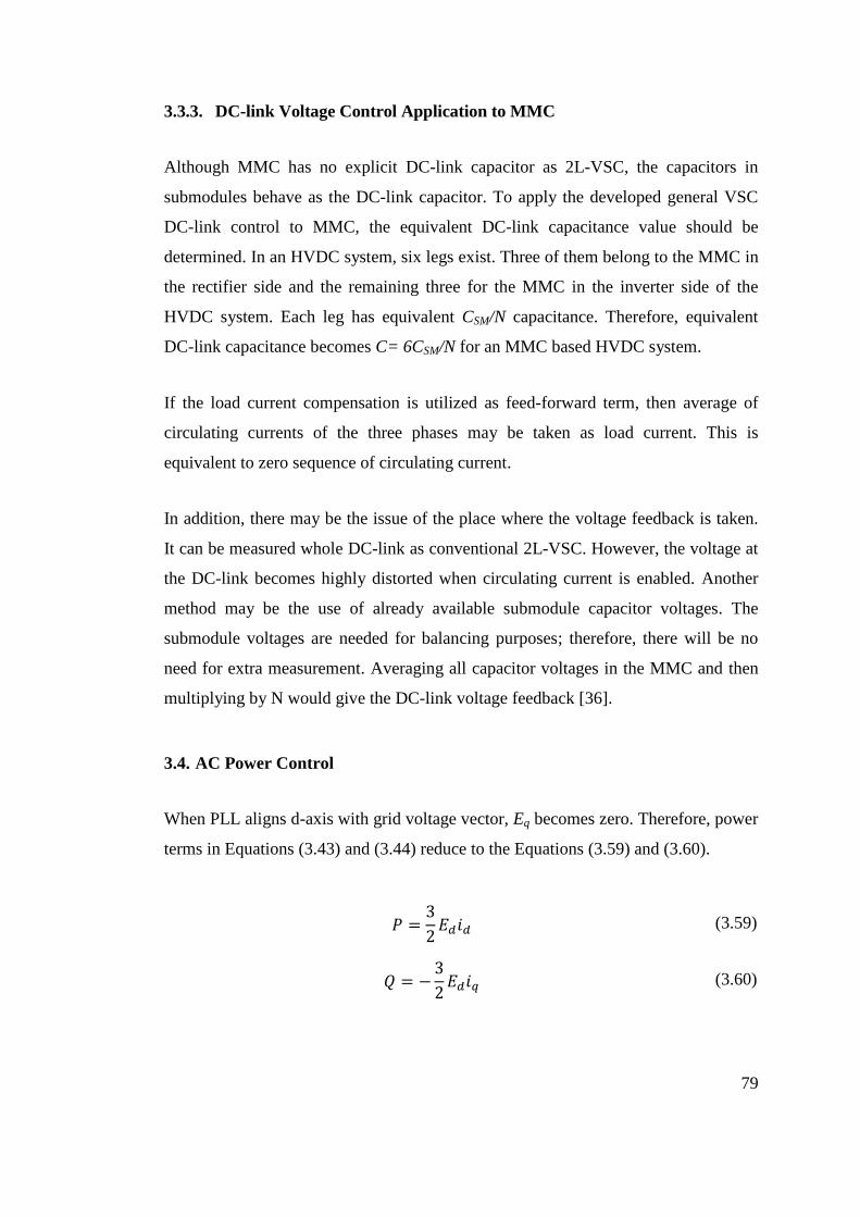
79
3.3.3. DC-link Voltage Control Application to MMC
Although MMC has no explicit DC-link capacitor as 2L-VSC, the capacitors in
submodules behave as the DC-link capacitor. To apply the developed general VSC
DC-link control to MMC, the equivalent DC-link capacitance value should be
determined. In an HVDC system, six legs exist. Three of them belong to the MMC in
the rectifier side and the remaining three for the MMC in the inverter side of the
HVDC system. Each leg has equivalent CSM/N capacitance. Therefore, equivalent
DC-link capacitance becomes C= 6CSM/N for an MMC based HVDC system.
If the load current compensation is utilized as feed-forward term, then average of
circulating currents of the three phases may be taken as load current. This is
equivalent to zero sequence of circulating current.
In addition, there may be the issue of the place where the voltage feedback is taken.
It can be measured whole DC-link as conventional 2L-VSC. However, the voltage at
the DC-link becomes highly distorted when circulating current is enabled. Another
method may be the use of already available submodule capacitor voltages. The
submodule voltages are needed for balancing purposes; therefore, there will be no
need for extra measurement. Averaging all capacitor voltages in the MMC and then
multiplying by N would give the DC-link voltage feedback [36].
3.4. AC Power Control
When PLL aligns d-axis with grid voltage vector, Eq becomes zero. Therefore, power
terms in Equations (3.43) and (3.44) reduce to the Equations (3.59) and (3.60).
(3.59)
(3.60)

80
Considering the power equations in Equations (3.59) and (3.60), the only variable to
control power is either id for active power or iq for reactive power. Since Ed value is
constant and known to the controller due to PLL, active and reactive power can be
controlled linearly with changing id or iq, respectively.
The power controller can be open loop where only id or iq current references to
current controllers are calculated using Equations (3.59) and (3.60) and desired
power references as described in Figure 3.28 and Figure 3.29.
P*id*
Current Loop
currentsT1
1 id
dE2
3P
dE
1
3
2
Figure 3.28 Active power open loop control
Q*iq*
Current Loop
currentsT1
1 iq
dE2
3 Q
dE
1
3
2
Figure 3.29 Reactive power open loop control
In addition to this, close loop control is also possible as shown in Figure 3.30 and
Figure 3.31. In this case, a PI controller decides id* or iq* reference. Then, measured
id and iq currents and Ed voltage may be used to find power feedback value.
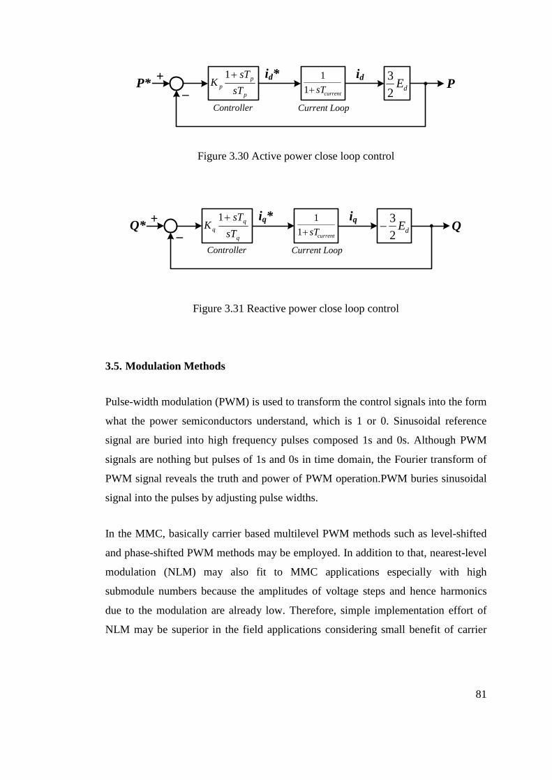
81
+_
P*
Controller
id*
p
p
psT
sTK
1
Current Loop
currentsT1
1 id
dE2
3P
Figure 3.30 Active power close loop control
+_
Q*
Controller
iq*
q
q
qsT
sTK
1
Current Loop
currentsT1
1 iq
dE2
3 Q
Figure 3.31 Reactive power close loop control
3.5. Modulation Methods
Pulse-width modulation (PWM) is used to transform the control signals into the form
what the power semiconductors understand, which is 1 or 0. Sinusoidal reference
signal are buried into high frequency pulses composed 1s and 0s. Although PWM
signals are nothing but pulses of 1s and 0s in time domain, the Fourier transform of
PWM signal reveals the truth and power of PWM operation.PWM buries sinusoidal
signal into the pulses by adjusting pulse widths.
In the MMC, basically carrier based multilevel PWM methods such as level-shifted
and phase-shifted PWM methods may be employed. In addition to that, nearest-level
modulation (NLM) may also fit to MMC applications especially with high
submodule numbers because the amplitudes of voltage steps and hence harmonics
due to the modulation are already low. Therefore, simple implementation effort of
NLM may be superior in the field applications considering small benefit of carrier
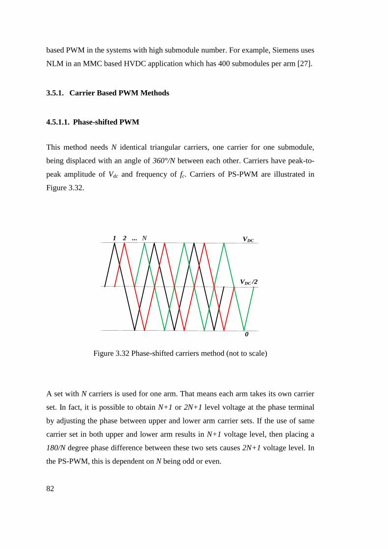
82
based PWM in the systems with high submodule number. For example, Siemens uses
NLM in an MMC based HVDC application which has 400 submodules per arm [27].
3.5.1. Carrier Based PWM Methods
4.5.1.1. Phase-shifted PWM
This method needs N identical triangular carriers, one carrier for one submodule,
being displaced with an angle of 360°/N between each other. Carriers have peak-to-
peak amplitude of Vdc and frequency of fc. Carriers of PS-PWM are illustrated in
Figure 3.32.
VDC
0
1 ... N2
VDC /2
Figure 3.32 Phase-shifted carriers method (not to scale)
A set with N carriers is used for one arm. That means each arm takes its own carrier
set. In fact, it is possible to obtain N+1 or 2N+1 level voltage at the phase terminal
by adjusting the phase between upper and lower arm carrier sets. If the use of same
carrier set in both upper and lower arm results in N+1 voltage level, then placing a
180/N degree phase difference between these two sets causes 2N+1 voltage level. In
the PS-PWM, this is dependent on N being odd or even.
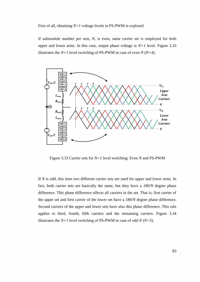
83
First of all, obtaining N+1 voltage levels in PS-PWM is explored.
If submodule number per arm, N, is even, same carrier set is employed for both
upper and lower arms. In this case, output phase voltage is N+1 level. Figure 3.33
illustrates the N+1 level switching of PS-PWM in case of even N (N=4).
SM-3
SM-4
SM-1
SM-2
SM-3
O
VDC/2
VDC/2
SM-4
Larm
Rarm
Rarm
Larm
SM-1
SM-2
1 2 3 4Vdc
0
Upper
Arm
Carriers
1 2 3 4Vdc
0
Lower
Arm
Carriers
Figure 3.33 Carrier sets for N+1 level switching: Even N and PS-PWM
If N is odd, this time two different carrier sets are used for upper and lower arms. In
fact, both carrier sets are basically the same, but they have a 180/N degree phase
difference. This phase difference affects all carriers in the set. That is, first carrier of
the upper set and first carrier of the lower set have a 180/N degree phase difference.
Second carriers of the upper and lower sets have also this phase difference. This rule
applies to third, fourth, fifth carriers and the remaining carriers. Figure 3.34
illustrates the N+1 level switching of PS-PWM in case of odd N (N=5).
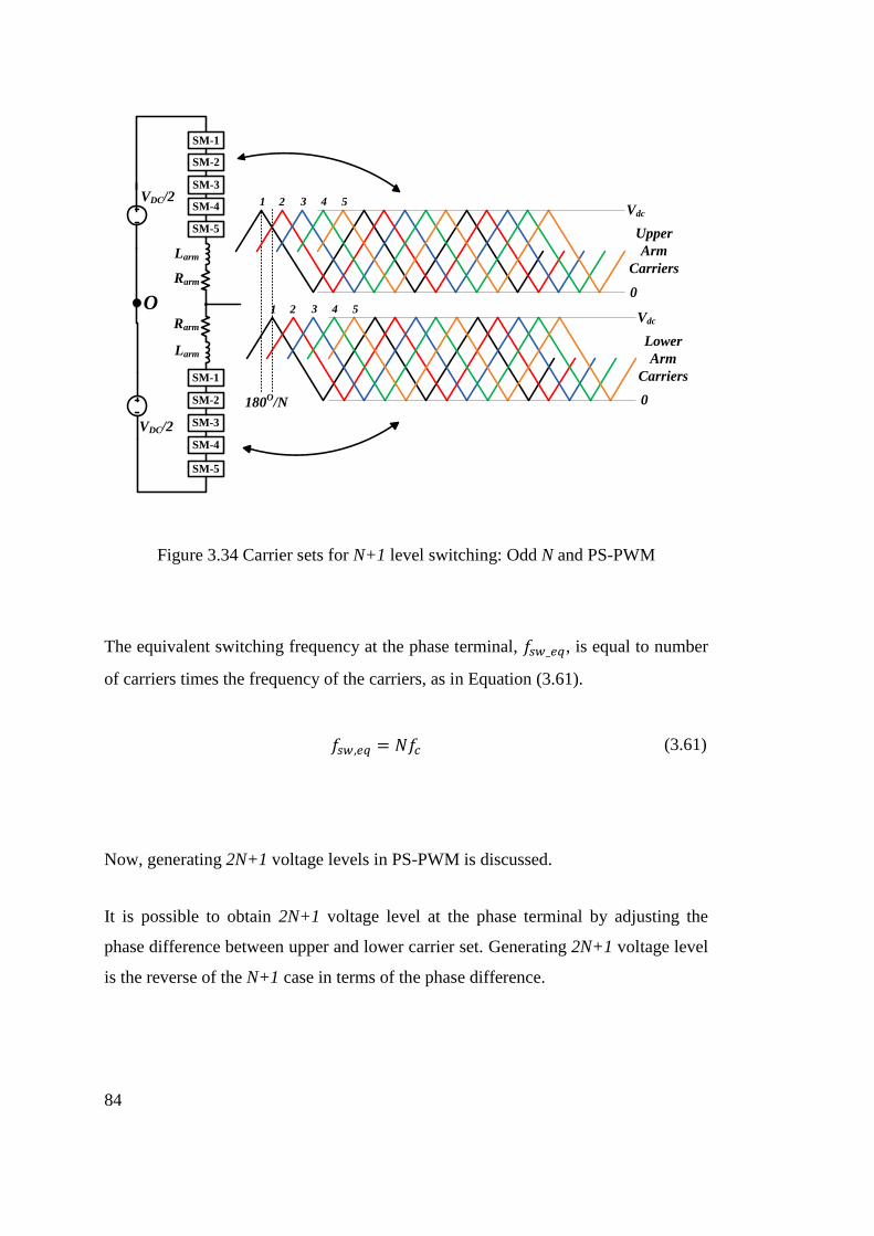
84
1 2 3 4 5Vdc
01 2 3 4 5
Vdc
0180O/N
Upper
Arm
Carriers
Lower
Arm
Carriers
SM-3
SM-4
SM-5
SM-1
SM-2
SM-3
O
VDC/2
VDC/2
SM-4
SM-5
Larm
Rarm
Rarm
Larm
SM-1
SM-2
Figure 3.34 Carrier sets for N+1 level switching: Odd N and PS-PWM
The equivalent switching frequency at the phase terminal, , is equal to number
of carriers times the frequency of the carriers, as in Equation (3.61).
(3.61)
Now, generating 2N+1 voltage levels in PS-PWM is discussed.
It is possible to obtain 2N+1 voltage level at the phase terminal by adjusting the
phase difference between upper and lower carrier set. Generating 2N+1 voltage level
is the reverse of the N+1 case in terms of the phase difference.
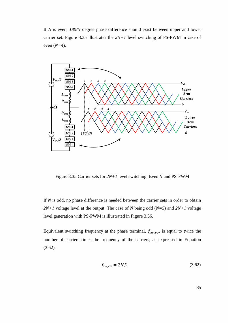
85
If N is even, 180/N degree phase difference should exist between upper and lower
carrier set. Figure 3.35 illustrates the 2N+1 level switching of PS-PWM in case of
even (N=4).
SM-3
SM-4
SM-1
SM-2
SM-3
O
VDC/2
VDC/2
SM-4
Larm
Rarm
Rarm
Larm
SM-1
SM-2
1 2 3 4Vdc
0
Upper
Arm
Carriers
1 2 3 4Vdc
0
Lower
Arm
Carriers
180O/N
Figure 3.35 Carrier sets for 2N+1 level switching: Even N and PS-PWM
If N is odd, no phase difference is needed between the carrier sets in order to obtain
2N+1 voltage level at the output. The case of N being odd (N=5) and 2N+1 voltage
level generation with PS-PWM is illustrated in Figure 3.36.
Equivalent switching frequency at the phase terminal, , is equal to twice the
number of carriers times the frequency of the carriers, as expressed in Equation
(3.62).
(3.62)
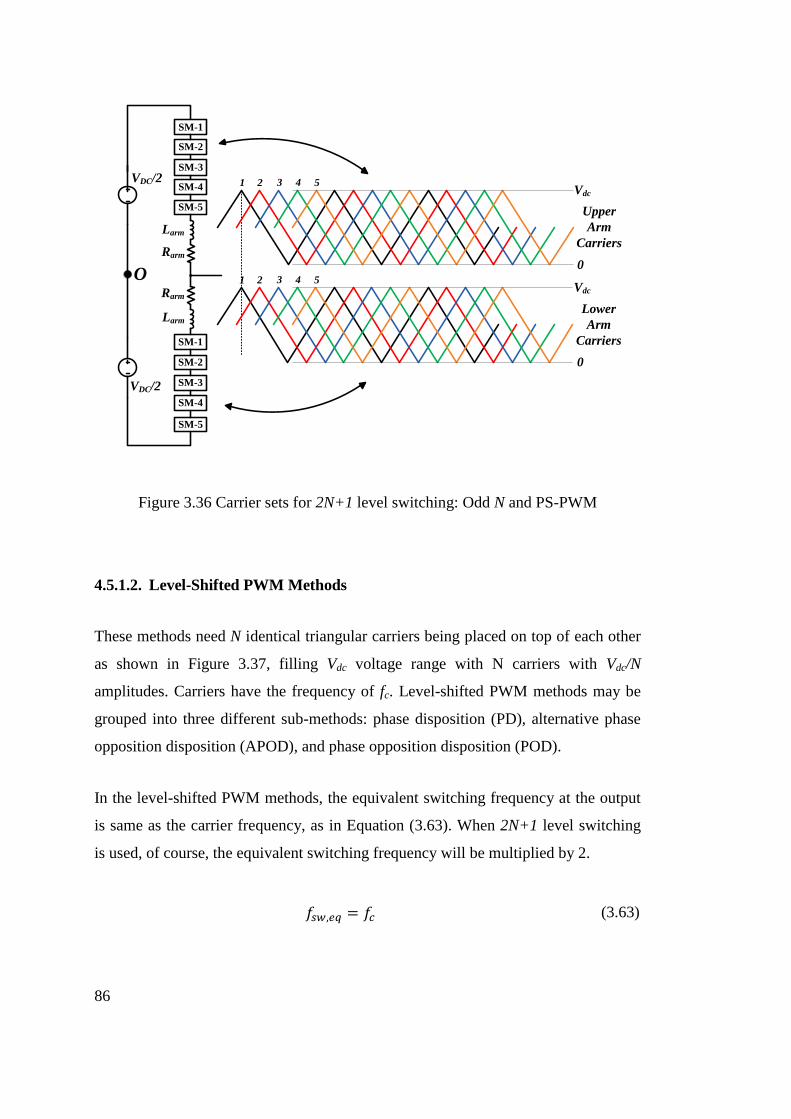
86
1 2 3 4 5Vdc
01 2 3 4 5
Vdc
0
Upper
Arm
Carriers
Lower
Arm
Carriers
SM-3
SM-4
SM-5
SM-1
SM-2
SM-3
O
VDC/2
VDC/2
SM-4
SM-5
Larm
Rarm
Rarm
Larm
SM-1
SM-2
Figure 3.36 Carrier sets for 2N+1 level switching: Odd N and PS-PWM
4.5.1.2. Level-Shifted PWM Methods
These methods need N identical triangular carriers being placed on top of each other
as shown in Figure 3.37, filling Vdc voltage range with N carriers with Vdc/N
amplitudes. Carriers have the frequency of fc. Level-shifted PWM methods may be
grouped into three different sub-methods: phase disposition (PD), alternative phase
opposition disposition (APOD), and phase opposition disposition (POD).
In the level-shifted PWM methods, the equivalent switching frequency at the output
is same as the carrier frequency, as in Equation (3.63). When 2N+1 level switching
is used, of course, the equivalent switching frequency will be multiplied by 2.
(3.63)
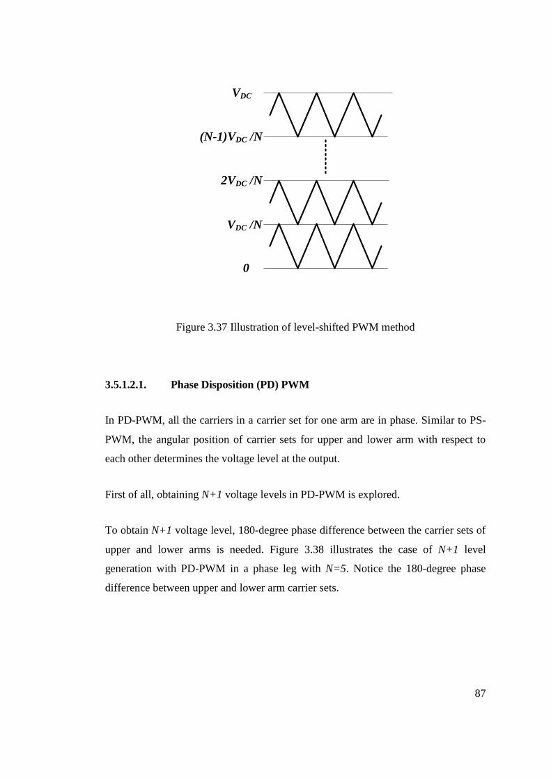
87
VDC /N
2VDC /N
0
VDC
(N-1)VDC /N
Figure 3.37 Illustration of level-shifted PWM method
3.5.1.2.1. Phase Disposition (PD) PWM
In PD-PWM, all the carriers in a carrier set for one arm are in phase. Similar to PS-
PWM, the angular position of carrier sets for upper and lower arm with respect to
each other determines the voltage level at the output.
First of all, obtaining N+1 voltage levels in PD-PWM is explored.
To obtain N+1 voltage level, 180-degree phase difference between the carrier sets of
upper and lower arms is needed. Figure 3.38 illustrates the case of N+1 level
generation with PD-PWM in a phase leg with N=5. Notice the 180-degree phase
difference between upper and lower arm carrier sets.
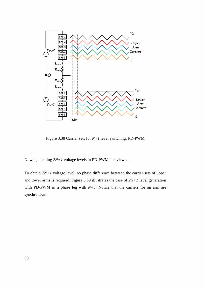
88
SM-3
SM-4
SM-5
SM-1
SM-2
SM-3
O
VDC/2
VDC/2
SM-4
SM-5
Larm
Rarm
Rarm
Larm
SM-1
SM-2Upper
Arm
Carriers
Vdc
0
180O
Lower
Arm
Carriers
Vdc
0
Figure 3.38 Carrier sets for N+1 level switching: PD-PWM
Now, generating 2N+1 voltage levels in PD-PWM is reviewed.
To obtain 2N+1 voltage level, no phase difference between the carrier sets of upper
and lower arms is required. Figure 3.39 illustrates the case of 2N+1 level generation
with PD-PWM in a phase leg with N=5. Notice that the carriers for an arm are
synchronous.

89
SM-3
SM-4
SM-5
SM-1
SM-2
SM-3
O
VDC/2
VDC/2
SM-4
SM-5
Larm
Rarm
Rarm
Larm
SM-1
SM-2Upper
Arm
Carriers
Vdc
0
Lower
Arm
Carriers
Vdc
0
Figure 3.39 Carrier sets for 2N+1 level switching: PD-PWM
3.5.1.2.2. Alternative Phase Opposition Disposition (APOD) PWM
In APOD-PWM, all the carriers in a carrier set for one arm have 180-degree phase
difference with their adjacent carrier. That is, if the first carrier is taken reference and
said to have zero phase, second carrier has 180-degree phase and third carrier has
zero phase again and so on. Again, the angular position of carrier sets for upper and
lower arm with respect to each other determines the voltage level at the output.
N+1 level voltage generation with APOD-PWM is discussed first.
To obtain N+1 voltage level in APOD-PWM, 180-degree phase difference between
the carrier sets of upper and lower arms is needed. Figure 3.40 illustrates the case of
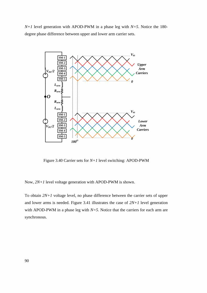
90
N+1 level generation with APOD-PWM in a phase leg with N=5. Notice the 180-
degree phase difference between upper and lower arm carrier sets.
SM-3
SM-4
SM-5
SM-1
SM-2
SM-3
O
VDC/2
VDC/2
SM-4
SM-5
Larm
Rarm
Rarm
Larm
SM-1
SM-2Upper
Arm
Carriers
Vdc
0
180O
Lower
Arm
Carriers
Vdc
0
Figure 3.40 Carrier sets for N+1 level switching: APOD-PWM
Now, 2N+1 level voltage generation with APOD-PWM is shown.
To obtain 2N+1 voltage level, no phase difference between the carrier sets of upper
and lower arms is needed. Figure 3.41 illustrates the case of 2N+1 level generation
with APOD-PWM in a phase leg with N=5. Notice that the carriers for each arm are
synchronous.

91
SM-3
SM-4
SM-5
SM-1
SM-2
SM-3
O
VDC/2
VDC/2
SM-4
SM-5
Larm
Rarm
Rarm
Larm
SM-1
SM-2 Upper
Arm
Carriers
Vdc
0
Lower
Arm
Carriers
Vdc
0
Figure 3.41 Carrier sets for 2N+1 level switching: APOD-PWM
3.5.2. Nearest-level Modulation
In the nearest-level modulation (NLM), deciding the inserted submodule number,
Non, based on the amplitude of the reference modulating signal. It makes a magnitude
comparison between the reference signal and the discrete voltages that the converter
can generate. Therefore, there is no need for carriers and PWM. This modulation
strategy is appropriate for MMC system with a high numbers of submodules because
the small voltage steps do not deteriorate output voltage quality. In addition to that,
NLM is simpler to implement for large MMC systems.

92
3.6. MMC Inner Control
MMC has only one voltage supply which is DC-link; that is, it discards complex
supply network to each individual submodule. However, this advantage does not
come for free. The price to pay for this is more complex control. Indispensible part of
this control is the voltage balancing of the submodules so that they do not diverge
and result in collapse of the system. In addition this, the researchers proposed some
methods to eliminate harmonic components of circulating current [25], [37], [38] in
order to improve efficiency.
There are two basic approaches in the inner control of MMC. First one is widely
adopted sorting algorithm based inner control method. It is proposed by Lesnicar and
Marquardt [6] who are also the first researchers to propose MMC. This method uses
sorting algorithm to balance submodule voltages. The other one is PS-PWM based
inner control approach. It is proposed by Hagiwara and Akagi [30]. It combines the
active voltage balancing controllers and phase-shifted PWM in order to achieve
balanced submodule voltages.
3.6.1. Sorting Algorithm Based Inner Control
An overall inner control structure based on sorting algorithm is shown in Figure 3.42.
Notice that this is for one phase only. A three-phase system requires three of them to
control all the phases. The control signals from output current control, Vo_ctrl_x, and
circulating current control, Vcc_ctrl_x, are combined at first. Notice that lower arm
takes Vo_ctrl_x positive while upper arm negative.
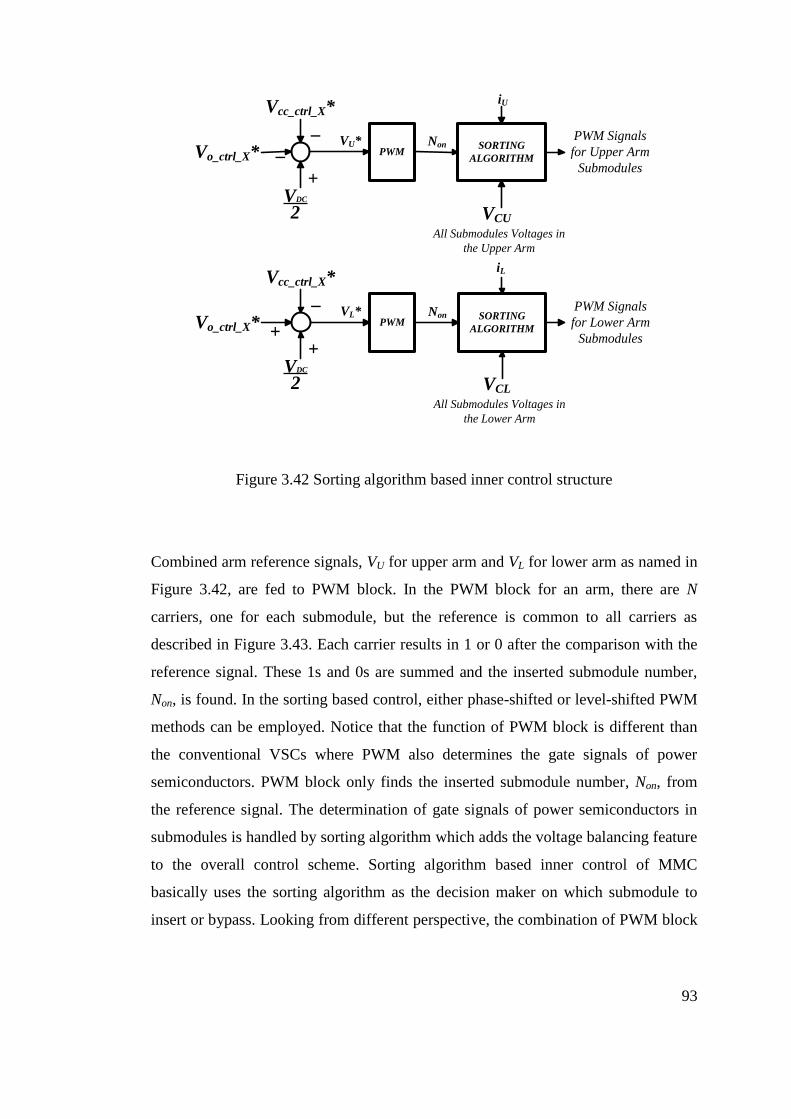
93
_
VDC
2
Vo_ctrl_X*
Vcc_ctrl_X*
+
_
PWM
PWM Signals
for Upper Arm
Submodules
VCU
All Submodules Voltages in
the Upper Arm
SORTING
ALGORITHM
NonVU*
VDC
2
Vo_ctrl_X*
Vcc_ctrl_X*
+
_
PWM
PWM Signals
for Lower Arm
Submodules
VCL
All Submodules Voltages in
the Lower Arm
SORTING
ALGORITHM
NonVL*
+
iU
iL
Figure 3.42 Sorting algorithm based inner control structure
Combined arm reference signals, VU for upper arm and VL for lower arm as named in
Figure 3.42, are fed to PWM block. In the PWM block for an arm, there are N
carriers, one for each submodule, but the reference is common to all carriers as
described in Figure 3.43. Each carrier results in 1 or 0 after the comparison with the
reference signal. These 1s and 0s are summed and the inserted submodule number,
Non, is found. In the sorting based control, either phase-shifted or level-shifted PWM
methods can be employed. Notice that the function of PWM block is different than
the conventional VSCs where PWM also determines the gate signals of power
semiconductors. PWM block only finds the inserted submodule number, Non, from
the reference signal. The determination of gate signals of power semiconductors in
submodules is handled by sorting algorithm which adds the voltage balancing feature
to the overall control scheme. Sorting algorithm based inner control of MMC
basically uses the sorting algorithm as the decision maker on which submodule to
insert or bypass. Looking from different perspective, the combination of PWM block
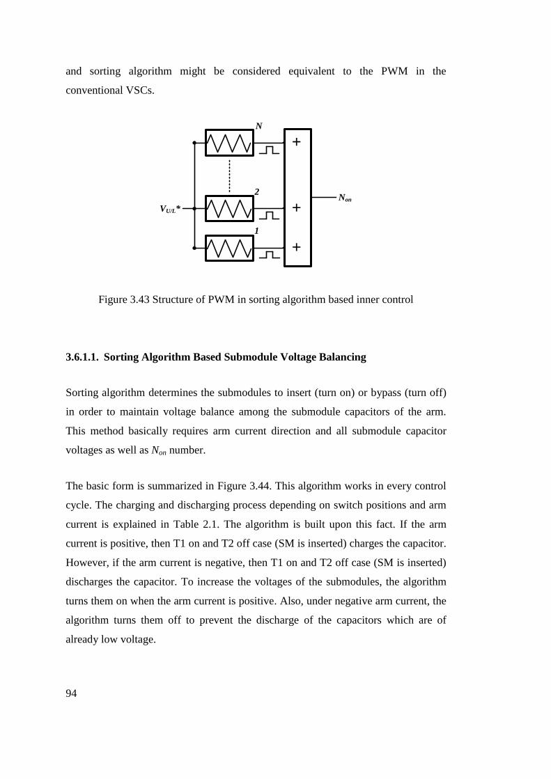
94
and sorting algorithm might be considered equivalent to the PWM in the
conventional VSCs.
+
+
+
1
N
2Non
VU/L*
Figure 3.43 Structure of PWM in sorting algorithm based inner control
3.6.1.1. Sorting Algorithm Based Submodule Voltage Balancing
Sorting algorithm determines the submodules to insert (turn on) or bypass (turn off)
in order to maintain voltage balance among the submodule capacitors of the arm.
This method basically requires arm current direction and all submodule capacitor
voltages as well as Non number.
The basic form is summarized in Figure 3.44. This algorithm works in every control
cycle. The charging and discharging process depending on switch positions and arm
current is explained in Table 2.1. The algorithm is built upon this fact. If the arm
current is positive, then T1 on and T2 off case (SM is inserted) charges the capacitor.
However, if the arm current is negative, then T1 on and T2 off case (SM is inserted)
discharges the capacitor. To increase the voltages of the submodules, the algorithm
turns them on when the arm current is positive. Also, under negative arm current, the
algorithm turns them off to prevent the discharge of the capacitors which are of
already low voltage.
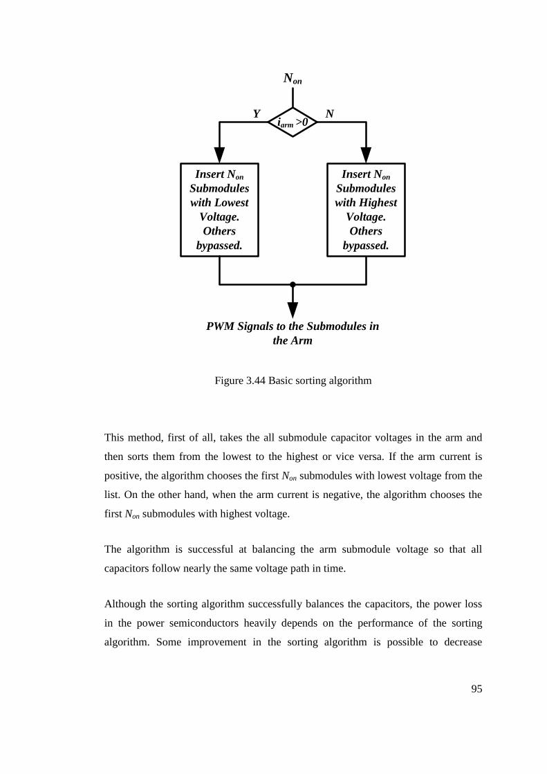
95
iarm >0
Insert Non
Submodules
with Lowest
Voltage.
Others
bypassed.
Y N
Non
PWM Signals to the Submodules in
the Arm
Insert Non
Submodules
with Highest
Voltage.
Others
bypassed.
Figure 3.44 Basic sorting algorithm
This method, first of all, takes the all submodule capacitor voltages in the arm and
then sorts them from the lowest to the highest or vice versa. If the arm current is
positive, the algorithm chooses the first Non submodules with lowest voltage from the
list. On the other hand, when the arm current is negative, the algorithm chooses the
first Non submodules with highest voltage.
The algorithm is successful at balancing the arm submodule voltage so that all
capacitors follow nearly the same voltage path in time.
Although the sorting algorithm successfully balances the capacitors, the power loss
in the power semiconductors heavily depends on the performance of the sorting
algorithm. Some improvement in the sorting algorithm is possible to decrease
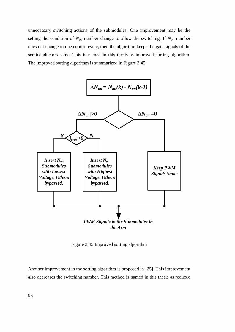
96
unnecessary switching actions of the submodules. One improvement may be the
setting the condition of Non number change to allow the switching. If Non number
does not change in one control cycle, then the algorithm keeps the gate signals of the
semiconductors same. This is named in this thesis as improved sorting algorithm.
The improved sorting algorithm is summarized in Figure 3.45.
iarm >0
Insert Non
Submodules
with Lowest
Voltage. Others
bypassed.
∆Non = Non(k) - Non(k-1)
|∆Non|>0
Y N
Insert Non
Submodules
with Highest
Voltage. Others
bypassed.
Keep PWM
Signals Same
∆Non =0
PWM Signals to the Submodules in
the Arm
Figure 3.45 Improved sorting algorithm
Another improvement in the sorting algorithm is proposed in [25]. This improvement
also decreases the switching number. This method is named in this thesis as reduced
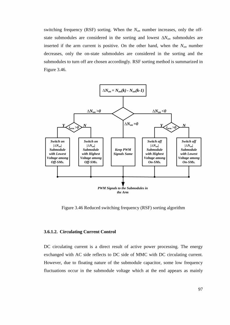
97
switching frequency (RSF) sorting. When the Non number increases, only the off-
state submodules are considered in the sorting and lowest ∆Non submodules are
inserted if the arm current is positive. On the other hand, when the Non number
decreases, only the on-state submodules are considered in the sorting and the
submodules to turn off are chosen accordingly. RSF sorting method is summarized in
Figure 3.46.
iarm >0
Switch on
|∆Non|
Submodule
with Lowest
Voltage among
Off-SMs.
∆Non <0
∆Non = Non(k) - Non(k-1)
∆Non >0
iarm >0Y Y NN
Switch on
|∆Non| Submodule
with Highest
Voltage among
Off-SMs.
Keep PWM
Signals Same
Switch off
|∆Non|
Submodule
with Highest
Voltage among
On-SMs.
∆Non =0
Switch off
|∆Non|
Submodule
with Lowest
Voltage among
On-SMs.
PWM Signals to the Submodules in
the Arm
Figure 3.46 Reduced switching frequency (RSF) sorting algorithm
3.6.1.2. Circulating Current Control
DC circulating current is a direct result of active power processing. The energy
exchanged with AC side reflects to DC side of MMC with DC circulating current.
However, due to floating nature of the submodule capacitor, some low frequency
fluctuations occur in the submodule voltage which at the end appears as mainly
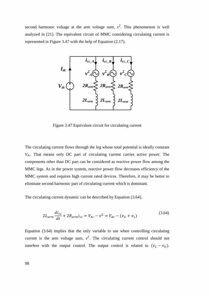
98
second harmonic voltage at the arm voltage sum, vΣ. This phenomenon is well
analyzed in [21]. The equivalent circuit of MMC considering circulating current is
represented in Figure 3.47 with the help of Equation (2.17).
Vdc
2Larm
2Rarm
icc_A
vΣ
B vΣ
CvΣ
A
icc_B icc_C
Idc
2Rarm2Rarm
2Larm 2Larm
Figure 3.47 Equivalent circuit for circulating current
The circulating current flows through the leg whose total potential is ideally constant
Vdc. That means only DC part of circulating current carries active power. The
components other than DC part can be considered as reactive power flow among the
MMC legs. As in the power system, reactive power flow decreases efficiency of the
MMC system and requires high current rated devices. Therefore, it may be better to
eliminate second harmonic part of circulating current which is dominant.
The circulating current dynamic can be described by Equation (3.64).
(3.64)
Equation (3.64) implies that the only variable to use when controlling circulating
current is the arm voltage sum, vΣ. The circulating current control should not
interfere with the output control. The output control is related to .

99
Therefore, circulating current control should appear in , but disappear in
. This leads to adding (or subtracting) circulating current control signal
with equal amount to both arm voltage reference, and , as Figure 3.42 shows.
The circulating current dynamics is written again in Equation (3.65) by splitting arm
voltage sum, vΣ, into DC-link voltage and circulating current driving terms, Vdc and
Vcc, respectively. Notice that (Vdc-2Vcc)/2 is common in the arm voltage reference of
both arm as shown in Figure 3.42. Vcc takes the coefficient of 2 because it represents
control signal is shared by both arms as discussed in the above paragraph. As a
result, the current dynamics reduces to Equation (3.66).
(3.65)
(3.66)
The time domain dynamics of the three phase-legs are given in Equations(3.67),
(3.68), and (3.69).
(3.67)
(3.68)
(3.69)
Because the controlled part of the circulating current is second harmonic; the
currents are formulized in Equations (3.70), (3.71), and (3.72). The phases of the
current are given according to the fact that second harmonic is negative sequence.
Since DC term is zero sequence, the rotating circulating current vector is described in
Equation (3.73). Notice that the rotation is in negative direction as the angle (-
2ωt+φ) shows.
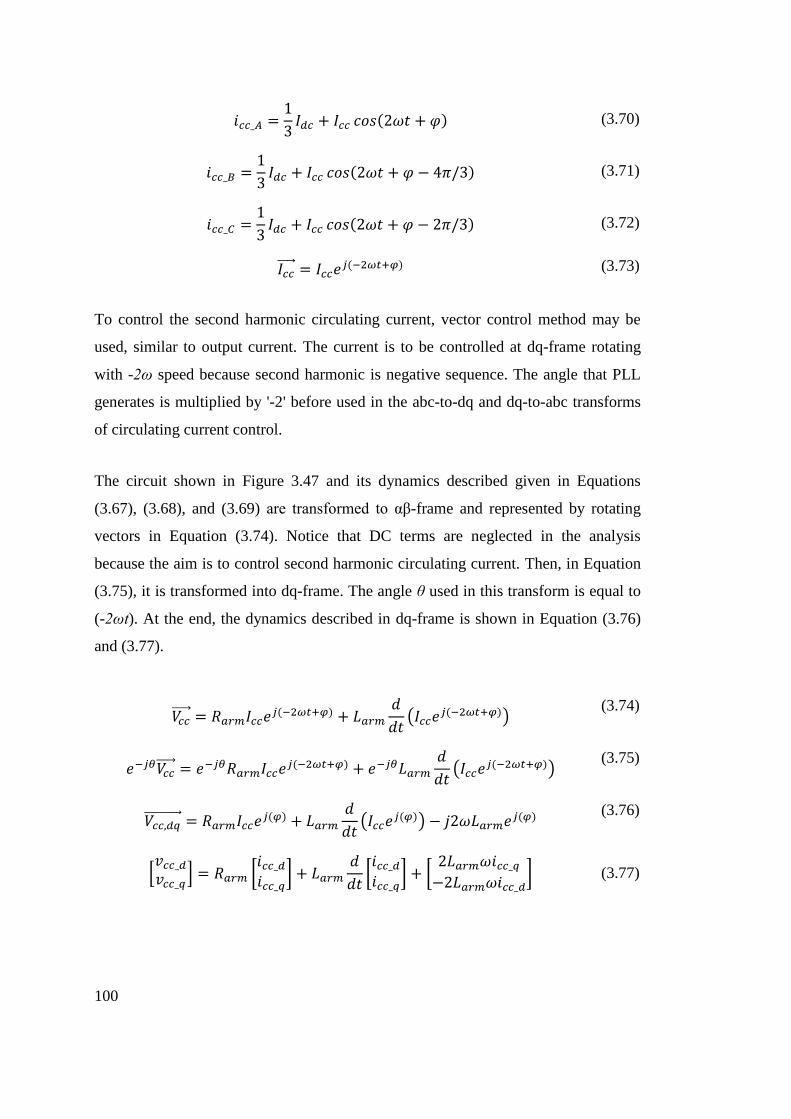
100
(3.70)
(3.71)
(3.72)
(3.73)
To control the second harmonic circulating current, vector control method may be
used, similar to output current. The current is to be controlled at dq-frame rotating
with -2ω speed because second harmonic is negative sequence. The angle that PLL
generates is multiplied by '-2' before used in the abc-to-dq and dq-to-abc transforms
of circulating current control.
The circuit shown in Figure 3.47 and its dynamics described given in Equations
(3.67), (3.68), and (3.69) are transformed to αβ-frame and represented by rotating
vectors in Equation (3.74). Notice that DC terms are neglected in the analysis
because the aim is to control second harmonic circulating current. Then, in Equation
(3.75), it is transformed into dq-frame. The angle θ used in this transform is equal to
(-2ωt). At the end, the dynamics described in dq-frame is shown in Equation (3.76)
and (3.77).
(3.74)
(3.75)
(3.76)
(3.77)
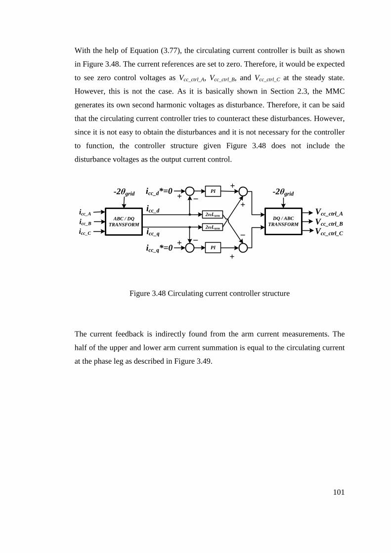
101
With the help of Equation (3.77), the circulating current controller is built as shown
in Figure 3.48. The current references are set to zero. Therefore, it would be expected
to see zero control voltages as Vcc_ctrl_A, Vcc_ctrl_B, and Vcc_ctrl_C at the steady state.
However, this is not the case. As it is basically shown in Section 2.3, the MMC
generates its own second harmonic voltages as disturbance. Therefore, it can be said
that the circulating current controller tries to counteract these disturbances. However,
since it is not easy to obtain the disturbances and it is not necessary for the controller
to function, the controller structure given Figure 3.48 does not include the
disturbance voltages as the output current control.
icc_q*=0
+ _
_
PI
PI
DQ / ABC
TRANSFORM
icc_q
Vcc_ctrl_A
-2θgrid icc_d*=0
Vcc_ctrl_B
Vcc_ctrl_C
icc_A
icc_B
icc_C
-2θgrid
2ωLarm
2ωLarm
ABC / DQ
TRANSFORM
+
icc_d
+
+
+
_
Figure 3.48 Circulating current controller structure
The current feedback is indirectly found from the arm current measurements. The
half of the upper and lower arm current summation is equal to the circulating current
at the phase leg as described in Figure 3.49.
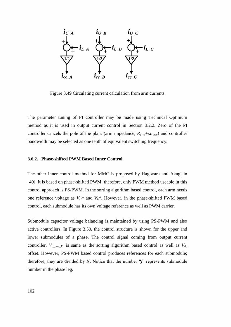
102
1/2
+
+
iU_A
iL_A
icc_A
1/2
+
+
iU_B
iL_B
icc_B
1/2
+
+
iU_C
iL_C
icc_C
Figure 3.49 Circulating current calculation from arm currents
The parameter tuning of PI controller may be made using Technical Optimum
method as it is used in output current control in Section 3.2.2. Zero of the PI
controller cancels the pole of the plant (arm impedance, Rarm+sLarm) and controller
bandwidth may be selected as one tenth of equivalent switching frequency.
3.6.2. Phase-shifted PWM Based Inner Control
The other inner control method for MMC is proposed by Hagiwara and Akagi in
[40]. It is based on phase-shifted PWM; therefore, only PWM method useable in this
control approach is PS-PWM. In the sorting algorithm based control, each arm needs
one reference voltage as VU* and VL*. However, in the phase-shifted PWM based
control, each submodule has its own voltage reference as well as PWM carrier.
Submodule capacitor voltage balancing is maintained by using PS-PWM and also
active controllers. In Figure 3.50, the control structure is shown for the upper and
lower submodules of a phase. The control signal coming from output current
controller, Vo_ctrl_X is same as the sorting algorithm based control as well as Vdc
offset. However, PS-PWM based control produces references for each submodule;
therefore, they are divided by N. Notice that the number “j” represents submodule
number in the phase leg.
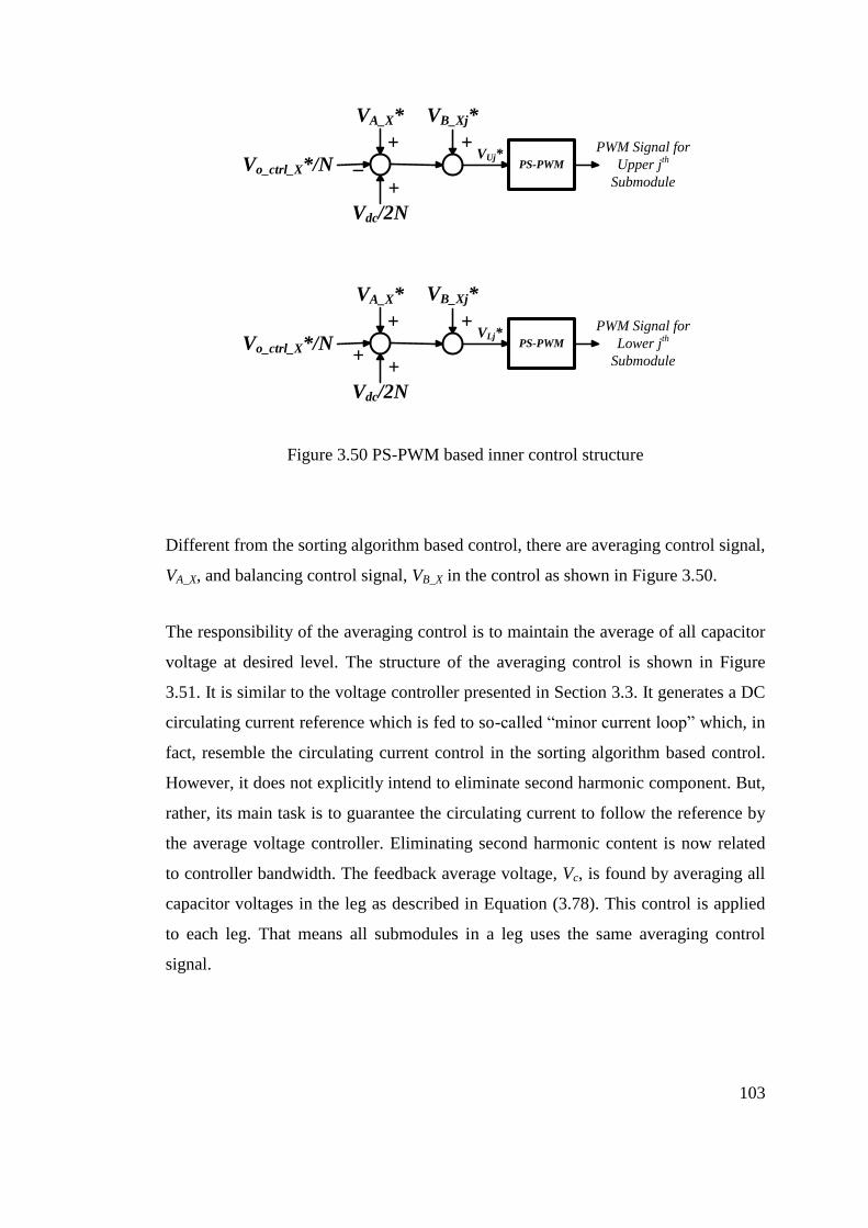
103
_Vo_ctrl_X*/N
VA_X*
+
+PS-PWM
PWM Signal for
Upper jth
Submodule
VUj*
Vdc/2N
+
VB_Xj*
+Vo_ctrl_X*/N
VA_X*
+
+PS-PWM
PWM Signal for
Lower jth
Submodule
VLj*
Vdc/2N
+
VB_Xj*
Figure 3.50 PS-PWM based inner control structure
Different from the sorting algorithm based control, there are averaging control signal,
VA_X, and balancing control signal, VB_X in the control as shown in Figure 3.50.
The responsibility of the averaging control is to maintain the average of all capacitor
voltage at desired level. The structure of the averaging control is shown in Figure
3.51. It is similar to the voltage controller presented in Section 3.3. It generates a DC
circulating current reference which is fed to so-called “minor current loop” which, in
fact, resemble the circulating current control in the sorting algorithm based control.
However, it does not explicitly intend to eliminate second harmonic component. But,
rather, its main task is to guarantee the circulating current to follow the reference by
the average voltage controller. Eliminating second harmonic content is now related
to controller bandwidth. The feedback average voltage, Vc, is found by averaging all
capacitor voltages in the leg as described in Equation (3.78). This control is applied
to each leg. That means all submodules in a leg uses the same averaging control
signal.
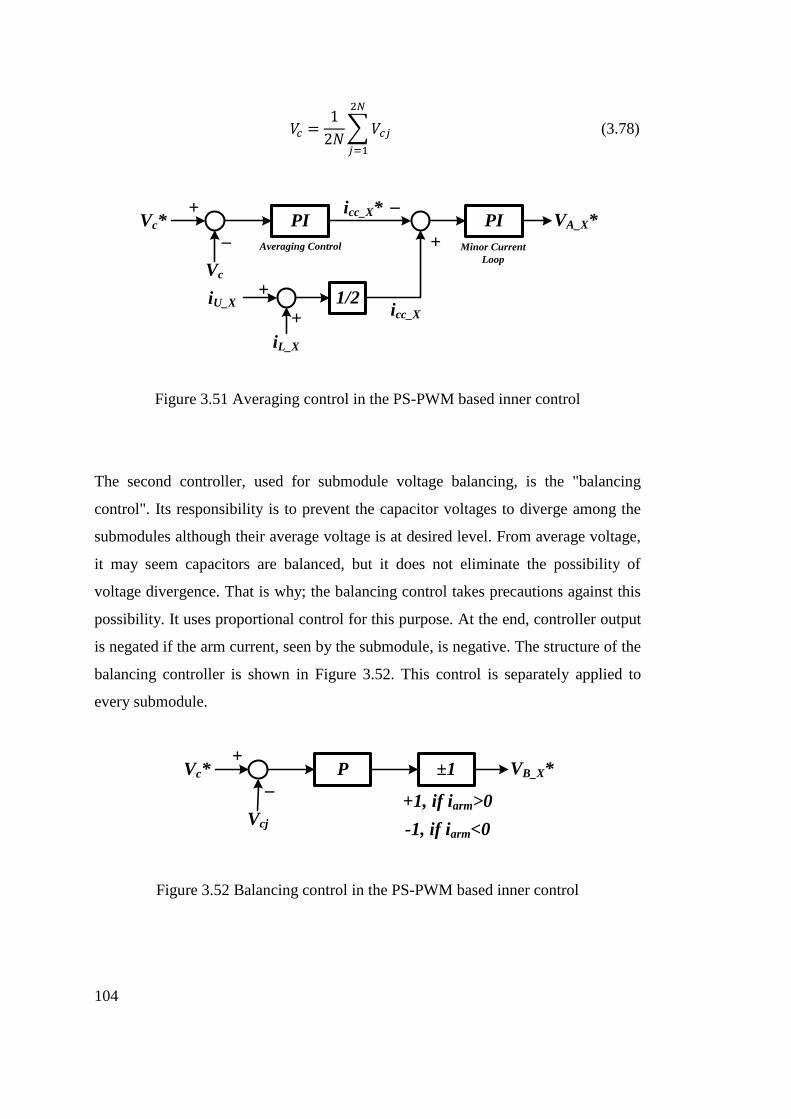
104
(3.78)
_Vc*
+
Vc
PI_
+
VA_X*
+
+iU_X
iL_X
1/2
PI
icc_X
icc_X*
Averaging Control Minor Current
Loop
Figure 3.51 Averaging control in the PS-PWM based inner control
The second controller, used for submodule voltage balancing, is the "balancing
control". Its responsibility is to prevent the capacitor voltages to diverge among the
submodules although their average voltage is at desired level. From average voltage,
it may seem capacitors are balanced, but it does not eliminate the possibility of
voltage divergence. That is why; the balancing control takes precautions against this
possibility. It uses proportional control for this purpose. At the end, controller output
is negated if the arm current, seen by the submodule, is negative. The structure of the
balancing controller is shown in Figure 3.52. This control is separately applied to
every submodule.
_Vc*
+
Vcj
P VB_X*±1
+1, if iarm>0
-1, if iarm<0
Figure 3.52 Balancing control in the PS-PWM based inner control
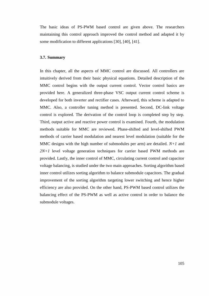
105
The basic ideas of PS-PWM based control are given above. The researchers
maintaining this control approach improved the control method and adapted it by
some modification to different applications [30], [40], [41].
3.7. Summary
In this chapter, all the aspects of MMC control are discussed. All controllers are
intuitively derived from their basic physical equations. Detailed description of the
MMC control begins with the output current control. Vector control basics are
provided here. A generalized three-phase VSC output current control scheme is
developed for both inverter and rectifier cases. Afterward, this scheme is adapted to
MMC. Also, a controller tuning method is presented. Second, DC-link voltage
control is explored. The derivation of the control loop is completed step by step.
Third, output active and reactive power control is examined. Fourth, the modulation
methods suitable for MMC are reviewed. Phase-shifted and level-shifted PWM
methods of carrier based modulation and nearest level modulation (suitable for the
MMC designs with the high number of submodules per arm) are detailed. N+1 and
2N+1 level voltage generation techniques for carrier based PWM methods are
provided. Lastly, the inner control of MMC, circulating current control and capacitor
voltage balancing, is studied under the two main approaches. Sorting algorithm based
inner control utilizes sorting algorithm to balance submodule capacitors. The gradual
improvement of the sorting algorithm targeting lower switching and hence higher
efficiency are also provided. On the other hand, PS-PWM based control utilizes the
balancing effect of the PS-PWM as well as active control in order to balance the
submodule voltages.

106
107
CHAPTER 4
4. ASSESSMENT OF CONTROL AND SWITCHING METHODS
ON A DC/AC MMC
ASSESSMENT OF CONTROL AND SWITCHING METHODS ON
A DC/AC MMC
4.1. Introduction
The control aspects of MMC are studied in Chapter 3. The application of these
control rules on a sample MMC is presented in this chapter. First of all, on a basic
DC/AC MMC, several characteristic electrical parameters under steady-state and
dynamic operating conditions are visualized. Later, the control rules such as
circulating current control, sorting algorithm, and modulation methods are applied
and their effects are observed. The aim of this part is to understand the behavior of
MMC by observing the converter responses to various control and modulation
methods.
4.2. Basic DC/AC MMC
On an example MMC system shown in Figure 4.1, load and circulating current
control, PWM, and submodule capacitor voltage balancing are realized with
MATLAB/Simulink [42] simulation. The 10-MVA MMC system is connected to 6-
kV medium voltage grid.
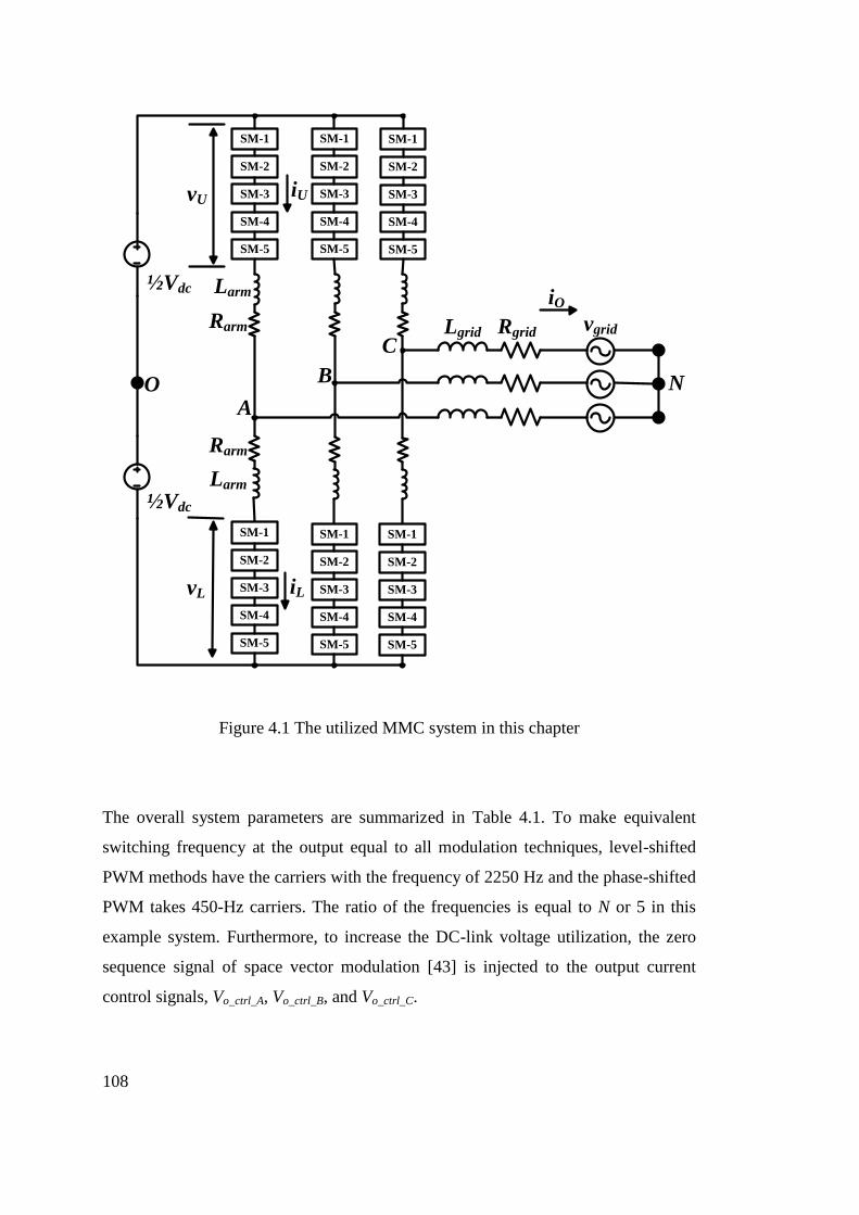
108
SM-1
SM-2
SM-3
Larm
Rarm Rgrid vgrid
NO
iO
vUiU
Lgrid
Rarm
Larm
½Vdc
½Vdc
SM-4
SM-5
SM-1
SM-2
SM-3vL
SM-4
SM-5
iL
SM-1
SM-2
SM-3
SM-4
SM-5
SM-1
SM-2
SM-3
SM-4
SM-5
SM-1
SM-2
SM-3
SM-4
SM-5
SM-1
SM-2
SM-3
SM-4
SM-5
A
B
C
Figure 4.1 The utilized MMC system in this chapter
The overall system parameters are summarized in Table 4.1. To make equivalent
switching frequency at the output equal to all modulation techniques, level-shifted
PWM methods have the carriers with the frequency of 2250 Hz and the phase-shifted
PWM takes 450-Hz carriers. The ratio of the frequencies is equal to N or 5 in this
example system. Furthermore, to increase the DC-link voltage utilization, the zero
sequence signal of space vector modulation [43] is injected to the output current
control signals, Vo_ctrl_A, Vo_ctrl_B, and Vo_ctrl_C.

109
Table 4.1 DC/AC MMC system properties
Symbol Meaning Value Unit Comment
S Power 10 MVA
N Submodules per arm 5 -
fc PWM carrier frequency 2250
Hz Level-shifted PWM
450 Phase-shifted PWM
VDC DC-link voltage 10 kV
Rarm Arm equivalent resistance 50 mΩ
Larm Arm inductance 2.5 mH 0.225 pu
CSM Submodule capacitance 6 mF 36 kJ/MVA
Vgrid Grid voltage (line-to-line) 6 kV
Rgrid Grid equivalent resistance 24 mΩ
Lgrid Grid equivalent inductance 1.1 mH 0.1 pu
f Grid frequency 50 Hz
The overall control system used in this chapter is shown in Figure 4.2 where the
inside of the blocks are already detailed in Chapter 3. Since the DC-link is stiff
voltage source, the power controller is used.
– /+
VDC /2
Vo_ctrl*
Vcc_ctrl*
+
PWM
Gate
SignalsSORTING
ALGORITHM
NonVU/L*OUTPUT
CURRENT
CONTROL
Q*
CIRCULATING
CURRENT
CONTROL
–
Icc_q2*=0
Seperate for each arm
POWER
CONTROL
Icc_d2*=0
Io_q*
MMC
PLLθe & ωe
Ed & Eq
VSM
Io_q Io_q
IU/L
P*POWER
CONTROL
Io_d*
Current
FeedbackIo_q & Io_qArm
Currents
Icc_d2
Icc_q2
Icc_d2 & Icc_q2
Figure 4.2 Overall MMC control structure
In Appendix, the pictures from the MMC simulation on MATLAB/Simulink
software are given to better illustrate the implementation in this chapter.
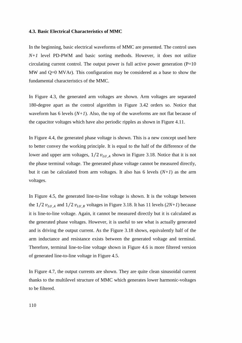
110
4.3. Basic Electrical Characteristics of MMC
In the beginning, basic electrical waveforms of MMC are presented. The control uses
N+1 level PD-PWM and basic sorting methods. However, it does not utilize
circulating current control. The output power is full active power generation (P=10
MW and Q=0 MVAr). This configuration may be considered as a base to show the
fundamental characteristics of the MMC.
In Figure 4.3, the generated arm voltages are shown. Arm voltages are separated
180-degree apart as the control algorithm in Figure 3.42 orders so. Notice that
waveform has 6 levels (N+1). Also, the top of the waveforms are not flat because of
the capacitor voltages which have also periodic ripples as shown in Figure 4.11.
In Figure 4.4, the generated phase voltage is shown. This is a new concept used here
to better convey the working principle. It is equal to the half of the difference of the
lower and upper arm voltages, shown in Figure 3.18. Notice that it is not
the phase terminal voltage. The generated phase voltage cannot be measured directly,
but it can be calculated from arm voltages. It also has 6 levels (N+1) as the arm
voltages.
In Figure 4.5, the generated line-to-line voltage is shown. It is the voltage between
the and voltages in Figure 3.18. It has 11 levels (2N+1) because
it is line-to-line voltage. Again, it cannot be measured directly but it is calculated as
the generated phase voltages. However, it is useful to see what is actually generated
and is driving the output current. As the Figure 3.18 shows, equivalently half of the
arm inductance and resistance exists between the generated voltage and terminal.
Therefore, terminal line-to-line voltage shown in Figure 4.6 is more filtered version
of generated line-to-line voltage in Figure 4.5.
In Figure 4.7, the output currents are shown. They are quite clean sinusoidal current
thanks to the multilevel structure of MMC which generates lower harmonic-voltages
to be filtered.
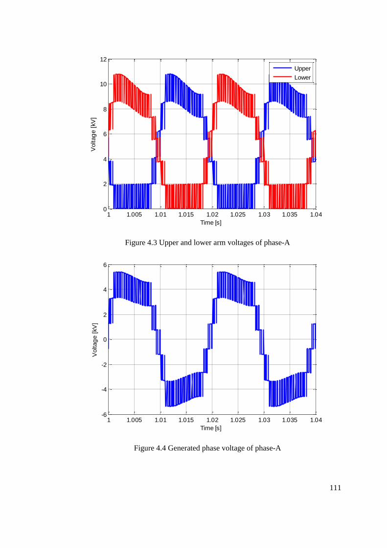
111
Figure 4.3 Upper and lower arm voltages of phase-A
Figure 4.4 Generated phase voltage of phase-A
1 1.005 1.01 1.015 1.02 1.025 1.03 1.035 1.040
2
4
6
8
10
12
Time [s]
Voltag
e [
kV]
Upper
Lower
1 1.005 1.01 1.015 1.02 1.025 1.03 1.035 1.04-6
-4
-2
0
2
4
6
Time [s]
Voltag
e [
kV]
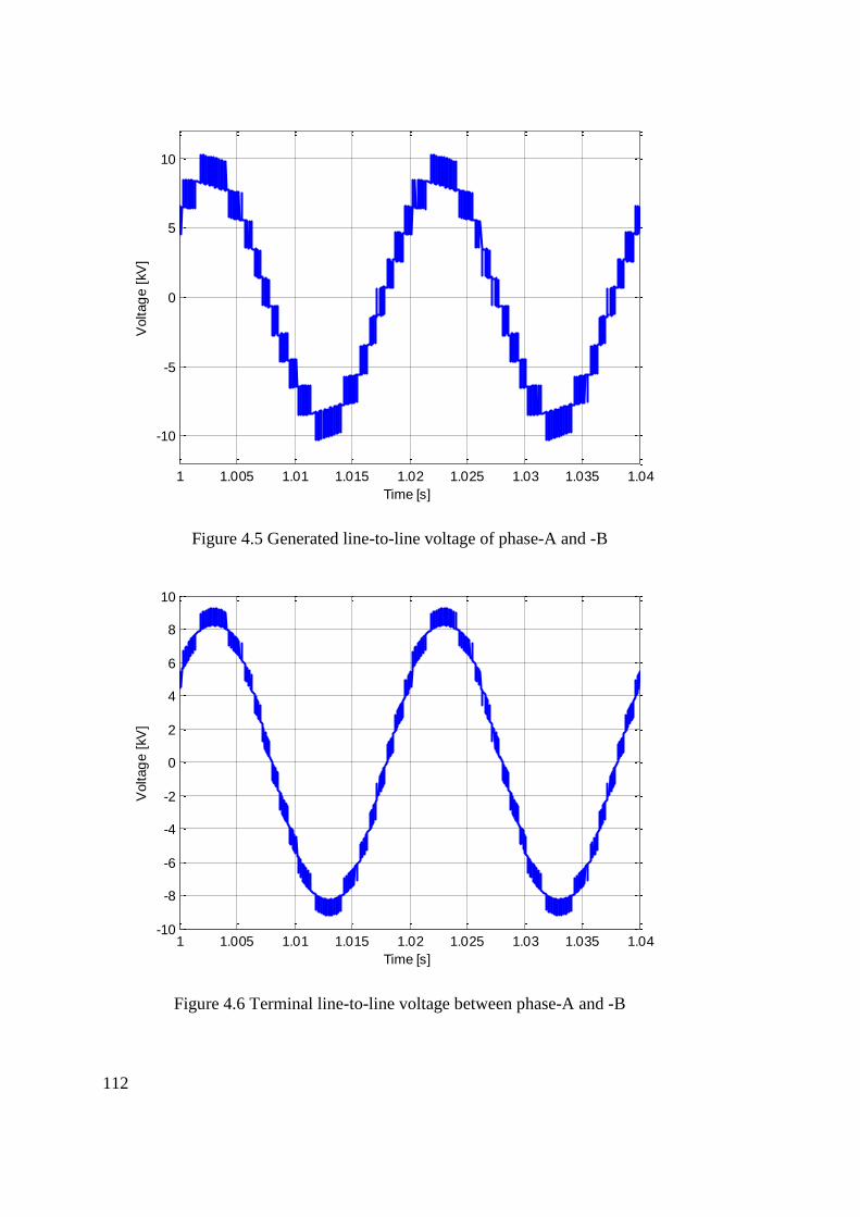
112
Figure 4.5 Generated line-to-line voltage of phase-A and -B
Figure 4.6 Terminal line-to-line voltage between phase-A and -B
1 1.005 1.01 1.015 1.02 1.025 1.03 1.035 1.04
-10
-5
0
5
10
Time [s]
Voltag
e [
kV]
1 1.005 1.01 1.015 1.02 1.025 1.03 1.035 1.04-10
-8
-6
-4
-2
0
2
4
6
8
10
Time [s]
Voltag
e [
kV]
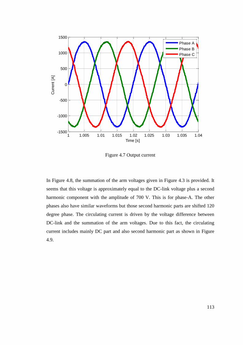
113
Figure 4.7 Output current
In Figure 4.8, the summation of the arm voltages given in Figure 4.3 is provided. It
seems that this voltage is approximately equal to the DC-link voltage plus a second
harmonic component with the amplitude of 700 V. This is for phase-A. The other
phases also have similar waveforms but those second harmonic parts are shifted 120
degree phase. The circulating current is driven by the voltage difference between
DC-link and the summation of the arm voltages. Due to this fact, the circulating
current includes mainly DC part and also second harmonic part as shown in Figure
4.9.
1 1.005 1.01 1.015 1.02 1.025 1.03 1.035 1.04-1500
-1000
-500
0
500
1000
1500
Time [s]
Curr
ent
[A]
Phase A
Phase B
Phase C
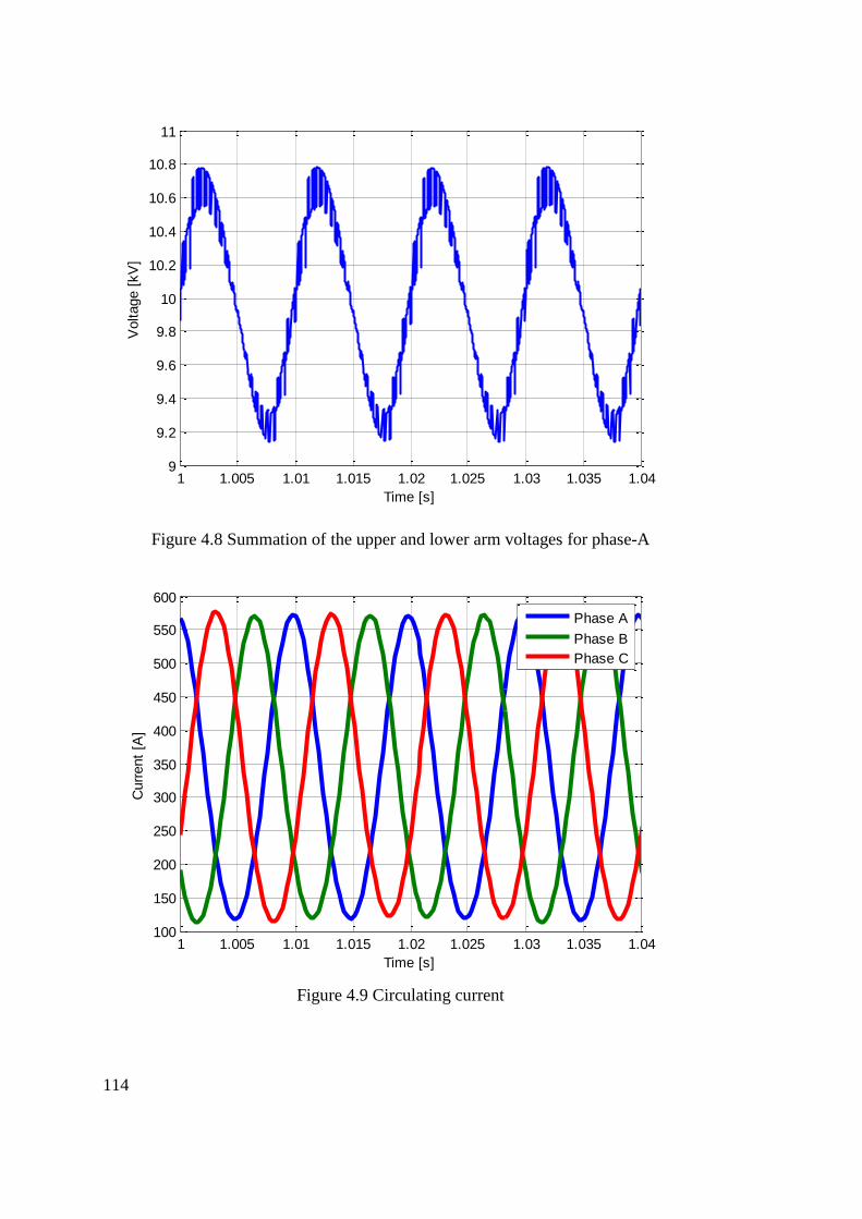
114
Figure 4.8 Summation of the upper and lower arm voltages for phase-A
Figure 4.9 Circulating current
1 1.005 1.01 1.015 1.02 1.025 1.03 1.035 1.049
9.2
9.4
9.6
9.8
10
10.2
10.4
10.6
10.8
11
Time [s]
Voltage [
kV
]
1 1.005 1.01 1.015 1.02 1.025 1.03 1.035 1.04100
150
200
250
300
350
400
450
500
550
600
Time [s]
Curr
ent
[A]
Phase A
Phase B
Phase C
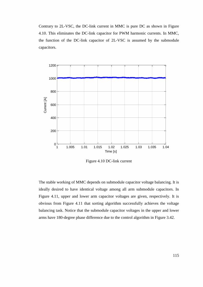
115
Contrary to 2L-VSC, the DC-link current in MMC is pure DC as shown in Figure
4.10. This eliminates the DC-link capacitor for PWM harmonic currents. In MMC,
the function of the DC-link capacitor of 2L-VSC is assumed by the submodule
capacitors.
Figure 4.10 DC-link current
The stable working of MMC depends on submodule capacitor voltage balancing. It is
ideally desired to have identical voltage among all arm submodule capacitors. In
Figure 4.11, upper and lower arm capacitor voltages are given, respectively. It is
obvious from Figure 4.11 that sorting algorithm successfully achieves the voltage
balancing task. Notice that the submodule capacitor voltages in the upper and lower
arms have 180-degree phase difference due to the control algorithm in Figure 3.42.
1 1.005 1.01 1.015 1.02 1.025 1.03 1.035 1.040
200
400
600
800
1000
1200
Time [s]
Curr
ent
[A]
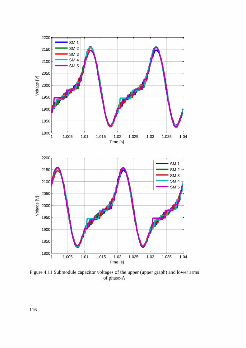
116
Figure 4.11 Submodule capacitor voltages of the upper (upper graph) and lower arms
of phase-A
1 1.005 1.01 1.015 1.02 1.025 1.03 1.035 1.041800
1850
1900
1950
2000
2050
2100
2150
2200
Time [s]
Voltage [
V]
SM 1
SM 2
SM 3
SM 4
SM 5
1 1.005 1.01 1.015 1.02 1.025 1.03 1.035 1.041800
1850
1900
1950
2000
2050
2100
2150
2200
Time [s]
Voltage [
V]
SM 1
SM 2
SM 3
SM 4
SM 5
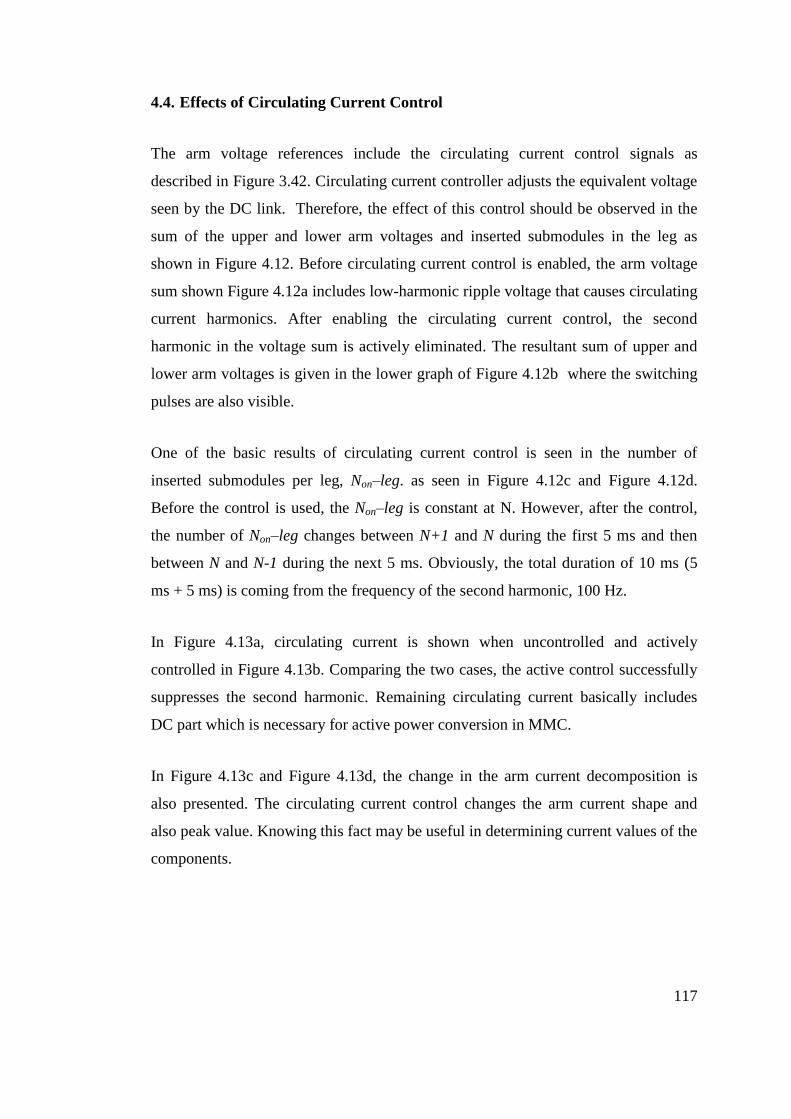
117
4.4. Effects of Circulating Current Control
The arm voltage references include the circulating current control signals as
described in Figure 3.42. Circulating current controller adjusts the equivalent voltage
seen by the DC link. Therefore, the effect of this control should be observed in the
sum of the upper and lower arm voltages and inserted submodules in the leg as
shown in Figure 4.12. Before circulating current control is enabled, the arm voltage
sum shown Figure 4.12a includes low-harmonic ripple voltage that causes circulating
current harmonics. After enabling the circulating current control, the second
harmonic in the voltage sum is actively eliminated. The resultant sum of upper and
lower arm voltages is given in the lower graph of Figure 4.12b where the switching
pulses are also visible.
One of the basic results of circulating current control is seen in the number of
inserted submodules per leg, Non–leg. as seen in Figure 4.12c and Figure 4.12d.
Before the control is used, the Non–leg is constant at N. However, after the control,
the number of Non–leg changes between N+1 and N during the first 5 ms and then
between N and N-1 during the next 5 ms. Obviously, the total duration of 10 ms (5
ms + 5 ms) is coming from the frequency of the second harmonic, 100 Hz.
In Figure 4.13a, circulating current is shown when uncontrolled and actively
controlled in Figure 4.13b. Comparing the two cases, the active control successfully
suppresses the second harmonic. Remaining circulating current basically includes
DC part which is necessary for active power conversion in MMC.
In Figure 4.13c and Figure 4.13d, the change in the arm current decomposition is
also presented. The circulating current control changes the arm current shape and
also peak value. Knowing this fact may be useful in determining current values of the
components.

118
(a) Sum of upper and lower arm voltage: Uncontrolled circulating current
(b) Sum of upper and lower arm voltage: Controlled circulating current
(c) Inserted submodules in the leg: Uncontrolled circulating current
(d) Inserted submodules in the leg: Controlled circulating current
Figure 4.12 Effects of circulating current control on arm voltages
1 1.005 1.01 1.015 1.02 1.025 1.03 1.035 1.047
8
9
10
11
12
13
Time [s]
Vo
lta
ge
[kV
]
1 1.005 1.01 1.015 1.02 1.025 1.03 1.035 1.047
8
9
10
11
12
13
Vo
lta
ge
[kV
]
1 1.005 1.01 1.015 1.02 1.025 1.03 1.035 1.040
1
2
3
4
5
6
Time [s]
No
n -
leg
1 1.005 1.01 1.015 1.02 1.025 1.03 1.035 1.040
1
2
3
4
5
6
7
Time [s]
No
n -
leg
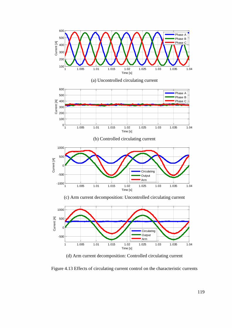
119
(a) Uncontrolled circulating current
(b) Controlled circulating current
(c) Arm current decomposition: Uncontrolled circulating current
(d) Arm current decomposition: Controlled circulating current
Figure 4.13 Effects of circulating current control on the characteristic currents
1 1.005 1.01 1.015 1.02 1.025 1.03 1.035 1.04100
200
300
400
500
600
Time [s]
Cu
rre
nt
[A]
Phase A
Phase B
Phase C
1 1.005 1.01 1.015 1.02 1.025 1.03 1.035 1.040
100
200
300
400
500
600
Time [s]
Cu
rre
nt
[A]
Phase A
Phase B
Phase C
1 1.005 1.01 1.015 1.02 1.025 1.03 1.035 1.04-1000
-500
0
500
1000
Time [s]
Cu
rre
nt
[A]
Circulating
Output
Arm
1 1.005 1.01 1.015 1.02 1.025 1.03 1.035 1.04
-500
0
500
1000
Time [s]
Cu
rre
nt
[A]
Circulating
Output
Arm
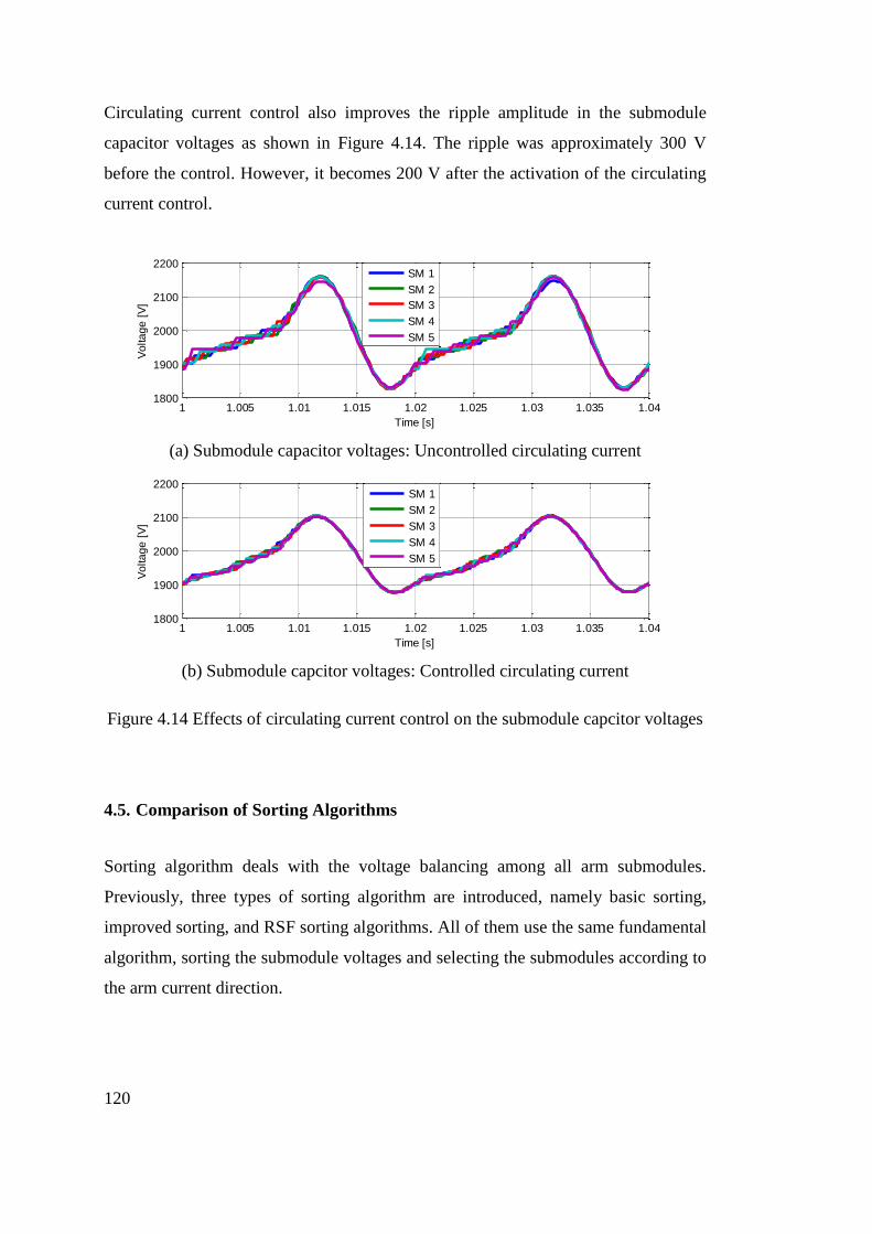
120
Circulating current control also improves the ripple amplitude in the submodule
capacitor voltages as shown in Figure 4.14. The ripple was approximately 300 V
before the control. However, it becomes 200 V after the activation of the circulating
current control.
(a) Submodule capacitor voltages: Uncontrolled circulating current
(b) Submodule capcitor voltages: Controlled circulating current
Figure 4.14 Effects of circulating current control on the submodule capcitor voltages
4.5. Comparison of Sorting Algorithms
Sorting algorithm deals with the voltage balancing among all arm submodules.
Previously, three types of sorting algorithm are introduced, namely basic sorting,
improved sorting, and RSF sorting algorithms. All of them use the same fundamental
algorithm, sorting the submodule voltages and selecting the submodules according to
the arm current direction.
1 1.005 1.01 1.015 1.02 1.025 1.03 1.035 1.041800
1900
2000
2100
2200
Time [s]
Vo
lta
ge
[V
]
SM 1
SM 2
SM 3
SM 4
SM 5
1 1.005 1.01 1.015 1.02 1.025 1.03 1.035 1.041800
1900
2000
2100
2200
Time [s]
Vo
lta
ge
[V
]
SM 1
SM 2
SM 3
SM 4
SM 5
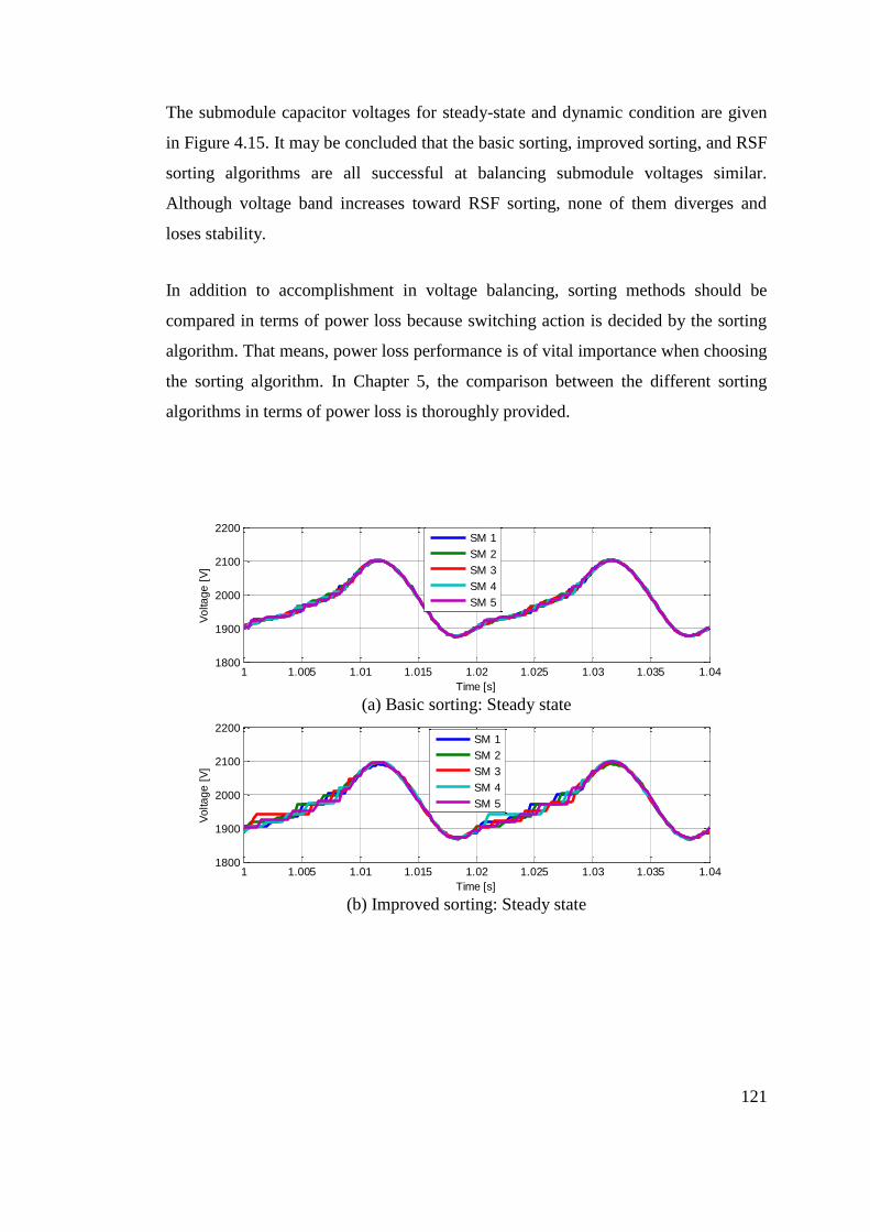
121
The submodule capacitor voltages for steady-state and dynamic condition are given
in Figure 4.15. It may be concluded that the basic sorting, improved sorting, and RSF
sorting algorithms are all successful at balancing submodule voltages similar.
Although voltage band increases toward RSF sorting, none of them diverges and
loses stability.
In addition to accomplishment in voltage balancing, sorting methods should be
compared in terms of power loss because switching action is decided by the sorting
algorithm. That means, power loss performance is of vital importance when choosing
the sorting algorithm. In Chapter 5, the comparison between the different sorting
algorithms in terms of power loss is thoroughly provided.
(a) Basic sorting: Steady state
(b) Improved sorting: Steady state
1 1.005 1.01 1.015 1.02 1.025 1.03 1.035 1.041800
1900
2000
2100
2200
Time [s]
Vo
lta
ge
[V
]
SM 1
SM 2
SM 3
SM 4
SM 5
1 1.005 1.01 1.015 1.02 1.025 1.03 1.035 1.041800
1900
2000
2100
2200
Time [s]
Vo
lta
ge
[V
]
SM 1
SM 2
SM 3
SM 4
SM 5
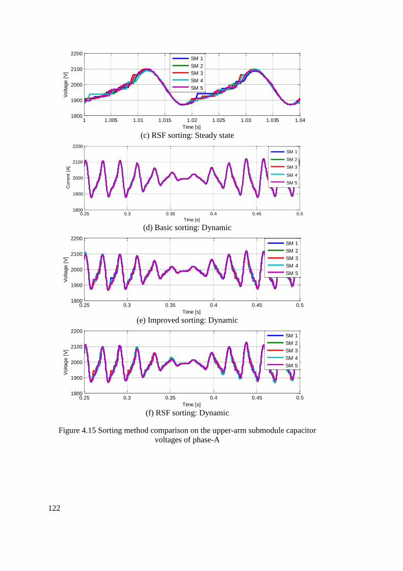
122
(c) RSF sorting: Steady state
(d) Basic sorting: Dynamic
(e) Improved sorting: Dynamic
(f) RSF sorting: Dynamic
Figure 4.15 Sorting method comparison on the upper-arm submodule capacitor
voltages of phase-A
1 1.005 1.01 1.015 1.02 1.025 1.03 1.035 1.041800
1900
2000
2100
2200
Time [s]
Vo
lta
ge
[V
]
SM 1
SM 2
SM 3
SM 4
SM 5
0.25 0.3 0.35 0.4 0.45 0.51800
1900
2000
2100
2200
Time [s]
Cu
rre
nt
[A]
SM 1
SM 2
SM 3
SM 4
SM 5
0.25 0.3 0.35 0.4 0.45 0.51800
1900
2000
2100
2200
Time [s]
Vo
lta
ge
[V
]
SM 1
SM 2
SM 3
SM 4
SM 5
0.25 0.3 0.35 0.4 0.45 0.51800
1900
2000
2100
2200
Time [s]
Vo
lta
ge
[V
]
SM 1
SM 2
SM 3
SM 4
SM 5
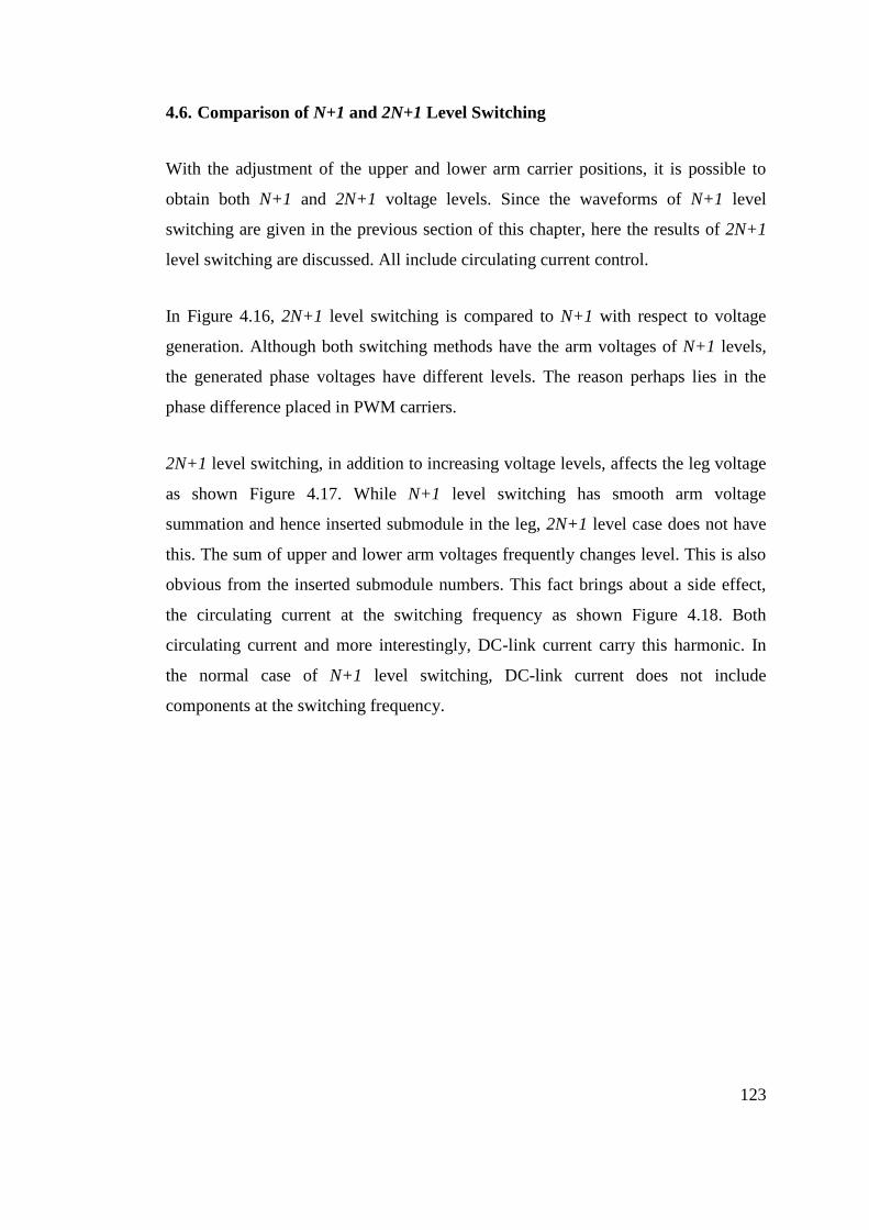
123
4.6. Comparison of N+1 and 2N+1 Level Switching
With the adjustment of the upper and lower arm carrier positions, it is possible to
obtain both N+1 and 2N+1 voltage levels. Since the waveforms of N+1 level
switching are given in the previous section of this chapter, here the results of 2N+1
level switching are discussed. All include circulating current control.
In Figure 4.16, 2N+1 level switching is compared to N+1 with respect to voltage
generation. Although both switching methods have the arm voltages of N+1 levels,
the generated phase voltages have different levels. The reason perhaps lies in the
phase difference placed in PWM carriers.
2N+1 level switching, in addition to increasing voltage levels, affects the leg voltage
as shown Figure 4.17. While N+1 level switching has smooth arm voltage
summation and hence inserted submodule in the leg, 2N+1 level case does not have
this. The sum of upper and lower arm voltages frequently changes level. This is also
obvious from the inserted submodule numbers. This fact brings about a side effect,
the circulating current at the switching frequency as shown Figure 4.18. Both
circulating current and more interestingly, DC-link current carry this harmonic. In
the normal case of N+1 level switching, DC-link current does not include
components at the switching frequency.

124
(a) Arm voltages of phase-A: N+1 level switching
(b) Arm voltages of phase-A: 2N+1 level switching
(c) Generated phase-A voltage: N+1 level switching
(d) Generated phase-A voltage: 2N+1 level switching
Figure 4.16 Effects of 2N+1 level switching on voltage generation
1 1.005 1.01 1.015 1.02 1.025 1.03 1.035 1.040
2
4
6
8
10
12
Time [s]
Vo
lta
ge
[kV
]
Upper
Lower
1 1.005 1.01 1.015 1.02 1.025 1.03 1.035 1.040
2
4
6
8
10
12
Time [s]
Vo
lta
ge
[kV
]
Upper
Lower
1 1.005 1.01 1.015 1.02 1.025 1.03 1.035 1.04-6
-4
-2
0
2
4
6
Time [s]
Vo
lta
ge
[kV
]
1 1.005 1.01 1.015 1.02 1.025 1.03 1.035 1.04-6
-4
-2
0
2
4
6
Time [s]
Vo
lta
ge
[kV
]
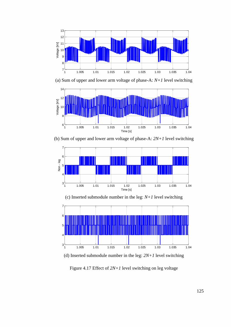
125
(a) Sum of upper and lower arm voltage of phase-A: N+1 level switching
(b) Sum of upper and lower arm voltage of phase-A: 2N+1 level switching
(c) Inserted submodule number in the leg: N+1 level switching
(d) Inserted submodule number in the leg: 2N+1 level switching
Figure 4.17 Effect of 2N+1 level switching on leg voltage
1 1.005 1.01 1.015 1.02 1.025 1.03 1.035 1.047
8
9
10
11
12
13
Vo
lta
ge
[kV
]
1 1.005 1.01 1.015 1.02 1.025 1.03 1.035 1.046
8
10
12
14
Time [s]
Vo
lta
ge
[kV
]
1 1.005 1.01 1.015 1.02 1.025 1.03 1.035 1.043
4
5
6
7
Time [s]
No
n -
leg
1 1.005 1.01 1.015 1.02 1.025 1.03 1.035 1.043
4
5
6
7
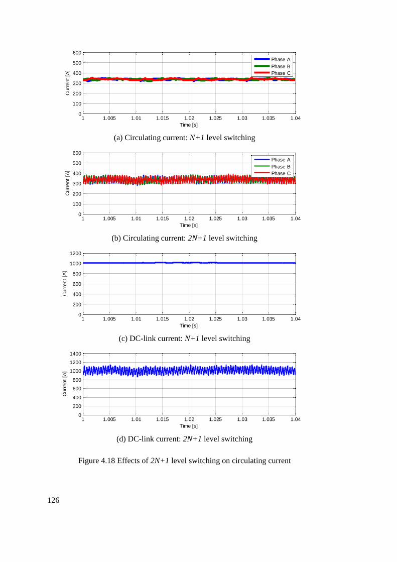
126
(a) Circulating current: N+1 level switching
(b) Circulating current: 2N+1 level switching
(c) DC-link current: N+1 level switching
(d) DC-link current: 2N+1 level switching
Figure 4.18 Effects of 2N+1 level switching on circulating current
1 1.005 1.01 1.015 1.02 1.025 1.03 1.035 1.040
100
200
300
400
500
600
Time [s]
Cu
rre
nt
[A]
Phase A
Phase B
Phase C
1 1.005 1.01 1.015 1.02 1.025 1.03 1.035 1.040
100
200
300
400
500
600
Time [s]
Cu
rre
nt
[A]
Phase A
Phase B
Phase C
1 1.005 1.01 1.015 1.02 1.025 1.03 1.035 1.040
200
400
600
800
1000
1200
Time [s]
Cu
rre
nt
[A]
1 1.005 1.01 1.015 1.02 1.025 1.03 1.035 1.040
200
400
600
800
1000
1200
1400
Time [s]
Cu
rre
nt
[A]
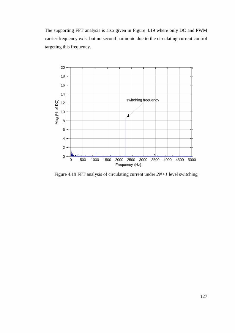
127
The supporting FFT analysis is also given in Figure 4.19 where only DC and PWM
carrier frequency exist but no second harmonic due to the circulating current control
targeting this frequency.
Figure 4.19 FFT analysis of circulating current under 2N+1 level switching
0 500 1000 1500 2000 2500 3000 3500 4000 4500 50000
2
4
6
8
10
12
14
16
18
20
Frequency (Hz)
Mag (
% o
f D
C) switching frequency
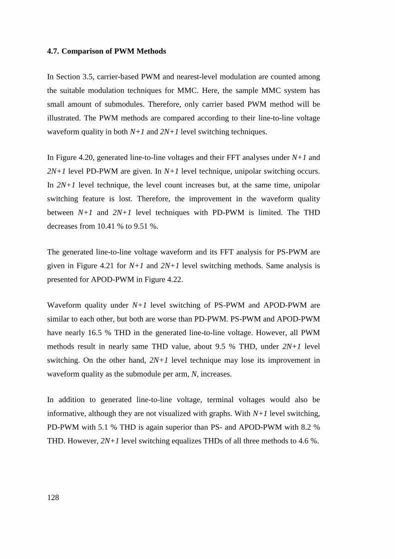
128
4.7. Comparison of PWM Methods
In Section 3.5, carrier-based PWM and nearest-level modulation are counted among
the suitable modulation techniques for MMC. Here, the sample MMC system has
small amount of submodules. Therefore, only carrier based PWM method will be
illustrated. The PWM methods are compared according to their line-to-line voltage
waveform quality in both N+1 and 2N+1 level switching techniques.
In Figure 4.20, generated line-to-line voltages and their FFT analyses under N+1 and
2N+1 level PD-PWM are given. In N+1 level technique, unipolar switching occurs.
In 2N+1 level technique, the level count increases but, at the same time, unipolar
switching feature is lost. Therefore, the improvement in the waveform quality
between N+1 and 2N+1 level techniques with PD-PWM is limited. The THD
decreases from 10.41 % to 9.51 %.
The generated line-to-line voltage waveform and its FFT analysis for PS-PWM are
given in Figure 4.21 for N+1 and 2N+1 level switching methods. Same analysis is
presented for APOD-PWM in Figure 4.22.
Waveform quality under N+1 level switching of PS-PWM and APOD-PWM are
similar to each other, but both are worse than PD-PWM. PS-PWM and APOD-PWM
have nearly 16.5 % THD in the generated line-to-line voltage. However, all PWM
methods result in nearly same THD value, about 9.5 % THD, under 2N+1 level
switching. On the other hand, 2N+1 level technique may lose its improvement in
waveform quality as the submodule per arm, N, increases.
In addition to generated line-to-line voltage, terminal voltages would also be
informative, although they are not visualized with graphs. With N+1 level switching,
PD-PWM with 5.1 % THD is again superior than PS- and APOD-PWM with 8.2 %
THD. However, 2N+1 level switching equalizes THDs of all three methods to 4.6 %.
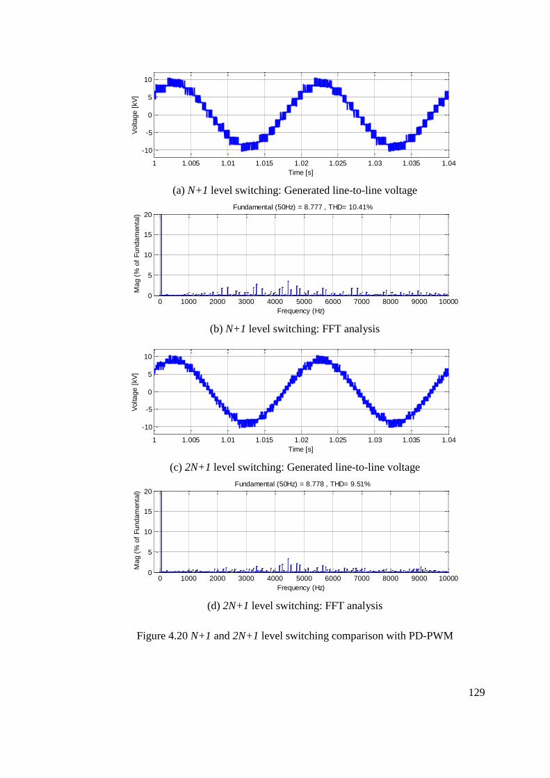
129
(a) N+1 level switching: Generated line-to-line voltage
(b) N+1 level switching: FFT analysis
(c) 2N+1 level switching: Generated line-to-line voltage
(d) 2N+1 level switching: FFT analysis
Figure 4.20 N+1 and 2N+1 level switching comparison with PD-PWM
1 1.005 1.01 1.015 1.02 1.025 1.03 1.035 1.04
-10
-5
0
5
10
Time [s]
Vo
lta
ge
[kV
]
0 1000 2000 3000 4000 5000 6000 7000 8000 9000 100000
5
10
15
20
Frequency (Hz)
Fundamental (50Hz) = 8.777 , THD= 10.41%
Ma
g (
% o
f F
un
da
men
tal)
1 1.005 1.01 1.015 1.02 1.025 1.03 1.035 1.04
-10
-5
0
5
10
Time [s]
Vo
lta
ge
[kV
]
0 1000 2000 3000 4000 5000 6000 7000 8000 9000 100000
5
10
15
20
Frequency (Hz)
Fundamental (50Hz) = 8.778 , THD= 9.51%
Ma
g (
% o
f F
un
da
men
tal)
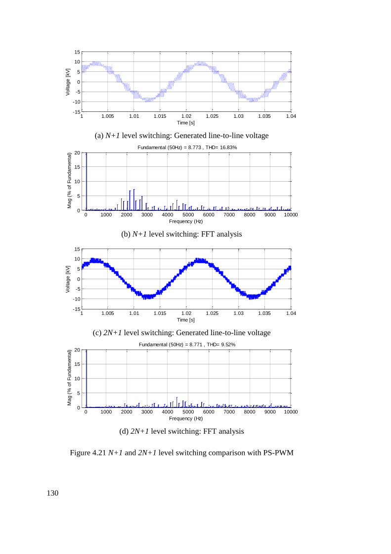
130
(a) N+1 level switching: Generated line-to-line voltage
(b) N+1 level switching: FFT analysis
(c) 2N+1 level switching: Generated line-to-line voltage
(d) 2N+1 level switching: FFT analysis
Figure 4.21 N+1 and 2N+1 level switching comparison with PS-PWM
1 1.005 1.01 1.015 1.02 1.025 1.03 1.035 1.04-15
-10
-5
0
5
10
15
Time [s]
Vo
lta
ge
[kV
]
0 1000 2000 3000 4000 5000 6000 7000 8000 9000 100000
5
10
15
20
Frequency (Hz)
Fundamental (50Hz) = 8.773 , THD= 16.83%
Ma
g (
% o
f F
un
da
men
tal)
1 1.005 1.01 1.015 1.02 1.025 1.03 1.035 1.04-15
-10
-5
0
5
10
15
Time [s]
Vo
lta
ge
[kV
]
0 1000 2000 3000 4000 5000 6000 7000 8000 9000 100000
5
10
15
20
Frequency (Hz)
Fundamental (50Hz) = 8.771 , THD= 9.52%
Ma
g (
% o
f F
un
da
men
tal)
131
(a) N+1 level switching: Generated line-to-line voltage
(b) N+1 level switching: FFT analysis
(c) 2N+1 level switching: Generated line-to-line voltage
(d) 2N+1 level switching: FFT analysis
Figure 4.22 N+1 and 2N+1 level switching comparison with APOD-PWM
1 1.005 1.01 1.015 1.02 1.025 1.03 1.035 1.04-15
-10
-5
0
5
10
15
Time [s]
vo
lta
ge
[kV
]
0 1000 2000 3000 4000 5000 6000 7000 8000 9000 100000
5
10
15
20
Frequency (Hz)
Fundamental (50Hz) = 8.777 , THD= 16.49%
Ma
g (
% o
f F
un
da
men
tal)
1 1.005 1.01 1.015 1.02 1.025 1.03 1.035 1.04-15
-10
-5
0
5
10
15
Time [s]
Vo
lta
ge
[kV
]
0 1000 2000 3000 4000 5000 6000 7000 8000 9000 100000
5
10
15
20
Frequency (Hz)
Fundamental (50Hz) = 8.776 , THD= 9.44%
Ma
g (
% o
f F
un
da
men
tal)
132
4.8. Summary
In this chapter, the control rules and modulation techniques developed in Chapter 3
are applied to a sample MMC system and their effects are investigated.
The circulating current control suppresses the second-harmonic component. The
reason is to improve efficiency. The circulating current control directly changes the
arm current. Therefore, the commutated current in the semiconductors and also
capacitor current are all affected. As a result, capacitor voltage ripple decreases and
the efficiency improves (to be shown in Chapter 5). On the other hand, this control
does not basically affect the output side of MMC.
In this thesis, three sorting algorithms, basic sorting, improved sorting, and RSF
sorting algorithms, are listed with each having gradual improvement. In the core of
these algorithms, sorting the submodule voltages and then selecting the submodules
according to the arm current direction. Although these methods cause slightly
different voltage bands due to different switching number, they are all successful at
balancing the submodule capacitor voltages in both steady-state and dynamic
operation. That means three of them are satisfactory in electrical point of view.
However, they are proposed to improve efficiency. That being said, this chapter is
allocated to investigate electrical parameters. Therefore, in Chapter 5, the
comparison between the three sorting algorithms in terms of power loss is provided.
After the comparison of N+1 and 2N+1 level switching techniques, it is concluded
that the latter technique improves waveform quality by carrying equivalent switching
frequency at the output to two multiples of the previous one. On the other hand, some
amount of circulating current at the equivalent PWM carrier frequency is generated
although second-harmonic component of circulating current is eliminated. Similarly,
the DC-link current also include this harmonic component also.
In PWM part, N+1 and 2N+1 level switching techniques of three PWM methods,
PD-, PS-, and APOD-PWM, are compared. In the comparison, the generated and
133
terminal line-to-line voltages are used in the comparison. If N+1 level switching
technique is selected, then best methods in terms of waveform quality is PD-PWM.
The PS- and APOD-PWM methods are worse than PD-PWM in terms of waveform
quality. On the other hand, under 2N+1 level switching technique, all methods have
same lower THD level in both voltage measurement. It means 2N+1 level switching
improves waveform quality at the expense of creating a new circulating current at
PWM carrier frequency. It should be noticed that the improvement in PD-PWM is
limited. In addition, it may be expected that 2N+1 level technique may lose its
superiority in voltage waveform quality as the submodule per arm, N, increases.
Overall numerical comparison is summarized in Table 4.2. THD values of terminal
voltages are better because it is the filtered version of generated voltage by the half
of arm impedance as shown in Figure 3.18.
Table 4.2 Voltage THD comparison of PWM methods
Voltage Level PD-PWM
(%)
PS-PWM
(%)
APOD-PWM
(%)
Generated Line-to-
Line Voltage
N+1 10.4 16.5 16.5
2N+1 9.5 9.5 9.5
Terminal Line-to-
Line Voltage
N+1 5.1 8.1 8.1
2N+1 4.6 4.6 4.6

134
CHAPTER 5
5. POWER LOSS ANALYSIS OF MMC
POWER LOSS ANALYSIS OF MMC
5.1. Introduction
This chapter thoroughly examines the semiconductor power loss characteristics of
MMC. Power loss behavior is examined under different PWM methods and
operating conditions. The effects of stored energy level, circulating current control
utilization, power factor and submodule voltage balancing method on power loss are
studied. Furthermore, unbalanced power losses and specific semiconductor thermal
stresses within a submodule are visualized by investigating the loss distribution in a
submodule. The part aids in understanding and design of MMC converter modules,
selecting PWM and control methods with power loss perspective.
The design of MMC system involves some decisions such as the power
semiconductor and switching frequency selection and the passive component design.
Power loss analysis is one of the key practical issues that may affect these design
decisions. In addition, individual semiconductor thermal stresses [45] are also highly
important from the reliability perspective for such an investment.
In this chapter, the influence of the active and reactive power content of the output
current on semiconductor power loss is investigated by comparing four different
power flow cases; full active power generation (MMC system to grid) and
consumption considering the HVDC system and full reactive power generation and
consumption for the STATCOM operation.
135
The analysis also examines the influence of the circulating current and its control on
power loss under various operating conditions. It basically compares the situations
with and without circulating current control.
Multilevel PWM can be classified into two subgroups, level-shifted and phase-
shifted PWM. This study compares the prominent members of these subgroups,
phase-disposition (PD) for level-shifted PWM and phase-shifted (PS) PWM in terms
of power loss.
The sorting algorithm is used to balance the submodule capacitor voltages. The
switching actions are determined by the sorting algorithm. Therefore, switching loss
largely depends on the performance of this algorithm. An improvement to the sorting
algorithm reducing switching number without sacrificing the submodule voltage
balancing is desired. In Section 3.6, basic sorting and also improved sorting as well
as RSF sorting are defined. Here, these three approaches are compared from the
power semiconductor device power loss perspective under various operating
conditions.
The MMC system includes two passive components, namely submodule capacitor
and arm inductor. Their design is shown to be important for system control and
stability [21]. The submodule capacitance value is studied by keeping arm
inductance constant. The capacitance value can also be taken as stored energy level
(kJ/MVA) as in this work.
Furthermore, the influence of PWM carrier frequency choice on power loss is
visualized.
This chapter investigates the total system and individual semiconductor power losses
of MMC under various operating conditions and control strategies. At first, the
power loss calculation method is presented. Then, the effect of stored energy,
circulating current control, power factor and sorting algorithm on the power loss are
visualized on a 10-MVA MMC system connected to the 6-kV medium voltage grid.
136
The analysis also compares the PWM methods with power semiconductor loss
viewpoint, as an improvement of [46] which mainly studies waveform quality of the
PWM methods. At last, it focuses into unbalanced power losses within a submodule
by evaluating the loss distribution in submodules. The work in this chapter is also
summarized in [47].
5.2. Power Loss Calculation
The power loss analysis of MMC here incorporates the submodule semiconductor
power loss calculation algorithm that works alongside circuit simulation in
MATLAB/Simulink and continuously utilizes its electrical parameters. This
approach brings some key advantages such as observing loss distributions and
thermal stresses among arms and among submodules within a certain arm and among
semiconductors within a single submodule. In a commercial IGBT module, five
different loss components exist, namely IGBT conduction, turn-on, turn-off and
diode conduction and reverse recovery losses. These losses can be separated into two
subgroups and analyzed in the following manner.
5.2.1. Conduction Loss Calculation
Conduction loss is the result of voltage drop while current flows on power
semiconductor as represented in Equations (5.1) and (5.2). Because the voltage drop
is not constant but a function of the conducted current, it is represented with
polynomials as in [48] to model IGBT and diode voltage drops VCE and VF,
respectively.
(5.1)
(5.2)
Because power electronics converters are naturally based on switching action,
current flow in a semiconductor is not continuous. That is, power loss only occurs
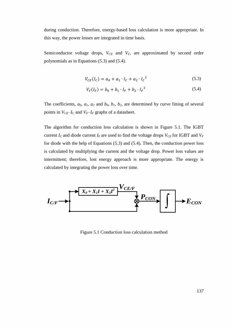
137
during conduction. Therefore, energy-based loss calculation is more appropriate. In
this way, the power losses are integrated in time basis.
Semiconductor voltage drops, VCE and VF, are approximated by second order
polynomials as in Equations (5.3) and (5.4).
(5.3)
(5.4)
The coefficients, a0, a1, a2 and b0, b1, b2, are determined by curve fitting of several
points in VCE–IC and VF–IF graphs of a datasheet.
The algorithm for conduction loss calculation is shown in Figure 5.1. The IGBT
current IC and diode current IF are used to find the voltage drops VCE for IGBT and VF
for diode with the help of Equations (5.3) and (5.4). Then, the conduction power loss
is calculated by multiplying the current and the voltage drop. Power loss values are
intermittent; therefore, lost energy approach is more appropriate. The energy is
calculated by integrating the power loss over time.
X0 + X1I + X2I2
IC/F
VCE/F
PCON
ECON
Figure 5.1 Conduction loss calculation method

138
5.2.2. Switching Loss Calculation
In real power semiconductors, current commutation cannot occur instantaneously,
and therefore, switches simultaneously experience high voltage and high current
during switching moments. This condition creates switching loss. Datasheets include
switching loss information as EON–IC for IGBT turn-on, EOFF–IC for IGBT turn-off
and EREC–IF for diode reverse recovery (turn-off) graphs. They can also be modeled
as second order polynomials as the conduction loss as in Equations (5.5), (5.6), and
(5.7). However, switching losses should be normalized with submodule capacitor
voltage because the information in datasheets is given for one specific voltage. In
this way, the datasheet values are adapted to real application conditions. VSM means
instantaneous submodule capacitor voltage whereas VNOM is the nominal test voltage
given in the datasheet.
(5.5)
(5.6)
(5.7)
The coefficients, c0, c1, c2 and d0, d1, d2 as well as e0, e1, e2 are determined by curve
fitting of several points in EON–IC, EOFF–IC, and EREC–IF graphs of IGBT datasheet,
respectively.
In the switching loss calculating algorithm used here, the switching energies EON and
EOFF for IGBTs and EREC for diodes are continuously calculated using submodule
terminal current (equivalent to arm current) which is always continuous. Then, at the
switching instants, the switching energies are sampled and added to the summation
as shown in Figure 5.2.
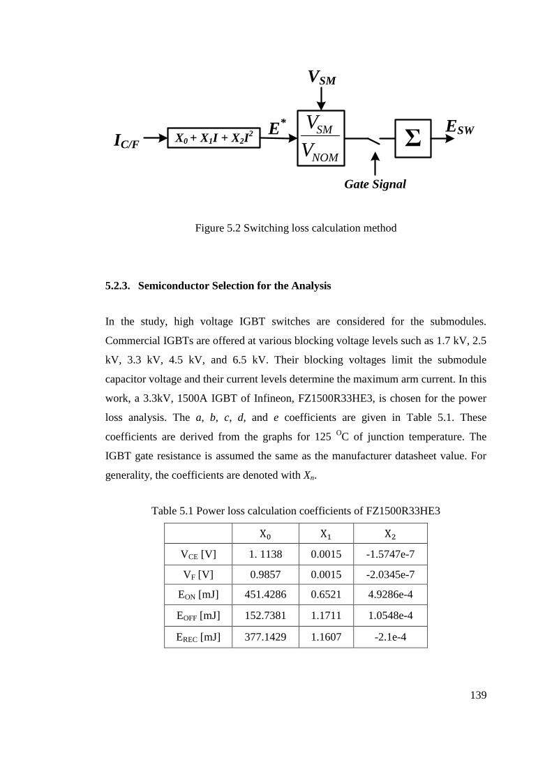
139
ESW
Gate Signal
VSM
X0 + X1I + X2I2
IC/F
E*
NOM
SM
V
VΣ
Figure 5.2 Switching loss calculation method
5.2.3. Semiconductor Selection for the Analysis
In the study, high voltage IGBT switches are considered for the submodules.
Commercial IGBTs are offered at various blocking voltage levels such as 1.7 kV, 2.5
kV, 3.3 kV, 4.5 kV, and 6.5 kV. Their blocking voltages limit the submodule
capacitor voltage and their current levels determine the maximum arm current. In this
work, a 3.3kV, 1500A IGBT of Infineon, FZ1500R33HE3, is chosen for the power
loss analysis. The a, b, c, d, and e coefficients are given in Table 5.1. These
coefficients are derived from the graphs for 125 OC of junction temperature. The
IGBT gate resistance is assumed the same as the manufacturer datasheet value. For
generality, the coefficients are denoted with Xn.
Table 5.1 Power loss calculation coefficients of FZ1500R33HE3
VCE [V] 1. 1138 0.0015 -1.5747e-7
VF [V] 0.9857 0.0015 -2.0345e-7
EON [mJ] 451.4286 0.6521 4.9286e-4
EOFF [mJ] 152.7381 1.1711 1.0548e-4
EREC [mJ] 377.1429 1.1607 -2.1e-4
140
5.3. Case Study
The system under investigation is a 10-MVA MMC tied to a 6-kV medium-voltage
grid and its detailed parameters are shown in Table 4.1. Zero sequence signal of
space vector modulation is injected to output current control signal, Vo_ctrl, to
increase output voltage generation capability.
Throughout the analysis, four different power factor operation condition of the MMC
takes place. Full active power consumption and generation may represent the
converters at the two ends of HVDC system whereas full reactive power processing
illustrates a grid-connected MMC functioning as STATCOM with full inductive or
capacitive loading. For each power factor case, PWM methods with and without
circulating current control are compared in terms of total semiconductor power loss.
Each case has three power loss values calculated with three different sorting
methods. That is, the most useful sorting method in terms of efficiency is sought.
Afterwards, power loss distribution within a submodule is investigated for each
power factor. The loss distribution is also calculated with three sorting applications.
Lastly, the PWM carrier frequency dependency is studied to visualize the power loss
reduction possibility with the utilization of the suitable methods studied in this work.
5.3.1. Total System Losses
At first, power loss dependence on the stored energy is investigated. It is observed
that energy level, i.e. submodule capacitance, influences the losses when circulating
current control is not employed. The simulation is conducted for 24-, 36-, and 48-
kJ/MVA (equivalent to 4-, 6-, and 8-mF submodule capacitances respectively) stored
energy levels. As the energy level increases, power losses accordingly drop off as
shown in Figure 5.3 to Figure 5.6 when circulating current is not employed. The
reason is that circulating current and its losses are naturally decreasing at high stored-
energy levels. On the other hand, circulating current control directly changes the
power loss of MMC. It also improves capacitor voltage ripple and output voltage
141
harmonic distortion. The findings show that circulating current control breaks the
dependence of power loss on stored energy levels as shown in Figure 5.3 to Figure
5.6. Apparently, power loss both decreases and becomes nearly constant over
different submodule capacitances. This is an important result that circulating current
control may lead to the design optimization of less capacitance usage for the same
loss and hence efficiency level.
It can be observed from Figure 5.3 to Figure 5.6 that sorting algorithm choice has
significant impact on total loss. Conventional sorting algorithm results in the largest
power loss while RSF sorting yields the lowest power loss. The improved sorting
algorithm prevents the switching actions when control loop new submodule capacitor
voltage order. This method achieves power loss reduction of 25-35 % of the
conventional method. RSF sorting method further decreases power loss to
approximately 55-65 % of the conventional sorting method in various power factor
and circulating current control conditions studied in this work.
Also, power loss characteristics of phase disposition (PD) and phase-shifted (PS)
PWM methods are observed and it is concluded that PWM methods do not have
major impact as both PWM methods result in similar power losses under the same
operating conditions.

142
(a) PD-PWM with uncontrolled circulating current
(b) PD-PWM with controlled circulating current
(c) PS-PWM with uncontrolled circulating current
(d) PS-PWM with controlled circulating current
Figure 5.3 Total power loss in case of full active power transfer to grid
20 25 30 35 40 45 50
80
100
120
140
160
Energy Level [kJ/MVA]
Po
wer
Lo
ss [
kW
]
Basic Sorting
Improved Sorting
RSF Sorting
20 25 30 35 40 45 50
80
100
120
140
160
Energy Level [kJ/MVA]
Po
wer
Lo
ss [
kW
]
Basic Sorting
Improved Sorting
RSF Sorting
20 25 30 35 40 45 50
80
100
120
140
160
Energy Level [kJ/MVA]
Po
wer
Lo
ss [
kW
]
Basic Sorting
Improved Sorting
RSF Sorting
20 25 30 35 40 45 50
80
100
120
140
160
Energy Level [kJ/MVA]
Po
wer
Lo
ss [
kW
]
Basic Sorting
Improved Sorting
RSF Sorting
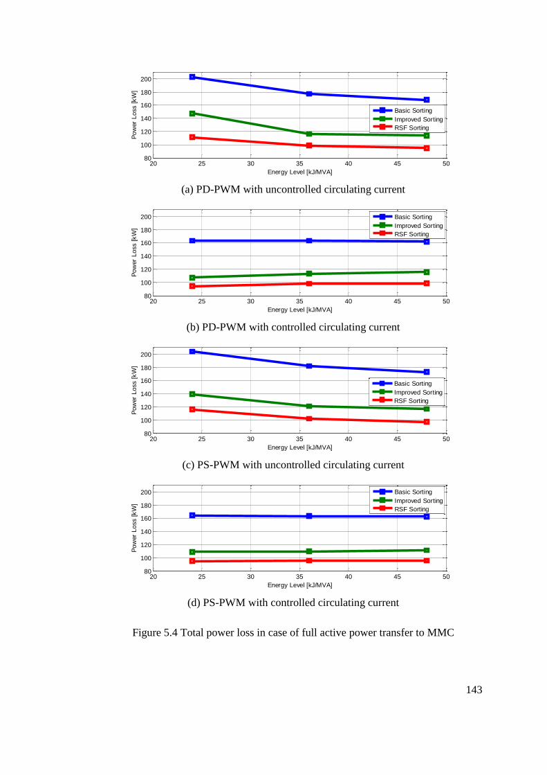
143
(a) PD-PWM with uncontrolled circulating current
(b) PD-PWM with controlled circulating current
(c) PS-PWM with uncontrolled circulating current
(d) PS-PWM with controlled circulating current
Figure 5.4 Total power loss in case of full active power transfer to MMC
20 25 30 35 40 45 5080
100
120
140
160
180
200
Energy Level [kJ/MVA]
Po
wer
Lo
ss [
kW
]
Basic Sorting
Improved Sorting
RSF Sorting
20 25 30 35 40 45 5080
100
120
140
160
180
200
Energy Level [kJ/MVA]
Po
wer
Lo
ss [
kW
]
Basic Sorting
Improved Sorting
RSF Sorting
20 25 30 35 40 45 5080
100
120
140
160
180
200
Energy Level [kJ/MVA]
Po
wer
Lo
ss [
kW
]
Basic Sorting
Improved Sorting
RSF Sorting
20 25 30 35 40 45 5080
100
120
140
160
180
200
Energy Level [kJ/MVA]
Po
wer
Lo
ss [
kW
]
Basic Sorting
Improved Sorting
RSF Sorting
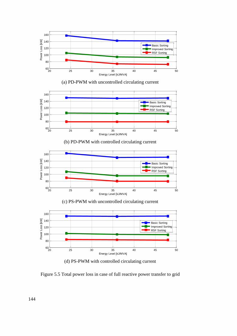
144
(a) PD-PWM with uncontrolled circulating current
(b) PD-PWM with controlled circulating current
(c) PS-PWM with uncontrolled circulating current
(d) PS-PWM with controlled circulating current
Figure 5.5 Total power loss in case of full reactive power transfer to grid
20 25 30 35 40 45 5060
80
100
120
140
160
Energy Level [kJ/MVA]
Po
wer
Lo
ss [
kW
]
Basic Sorting
Improved Sorting
RSF Sorting
20 25 30 35 40 45 5060
80
100
120
140
160
Energy Level [kJ/MVA]
Po
wer
Lo
ss [
kW
]
Basic Sorting
Improved Sorting
RSF Sorting
20 25 30 35 40 45 5060
80
100
120
140
160
Energy Level [kJ/MVA]
Po
wer
Lo
ss [
kW
]
Basic Sorting
Improved Sorting
RSF Sorting
20 25 30 35 40 45 5060
80
100
120
140
160
Energy Level [kJ/MVA]
Po
wer
Lo
ss [
kW
]
Basic Sorting
Improved Sorting
RSF Sorting

145
(a) PD-PWM with uncontrolled circulating current
(b) PD-PWM with controlled circulating current
(c) PS-PWM with uncontrolled circulating current
(d) PS-PWM with controlled circulating current
Figure 5.6 Total power loss in case of full reactive power transfer to MMC
20 25 30 35 40 45 5060
80
100
120
140
160
Energy Level [kJ/MVA]
Po
wer
Lo
ss [
kW
]
Basic Sorting
Improved Sorting
RSF Sorting
20 25 30 35 40 45 5060
80
100
120
140
160
Energy Level [kJ/MVA]
Po
wer
Lo
ss [
kW
]
Basic Sorting
Improved Sorting
RSF Sorting
20 25 30 35 40 45 5060
80
100
120
140
160
Energy Level [kJ/MVA]
Po
wer
Lo
ss [
kW
]
Basic Sorting
Improved Sorting
RSF Sorting
20 25 30 35 40 45 5060
80
100
120
140
160
Energy Level [kJ/MVA]
Po
wer
Lo
ss [
kW
]
Basic Sorting
Improved Sorting
RSF Sorting
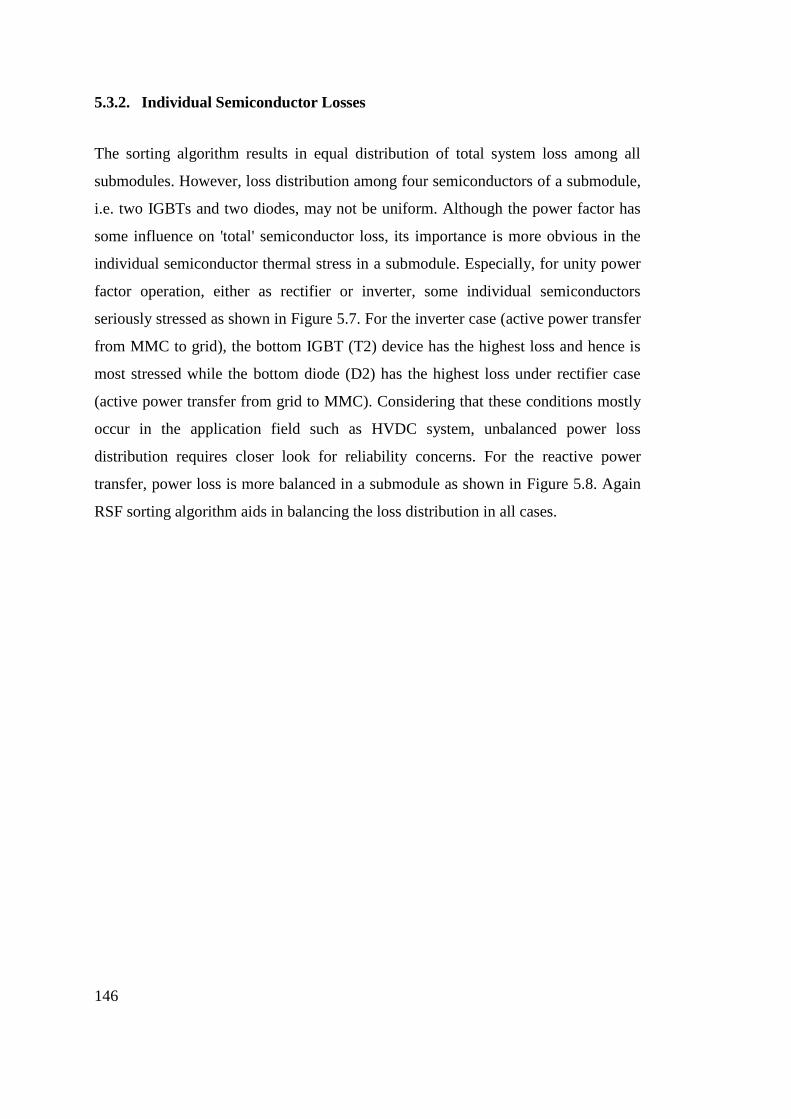
146
5.3.2. Individual Semiconductor Losses
The sorting algorithm results in equal distribution of total system loss among all
submodules. However, loss distribution among four semiconductors of a submodule,
i.e. two IGBTs and two diodes, may not be uniform. Although the power factor has
some influence on 'total' semiconductor loss, its importance is more obvious in the
individual semiconductor thermal stress in a submodule. Especially, for unity power
factor operation, either as rectifier or inverter, some individual semiconductors
seriously stressed as shown in Figure 5.7. For the inverter case (active power transfer
from MMC to grid), the bottom IGBT (T2) device has the highest loss and hence is
most stressed while the bottom diode (D2) has the highest loss under rectifier case
(active power transfer from grid to MMC). Considering that these conditions mostly
occur in the application field such as HVDC system, unbalanced power loss
distribution requires closer look for reliability concerns. For the reactive power
transfer, power loss is more balanced in a submodule as shown in Figure 5.8. Again
RSF sorting algorithm aids in balancing the loss distribution in all cases.
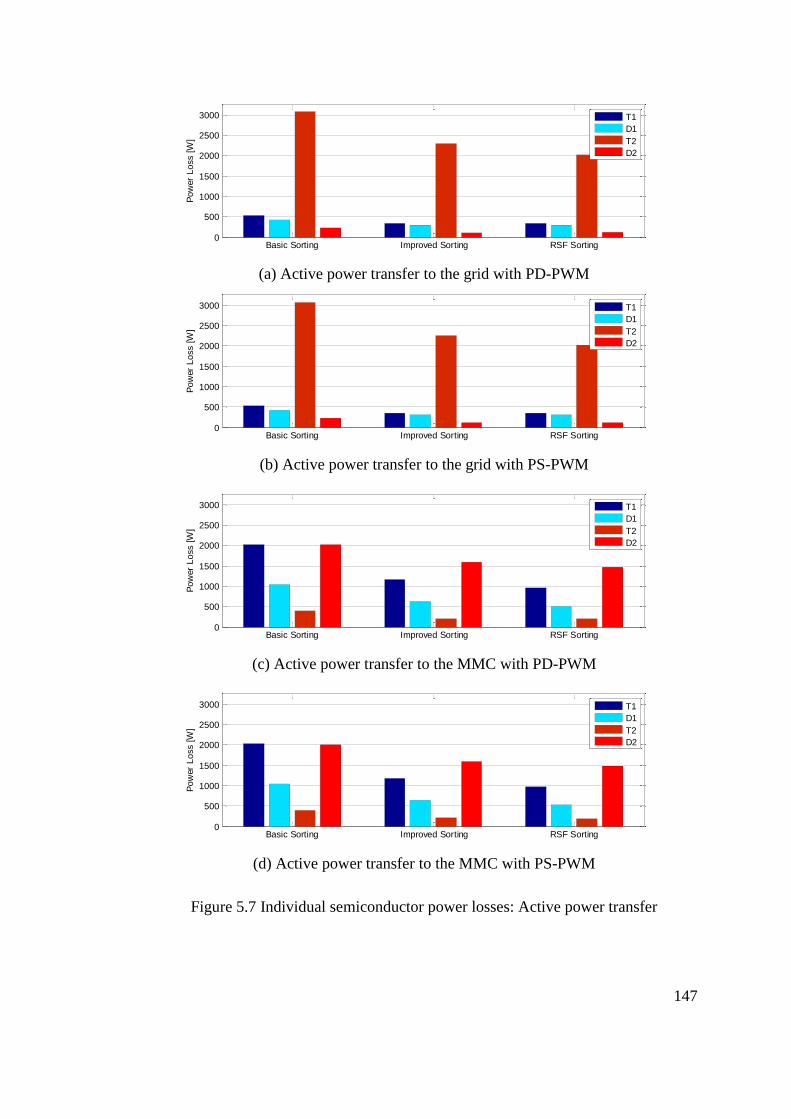
147
(a) Active power transfer to the grid with PD-PWM
(b) Active power transfer to the grid with PS-PWM
(c) Active power transfer to the MMC with PD-PWM
(d) Active power transfer to the MMC with PS-PWM
Figure 5.7 Individual semiconductor power losses: Active power transfer
Basic Sorting Improved Sorting RSF Sorting0
500
1000
1500
2000
2500
3000
Po
wer
Lo
ss [
W]
T1
D1
T2
D2
Basic Sorting Improved Sorting RSF Sorting0
500
1000
1500
2000
2500
3000
Po
wer
Lo
ss [
W]
T1
D1
T2
D2
Basic Sorting Improved Sorting RSF Sorting0
500
1000
1500
2000
2500
3000
Po
wer
Lo
ss [
W]
T1
D1
T2
D2
Basic Sorting Improved Sorting RSF Sorting0
500
1000
1500
2000
2500
3000
Po
wer
Lo
ss [
W]
T1
D1
T2
D2
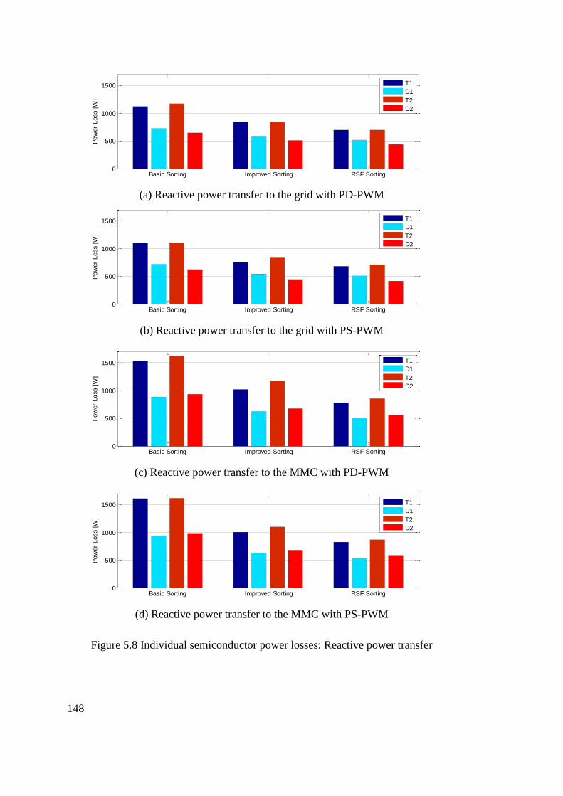
148
(a) Reactive power transfer to the grid with PD-PWM
(b) Reactive power transfer to the grid with PS-PWM
(c) Reactive power transfer to the MMC with PD-PWM
(d) Reactive power transfer to the MMC with PS-PWM
Figure 5.8 Individual semiconductor power losses: Reactive power transfer
Basic Sorting Improved Sorting RSF Sorting0
500
1000
1500
Po
wer
Lo
ss [
W]
T1
D1
T2
D2
Basic Sorting Improved Sorting RSF Sorting0
500
1000
1500
Po
wer
Lo
ss [
W]
T1
D1
T2
D2
Basic Sorting Improved Sorting RSF Sorting0
500
1000
1500
Po
wer
Lo
ss [
W]
T1
D1
T2
D2
Basic Sorting Improved Sorting RSF Sorting0
500
1000
1500
Po
wer
Lo
ss [
W]
T1
D1
T2
D2
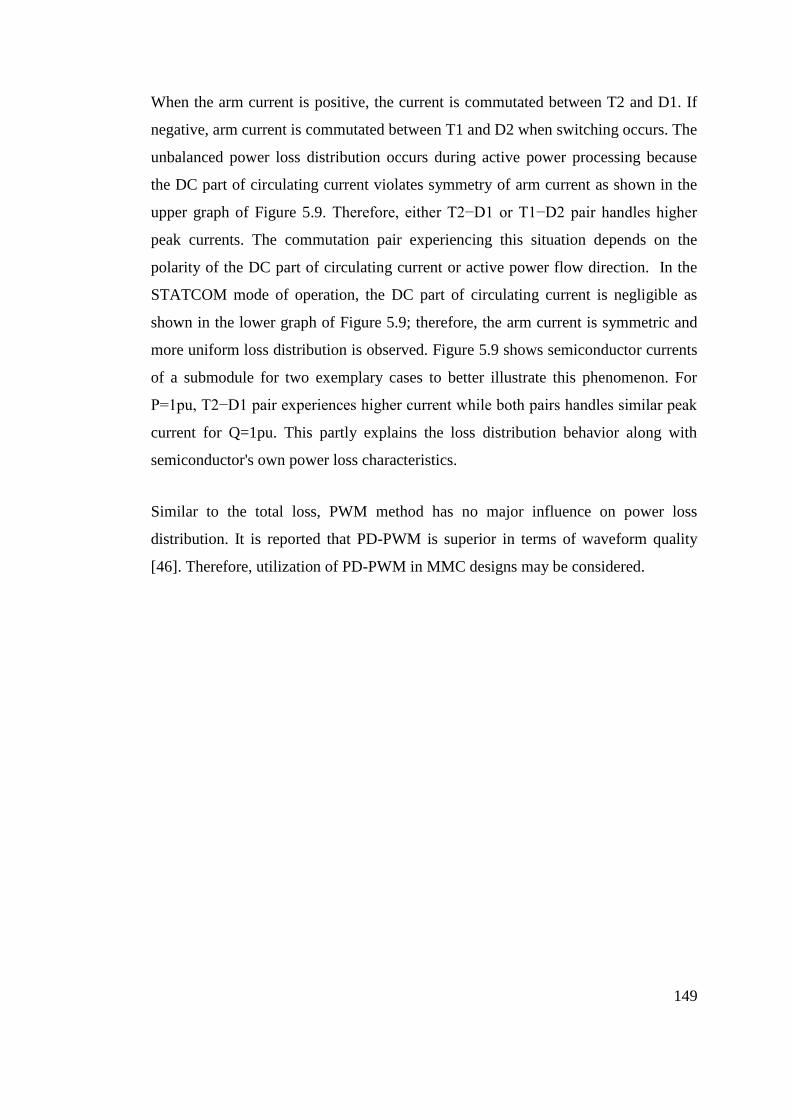
149
When the arm current is positive, the current is commutated between T2 and D1. If
negative, arm current is commutated between T1 and D2 when switching occurs. The
unbalanced power loss distribution occurs during active power processing because
the DC part of circulating current violates symmetry of arm current as shown in the
upper graph of Figure 5.9. Therefore, either T2−D1 or T1−D2 pair handles higher
peak currents. The commutation pair experiencing this situation depends on the
polarity of the DC part of circulating current or active power flow direction. In the
STATCOM mode of operation, the DC part of circulating current is negligible as
shown in the lower graph of Figure 5.9; therefore, the arm current is symmetric and
more uniform loss distribution is observed. Figure 5.9 shows semiconductor currents
of a submodule for two exemplary cases to better illustrate this phenomenon. For
P=1pu, T2−D1 pair experiences higher current while both pairs handles similar peak
current for Q=1pu. This partly explains the loss distribution behavior along with
semiconductor's own power loss characteristics.
Similar to the total loss, PWM method has no major influence on power loss
distribution. It is reported that PD-PWM is superior in terms of waveform quality
[46]. Therefore, utilization of PD-PWM in MMC designs may be considered.
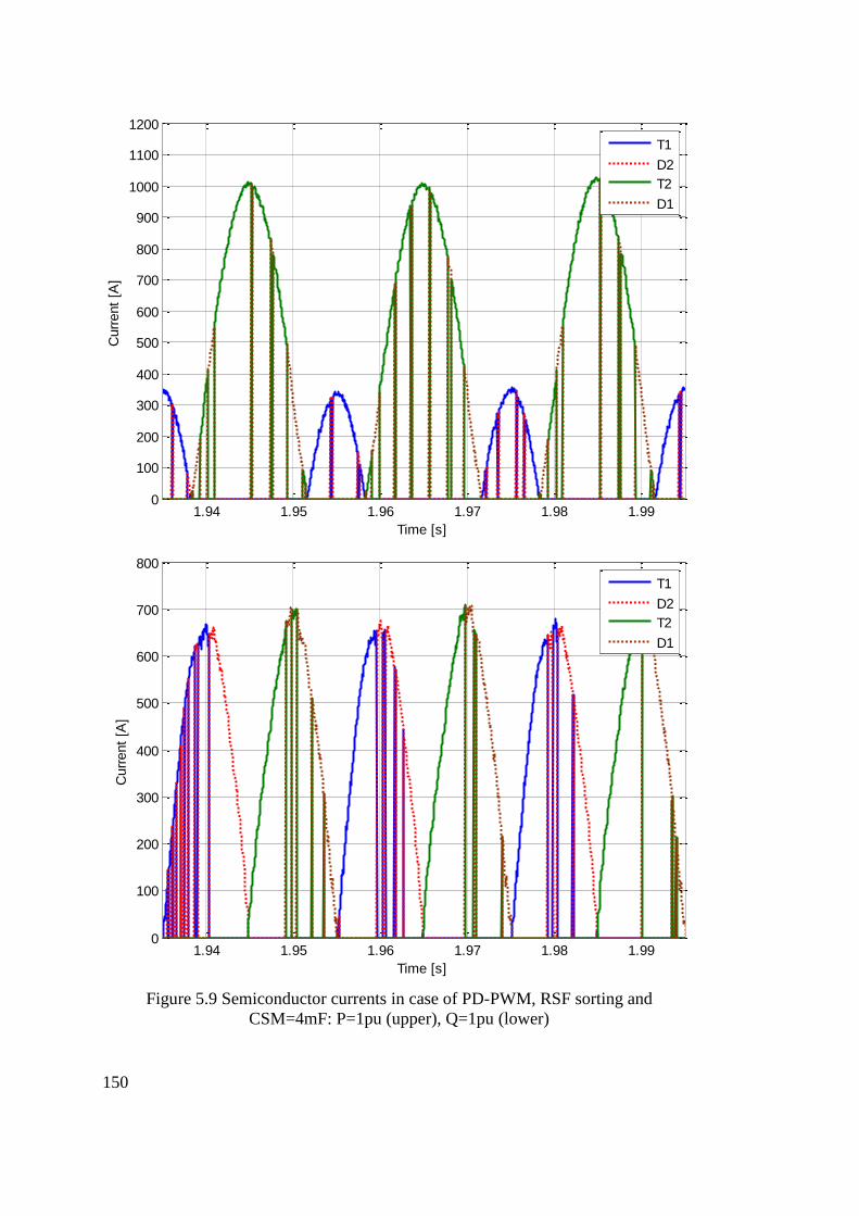
150
Figure 5.9 Semiconductor currents in case of PD-PWM, RSF sorting and
CSM=4mF: P=1pu (upper), Q=1pu (lower)
1.94 1.95 1.96 1.97 1.98 1.990
100
200
300
400
500
600
700
800
900
1000
1100
1200
Time [s]
Curr
ent
[A]
T1
D2
T2
D1
1.94 1.95 1.96 1.97 1.98 1.990
100
200
300
400
500
600
700
800
Time [s]
Curr
ent
[A]
T1
D2
T2
D1

151
5.3.3. PWM Carrier Frequency
In this part, the effect of PWM carrier frequency on power loss is visualized. In
Figure 5.10, the three sorting methods and circulating current control utilization are
compared for the frequency modulation ratio Mf = 15, 45, and 75 cases with PD-
PWM. The solid lines represent the condition with circulating current control while
dashed lines lack this controller.
Figure 5.10 Power loss frequency relation: PD-PWM and CSM=4mF, P=1pu
With the usage of improved or RSF sorting and circulating current control, power
loss can be reduced significantly as the PWM carrier frequency increases. At Mf=75,
the power loss of RSF sorting with circulating current control case is approximately
half of the sorting case without circulating current control. This shows that proper
10 20 30 40 50 60 70 800
25
50
75
100
125
150
175
200
225
250
Frequency Modulation Ratio [Mf]
Pow
er
Loss [
kW
]
Sorting
Improved Sorting
RSF Sorting
Sorting with CCC
Imp. Sort. with CCC
RSF Sort. with CCC
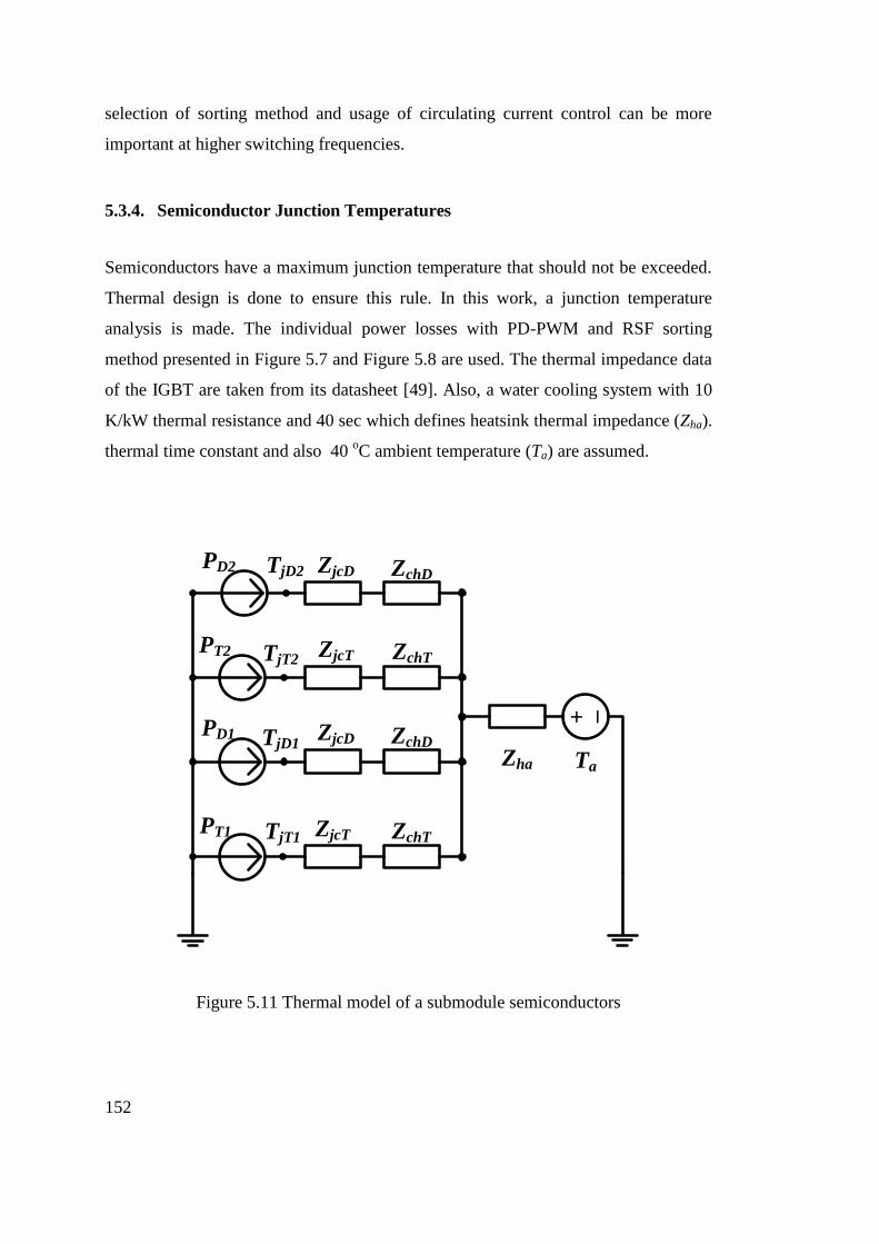
152
selection of sorting method and usage of circulating current control can be more
important at higher switching frequencies.
5.3.4. Semiconductor Junction Temperatures
Semiconductors have a maximum junction temperature that should not be exceeded.
Thermal design is done to ensure this rule. In this work, a junction temperature
analysis is made. The individual power losses with PD-PWM and RSF sorting
method presented in Figure 5.7 and Figure 5.8 are used. The thermal impedance data
of the IGBT are taken from its datasheet [49]. Also, a water cooling system with 10
K/kW thermal resistance and 40 sec which defines heatsink thermal impedance (Zha).
thermal time constant and also 40 oC ambient temperature (Ta) are assumed.
ZchTPT1
PD1
ZjcT
ZchDZjcD
Zha
ZjcD ZchD
ZjcT ZchT
TjT1
_+PD2
PT2
TjD1
TjT2
TjD2
Ta
Figure 5.11 Thermal model of a submodule semiconductors
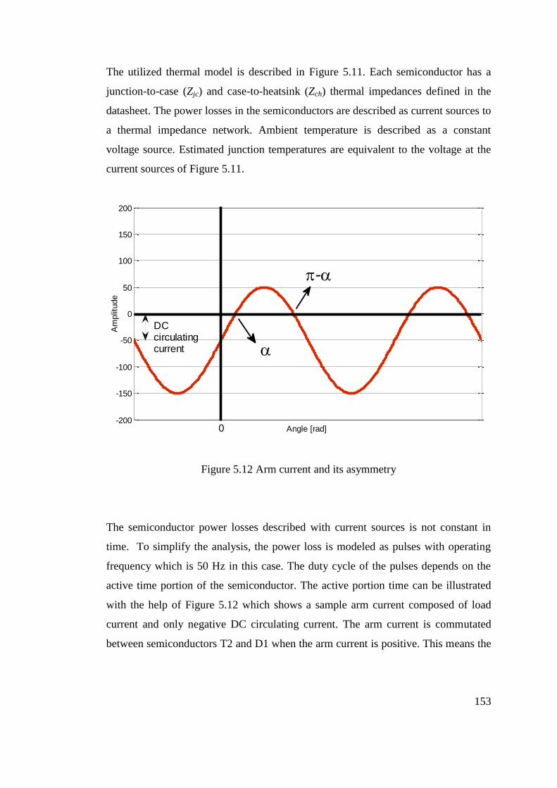
153
The utilized thermal model is described in Figure 5.11. Each semiconductor has a
junction-to-case (Zjc) and case-to-heatsink (Zch) thermal impedances defined in the
datasheet. The power losses in the semiconductors are described as current sources to
a thermal impedance network. Ambient temperature is described as a constant
voltage source. Estimated junction temperatures are equivalent to the voltage at the
current sources of Figure 5.11.
Figure 5.12 Arm current and its asymmetry
The semiconductor power losses described with current sources is not constant in
time. To simplify the analysis, the power loss is modeled as pulses with operating
frequency which is 50 Hz in this case. The duty cycle of the pulses depends on the
active time portion of the semiconductor. The active portion time can be illustrated
with the help of Figure 5.12 which shows a sample arm current composed of load
current and only negative DC circulating current. The arm current is commutated
between semiconductors T2 and D1 when the arm current is positive. This means the
-200
-150
-100
-50
0
50
100
150
200
Angle [rad]
Am
plit
ude
-
DCcirculatingcurrent
0

154
active time portion for T2 and D1 is [α, π-α] and their duty cycle is (π-2α)/(2π). The
angle α is found independently for each operating point. The amplitude of the pulses
is determined to keep lost energy constant. That means the amplitudes of the pulses
become (2πP)/(π-2α) where P is the lost average power in the semiconductor. For the
T1 and D2 pair, duty cycle of the pulse becomes (π+2α)/(2π) because they are active
in the angles [π-α, 2π+α]. Also, the amplitudes of the pulses are (2πP)/(π+2α). Notice
that duty cycles and amplitude of pulses are calculated for the case of Figure 5.12.
When the amplitude of direction of the DC circulating current changes, the duty
cycles and pulse amplitudes should be calculated accordingly.
The steady-state junction temperature for full active power generation to grid is
given in Figure 5.13a. The highest temperature belongs to T2 which has also the
highest power loss. The case of the full active power flow to MMC is given in Figure
5.13b where D2 seems to have the highest temperature. The active power processing
cases show a unique characteristic in their junction temperature as predicted in
Section 5.3.2. In both cases, one semiconductor temperature are comparatively
higher than the remaining. Therefore, these semiconductors are the limiting factor in
thermal design.
The junction temperatures for the cases of reactive power exchange between MMC
and grid are presented in Figure 5.14. They all follow nearly the same temperature.
As discussed in Section 5.3.2, the reactive power cases have relatively balanced
power losses among the semiconductors in the submodule. This fact is simply
reflected to junction temperature behavior.
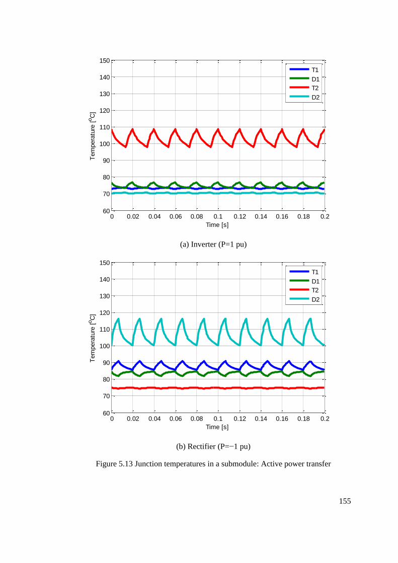
155
(a) Inverter (P=1 pu)
(b) Rectifier (P=−1 pu)
Figure 5.13 Junction temperatures in a submodule: Active power transfer
0 0.02 0.04 0.06 0.08 0.1 0.12 0.14 0.16 0.18 0.260
70
80
90
100
110
120
130
140
150
Time [s]
Tem
pera
ture
[oC
]
T1
D1
T2
D2
0 0.02 0.04 0.06 0.08 0.1 0.12 0.14 0.16 0.18 0.260
70
80
90
100
110
120
130
140
150
Time [s]
Tem
pera
ture
[oC
]
T1
D1
T2
D2
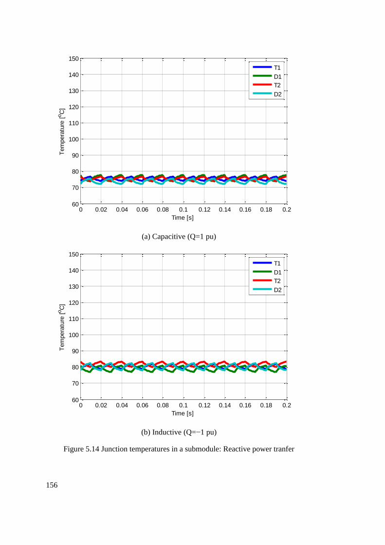
156
(a) Capacitive (Q=1 pu)
(b) Inductive (Q=−1 pu)
Figure 5.14 Junction temperatures in a submodule: Reactive power tranfer
0 0.02 0.04 0.06 0.08 0.1 0.12 0.14 0.16 0.18 0.260
70
80
90
100
110
120
130
140
150
Time [s]
Tem
pera
ture
[oC
]
T1
D1
T2
D2
0 0.02 0.04 0.06 0.08 0.1 0.12 0.14 0.16 0.18 0.260
70
80
90
100
110
120
130
140
150
Time [s]
Tem
pera
ture
[oC
]
T1
D1
T2
D2
157
5.4. Conclusion
This chapter investigated the total and distributed power semiconductor losses in a
submodule of the MMC converter. The influence of the submodule capacitor size
(the stored energy value), the circulating current control utilization, the PWM
method, the switching algorithm and finally the frequency modulation ratio on the
total and distributed power semiconductor losses have been all investigated in detail.
It has been shown that the circulating current control method is more effective than
increasing the stored energy (the submodule capacitance value) for reducing the
power semiconductor stresses and losses. Thus, the importance of using such a
method as an active control method, rather than suppression of losses by large
passive components is more favorable.
It has also been shown that the switching algorithm strongly influences the losses and
advanced sorting methods provide significant loss performance enhancements. RSF
sorting provides significant loss reduction compared to the basic sorting method.
Elevated PWM carrier frequency further increases this importance.
Additionally, it has been demonstrated that PD- and PS-PWM techniques exhibit no
major performance difference in terms of the total power loss and its distribution
among semiconductors. Also, for unity power factor operation, power loss
distribution in a submodule is not uniform. This is attributed to DC component of
circulating current. Considering that MMC systems are likely to operate around unity
power factor either rectifier or inverter sides of HVDC links, this issue requires
special attention.
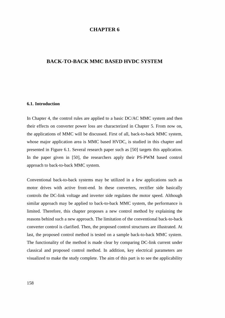
158
CHAPTER 6
6. BACK-TO-BASED MMC BASED HVDC SYSTEM
BACK-TO-BACK MMC BASED HVDC SYSTEM
6.1. Introduction
In Chapter 4, the control rules are applied to a basic DC/AC MMC system and then
their effects on converter power loss are characterized in Chapter 5. From now on,
the applications of MMC will be discussed. First of all, back-to-back MMC system,
whose major application area is MMC based HVDC, is studied in this chapter and
presented in Figure 6.1. Several research paper such as [50] targets this application.
In the paper given in [50], the researchers apply their PS-PWM based control
approach to back-to-back MMC system.
Conventional back-to-back systems may be utilized in a few applications such as
motor drives with active front-end. In these converters, rectifier side basically
controls the DC-link voltage and inverter side regulates the motor speed. Although
similar approach may be applied to back-to-back MMC system, the performance is
limited. Therefore, this chapter proposes a new control method by explaining the
reasons behind such a new approach. The limitation of the conventional back-to-back
converter control is clarified. Then, the proposed control structures are illustrated. At
last, the proposed control method is tested on a sample back-to-back MMC system.
The functionality of the method is made clear by comparing DC-link current under
classical and proposed control method. In addition, key electrical parameters are
visualized to make the study complete. The aim of this part is to see the applicability
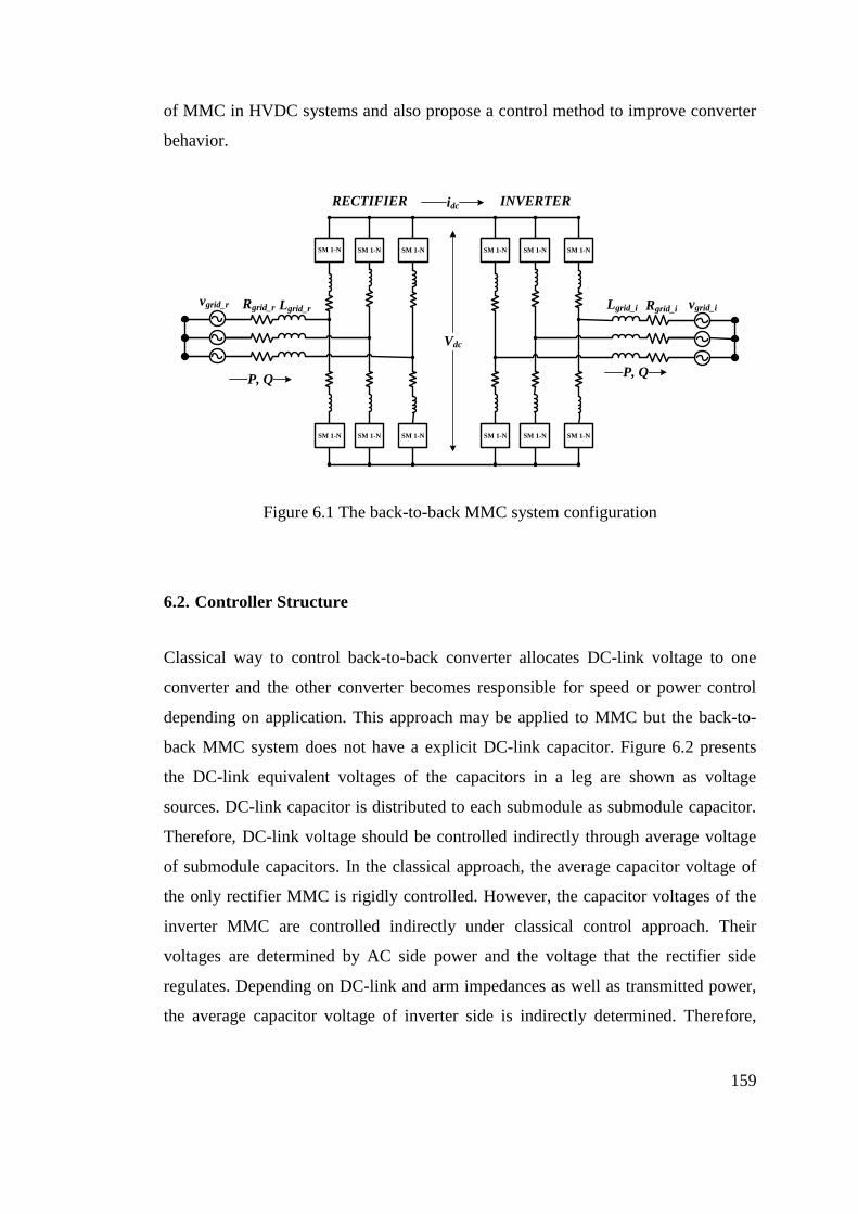
159
of MMC in HVDC systems and also propose a control method to improve converter
behavior.
Rgrid_i vgrid_iLgrid_i
SM 1-N
SM 1-N
SM 1-N
SM 1-N
SM 1-N
SM 1-N
SM 1-N
SM 1-N
SM 1-N
SM 1-N
SM 1-N
SM 1-N
Rgrid_rvgrid_r Lgrid_r
Vdc
RECTIFIER INVERTERidc
P, QP, Q
Figure 6.1 The back-to-back MMC system configuration
6.2. Controller Structure
Classical way to control back-to-back converter allocates DC-link voltage to one
converter and the other converter becomes responsible for speed or power control
depending on application. This approach may be applied to MMC but the back-to-
back MMC system does not have a explicit DC-link capacitor. Figure 6.2 presents
the DC-link equivalent voltages of the capacitors in a leg are shown as voltage
sources. DC-link capacitor is distributed to each submodule as submodule capacitor.
Therefore, DC-link voltage should be controlled indirectly through average voltage
of submodule capacitors. In the classical approach, the average capacitor voltage of
the only rectifier MMC is rigidly controlled. However, the capacitor voltages of the
inverter MMC are controlled indirectly under classical control approach. Their
voltages are determined by AC side power and the voltage that the rectifier side
regulates. Depending on DC-link and arm impedances as well as transmitted power,
the average capacitor voltage of inverter side is indirectly determined. Therefore,
160
under dynamic conditions, settling of the capacitors in the inverter MMC may be
floppy.
vΣ
BvΣ
A vΣ
C
2Larm
2Rarm
vΣ
BvΣ
C vΣ
A
2Rarm2Rarm
2Larm2Larm
2Rarm2Rarm2Rarm
2Larm2Larm2Larm
Vdc
idc INVERTERRECTIFIER
Figure 6.2 DC-link equivalent circuit of back-to-back MMC system
In addition, power transfer between rectifier and inverter sides depends on the
equivalent DC-link voltage difference between two MMCs. Therefore, the DC-link
current and hence transmitted power may also be affected by the loose voltage
dynamics of the inverter side. This can be also be understood in the simplified DC-
link equivalent circuit of back-to-back MMC system in Figure 6.3. The equivalent
DC-link voltages are modeled in Figure 6.3 as Vrec and Vinv for rectifier and inverter
sides, respectively. Any loose variation in these voltages will affect DC-link current
and power transfer, and then AC-side variables. That means, both should be firmly
regulated.
Therefore, this thesis proposes an improvement to this control. Instead of using
inverter side to control the its own capacitor voltages, both converters should
'independently' regulate their average capacitor voltages. In this way, the capacitors
at both sides are rigidly controlled. However, if the average capacitor voltages of

161
both rectifier and inverter sides are regulated to same value, Vrec and Vinv become
also same. That means power transfer ideally cannot occur because the power-
carrying DC-link current flows under voltage difference between two sides.
Therefore, DC-link equivalent voltage of the inverter MMC, Vinv, should be actively
controlled to enable power flow from rectifier to inverter side or vice versa.
Vrec
Req
Leq
Vdc
idc INVERTERRECTIFIER
Leq
Req
Vinv
Figure 6.3 Simplified DC-link equivalent circuit of back-to-back MMC system
That means the proposed control has two steps. First one is to control average
voltages of all capacitors at "both" rectifier and inverter side independently. Second
step is to control DC-link equivalent voltage of "only" one side, possibly inverter
side, through control of DC part of circulating current. In this way, irrespective of
loading level and voltage drop between converters, all capacitor voltage are regulated
to same voltage and oscillatory dynamics are eliminated.
Inverter side will also control DC part of circulating current in the proposed control
approach. In this way, all components of circulating current are controlled because
previously only eliminating its second-harmonic component was considered. DC part
of the circulating current is the current at DC-link as power transfer mean. The
controller adjusts the DC-link equivalent voltage of the inverter side in order to
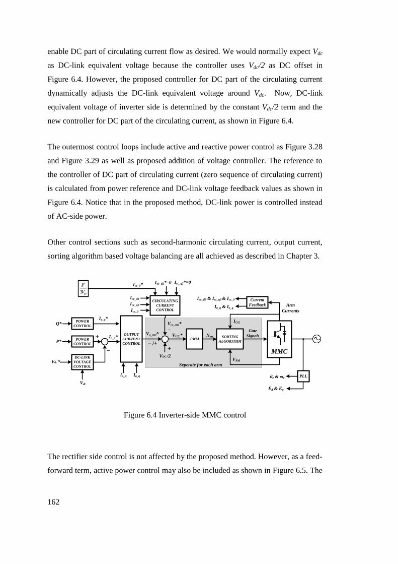
162
enable DC part of circulating current flow as desired. We would normally expect Vdc
as DC-link equivalent voltage because the controller uses Vdc/2 as DC offset in
Figure 6.4. However, the proposed controller for DC part of the circulating current
dynamically adjusts the DC-link equivalent voltage around Vdc. Now, DC-link
equivalent voltage of inverter side is determined by the constant Vdc/2 term and the
new controller for DC part of the circulating current, as shown in Figure 6.4.
The outermost control loops include active and reactive power control as Figure 3.28
and Figure 3.29 as well as proposed addition of voltage controller. The reference to
the controller of DC part of circulating current (zero sequence of circulating current)
is calculated from power reference and DC-link voltage feedback values as shown in
Figure 6.4. Notice that in the proposed method, DC-link power is controlled instead
of AC-side power.
Other control sections such as second-harmonic circulating current, output current,
sorting algorithm based voltage balancing are all achieved as described in Chapter 3.
– /+
VDC /2
Vo_ctrl*
Vcc_ctrl*
+
PWM
Gate
SignalsSORTING
ALGORITHM
NonVU/L*OUTPUT
CURRENT
CONTROL
Q*
CIRCULATING
CURRENT
CONTROL
–
Icc_q2*=0
Seperate for each arm
POWER
CONTROL
Icc_d2*=0
Io_q*
MMC
PLLθe & ωe
Ed & Eq
VSM
Io_q Io_q
IU/L
Current
FeedbackIo_q & Io_qArm
Currents
Icc_d2
Icc_q2
Icc_d2 & Icc_q2 & Icc_0
DC-LINK
VOLTAGE
CONTROL
Vdc *
Io_d*
Vdc
P*POWER
CONTROL
+
–
dcV
P
3
*
Icc_0
Icc_0*
Figure 6.4 Inverter-side MMC control
The rectifier side control is not affected by the proposed method. However, as a feed-
forward term, active power control may also be included as shown in Figure 6.5. The
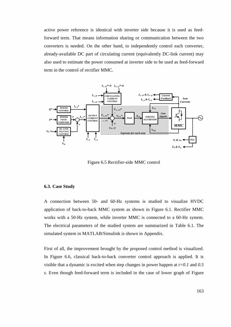
163
active power reference is identical with inverter side because it is used as feed-
forward term. That means information sharing or communication between the two
converters is needed. On the other hand, to independently control each converter,
already-available DC part of circulating current (equivalently DC-link current) may
also used to estimate the power consumed at inverter side to be used as feed-forward
term in the control of rectifier MMC.
– /+
VDC /2
Vo_ctrl*
Vcc_ctrl*
+
PWM
Gate
SignalsSORTING
ALGORITHM
NonVU/L*OUTPUT
CURRENT
CONTROL
Q*
CIRCULATING
CURRENT
CONTROL
–
Icc_q2*=0
Seperate for each arm
POWER
CONTROL
Icc_d2*=0
Io_q*
MMC
PLLθe & ωe
Ed & Eq
VSM
Io_q Io_q
IU/L
Current
FeedbackIo_q & Io_qArm
Currents
Icc_d2
Icc_q2
Icc_d2 & Icc_q2
DC-LINK
VOLTAGE
CONTROL
Vdc *
Io_d*
Vdc
P*POWER
FEED-
FORWARD
+
+
Figure 6.5 Rectifier-side MMC control
6.3. Case Study
A connection between 50- and 60-Hz systems is studied to visualize HVDC
application of back-to-back MMC system as shown in Figure 6.1. Rectifier MMC
works with a 50-Hz system, while inverter MMC is connected to a 60-Hz system.
The electrical parameters of the studied system are summarized in Table 6.1. The
simulated system in MATLAB/Simulink is shown in Appendix.
First of all, the improvement brought by the proposed control method is visualized.
In Figure 6.6, classical back-to-back converter control approach is applied. It is
visible that a dynamic is excited when step changes in power happen at t=0.1 and 0.5
s. Even though feed-forward term is included in the case of lower graph of Figure
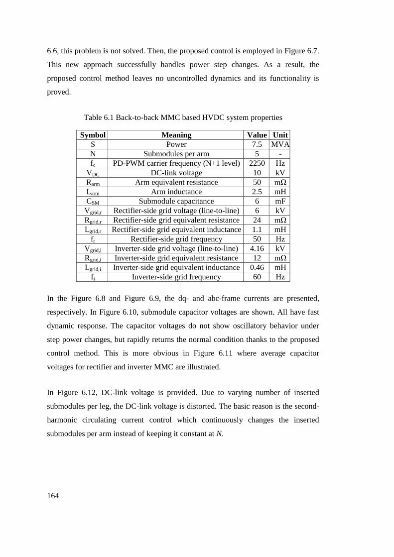
164
6.6, this problem is not solved. Then, the proposed control is employed in Figure 6.7.
This new approach successfully handles power step changes. As a result, the
proposed control method leaves no uncontrolled dynamics and its functionality is
proved.
Table 6.1 Back-to-back MMC based HVDC system properties
Symbol Meaning Value Unit
S Power 7.5 MVA
N Submodules per arm 5 -
fc PD-PWM carrier frequency (N+1 level) 2250 Hz
VDC DC-link voltage 10 kV
Rarm Arm equivalent resistance 50 mΩ
Larm Arm inductance 2.5 mH
CSM Submodule capacitance 6 mF
Vgrid,r Rectifier-side grid voltage (line-to-line) 6 kV
Rgrid,r Rectifier-side grid equivalent resistance 24 mΩ
Lgrid,r Rectifier-side grid equivalent inductance 1.1 mH
fr Rectifier-side grid frequency 50 Hz
Vgrid,i Inverter-side grid voltage (line-to-line) 4.16 kV
Rgrid,i Inverter-side grid equivalent resistance 12 mΩ
Lgrid,i Inverter-side grid equivalent inductance 0.46 mH
fi Inverter-side grid frequency 60 Hz
In the Figure 6.8 and Figure 6.9, the dq- and abc-frame currents are presented,
respectively. In Figure 6.10, submodule capacitor voltages are shown. All have fast
dynamic response. The capacitor voltages do not show oscillatory behavior under
step power changes, but rapidly returns the normal condition thanks to the proposed
control method. This is more obvious in Figure 6.11 where average capacitor
voltages for rectifier and inverter MMC are illustrated.
In Figure 6.12, DC-link voltage is provided. Due to varying number of inserted
submodules per leg, the DC-link voltage is distorted. The basic reason is the second-
harmonic circulating current control which continuously changes the inserted
submodules per arm instead of keeping it constant at N.
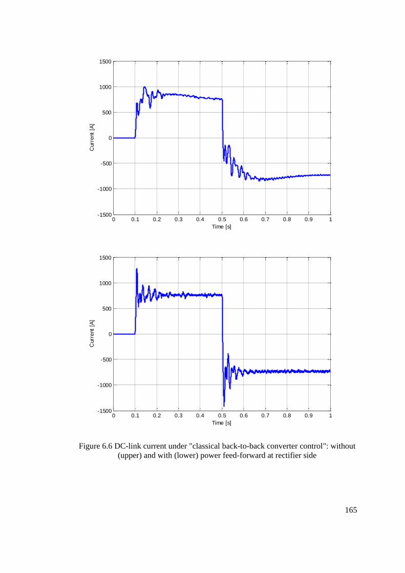
165
Figure 6.6 DC-link current under "classical back-to-back converter control": without
(upper) and with (lower) power feed-forward at rectifier side
0 0.1 0.2 0.3 0.4 0.5 0.6 0.7 0.8 0.9 1-1500
-1000
-500
0
500
1000
1500
Curr
ent
[A]
Time [s]
0 0.1 0.2 0.3 0.4 0.5 0.6 0.7 0.8 0.9 1-1500
-1000
-500
0
500
1000
1500
Curr
ent
[A]
Time [s]
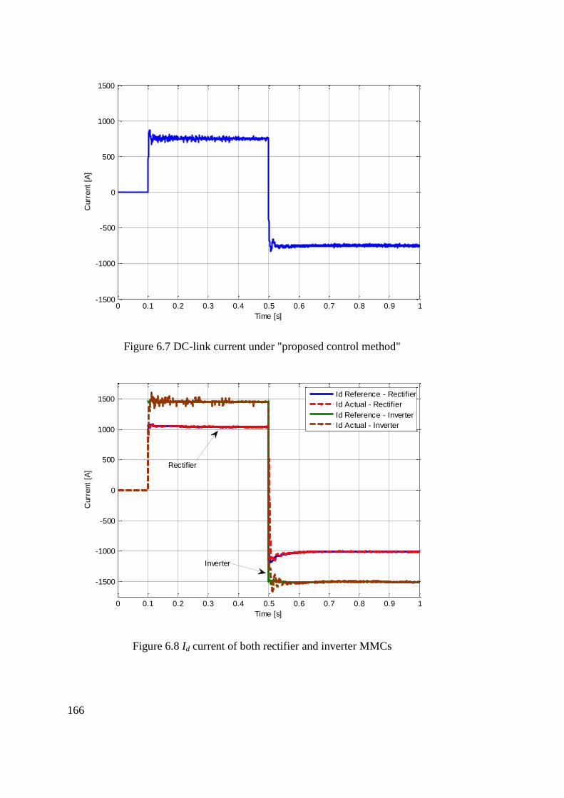
166
Figure 6.7 DC-link current under "proposed control method"
Figure 6.8 Id current of both rectifier and inverter MMCs
0 0.1 0.2 0.3 0.4 0.5 0.6 0.7 0.8 0.9 1-1500
-1000
-500
0
500
1000
1500C
urr
ent
[A]
Time [s]
0 0.1 0.2 0.3 0.4 0.5 0.6 0.7 0.8 0.9 1
-1500
-1000
-500
0
500
1000
1500
Curr
ent
[A]
Time [s]
Id Reference - Rectifier
Id Actual - Rectifier
Id Reference - Inverter
Id Actual - Inverter
Rectifier
Inverter
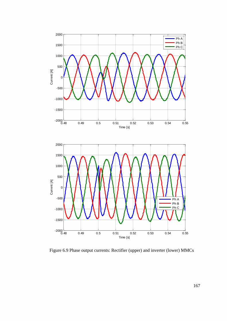
167
Figure 6.9 Phase output currents: Rectifier (upper) and inverter (lower) MMCs
0.48 0.49 0.5 0.51 0.52 0.53 0.54 0.55-2000
-1500
-1000
-500
0
500
1000
1500
2000
Curr
ent
[A]
Time [s]
Ph A
Ph B
Ph C
0.48 0.49 0.5 0.51 0.52 0.53 0.54 0.55-2000
-1500
-1000
-500
0
500
1000
1500
2000
Curr
ent
[A]
Time [s]
Ph A
Ph B
Ph C
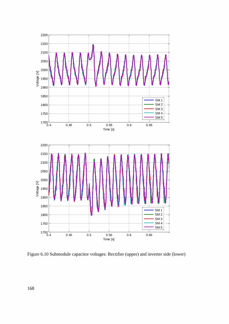
168
Figure 6.10 Submodule capacitor voltages: Rectifier (upper) and inverter side (lower)
0.4 0.45 0.5 0.55 0.6 0.651700
1750
1800
1850
1900
1950
2000
2050
2100
2150
2200V
olt
age
[V
]
Time [s]
SM 1
SM 2
SM 3
SM 4
SM 5
0.4 0.45 0.5 0.55 0.6 0.651700
1750
1800
1850
1900
1950
2000
2050
2100
2150
2200
Volt
age
[V
]
Time [s]
SM 1
SM 2
SM 3
SM 4
SM 5
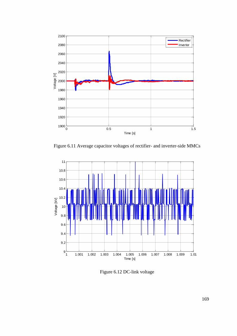
169
Figure 6.11 Average capacitor voltages of rectifier- and inverter-side MMCs
Figure 6.12 DC-link voltage
0 0.5 1 1.51900
1920
1940
1960
1980
2000
2020
2040
2060
2080
2100
Volt
age
[V
]
Time [s]
Rectifier
Inverter
1 1.001 1.002 1.003 1.004 1.005 1.006 1.007 1.008 1.009 1.019
9.2
9.4
9.6
9.8
10
10.2
10.4
10.6
10.8
11
Volt
age
[kV
]
Time [s]
170
6.4. Summary
In this chapter, control of back-to-back MMC system is studied. The aim of this part
is to see the applicability of MMC in HVDC systems and also propose a control
method to improve converter behavior. The limitation of classical back-to-back
converter control when employed in the control of back-to-back connected MMCs is
emphasized. Back-to-back MMC system does not have common DC-link capacitor,
but each converter independently has submodule capacitors in place of the common
DC-link capacitor. Controlling DC-link voltage at rectifier side does not mean rigid
control also at inverter side because the capacitors are separated by the arm and DC-
link impedances. Therefore, DC-link control by rectifier does not provide good
performance in dynamic condition. As a result, this chapter proposes a new control
method targeting this problem. Both converters should regulate the average voltage
of its submodule capacitors. However, this is not enough. DC-part of circulating
current is also regulated by adjusting DC-link equivalent voltage of inverter side.
In short, the proposed control has two parts. First one is to control average voltages
of all capacitors at "both" rectifier and inverter side independently. Second part is to
control DC-link equivalent voltage of "only" one side, possibly inverter side, through
control of DC part of circulating current. In this way, regardless of loading level and
voltage drop between converters, all capacitor voltage are regulated to same voltage
and oscillatory dynamics are eliminated.
At last, the proposed control method is visualized on a sample back-to-back MMC
system. Improvement in the dynamic response is made clear by comparing DC-link
current under classical and proposed control method. In addition, key electrical
parameters are visualized to make the study complete.
DC-link voltage contains high distortion when circulating current control is utilized.
The reason is that circulating current control causes the number of inserted
submodules per arm to vary. Originally, it was N when the circulating current control

171
is not used. But now, it may be N-1, N, or N+1. Since the DC link does not have a
high-value explicit capacitor between the two MMCs, the DC link is not stiff.
Therefore, combining the effects of both inverter and rectifier MMCs, the waveform
of the DC-link voltage is distorted. As a result, DC-link is indirectly regulated
through average voltage of submodule capacitor. Taking average eliminates intrinsic
low-order harmonic voltages in an individual capacitor. Thanks to this control as
well as sorting algorithm based balancing, submodule capacitor voltages do not
diverge under sharp power changes and are kept balanced.
172
CHAPTER 7
7. MMC BASED MOTOR DRIVE SYSTEM
MMC BASED MOTOR DRIVE SYSTEM
7.1. Introduction
The special case of low-frequency operation of MMC is investigated in this chapter.
The importance of the low-frequency operation comes from medium-voltage motor
drive. Motors may be operated at lower speeds than the rated speed or at least, start-
up of the motors requires low-frequency operation. Therefore, MMC based motor
drives should handle the low-frequency operation. The control approach to solve this
problem is presented in this chapter.
The voltage ripples in the submodule capacitors are proportional to the current
amplitude and the inversely proportional to the submodule capacitance and operating
frequency [17]. Due to the voltage ripples, voltage rating of semiconductors and
submodule capacitor may be violated. Thus, the operation in low frequencies is
challenging.
The first study that proposes a method for the low frequency operation of MMC is
the paper written by Korn, Winkelnkemper, and Steimer in 2010 [22]. Their method
basically forces a circulating current with higher frequency so that the frequency of
voltage ripple is mainly shifted to higher values. In addition to circulating current, a
common mode voltage with the frequency of the forced circulating current is also
used. The injected common mode voltage and the forced circulating current basically
173
do not affect the output current and the machine control. However, since the forced
circulating current occupies a current capacity and similarly the injected common
mode voltage also uses some of the voltage capacity of MMC, the achievable torque
at low frequencies is limited. On the other hand, the proposed control approach at
least enables the usage of MMC in motor drives. As a result, MMC based motor
drives are thought to be suitable for variable torque loads such as fan/blower which
need low torque in low frequencies.
7.2. The Control Method for Low Frequency Operation
In Equations (8.1) and (8.2), the power dynamics inside the upper and lower arm are
presented where vo and io are the output voltage reference and output current of an
arbitrary phase. If the operating frequency is denoted by f, the power relations
include the components with f and 2f frequencies as well as DC component.
However, the low-frequency fluctuation in the arm powers or alternatively the
energy stored in the capacitors is not desired.
(8.1)
(8.2)
As a solution, a common mode voltage, vcm, is injected into the output voltage
reference, vo. And also a circulating current is consciously forced. In the constant
frequency applications such as grid-tied MMCs, the second-harmonic circulating
current is controlled to zero. However, in low frequency operation of MMC, the
common mode voltage and the circulating current provides the degree of freedom.
The new resulting power dynamic of the arms are provided in Equations (8.3) and
(8.4).
174
(8.3)
(8.4)
The Equations (8.3) and (8.4) may be grouped into the common mode and
differential mode parts.
(8.5)
(8.6)
(8.7)
(8.8)
In the common mode power expression in Equation (8.7), the low frequency
oscillation comes from
term. One part of the forced circulating current is used to
cancel out this term. Therefore, common mode part of the circulating current is
expressed as Equation (8.9).
(8.9)
Similarly, low frequency oscillation in the differential mode power expression in
Equation (8.8) can be eliminated by Equation (8.10).
(8.10)
The resultant power equations are written in Equations (8.11) and (8.12).
175
(8.11)
(8.12)
Notice that all low-frequency output terms in Equations (8.11) and (8.12) have one
high frequency term in multiplication. Therefore, the total power or energy
oscillations in the arms are now at the high frequency. This frequency is determined
by the frequency of the common mode voltage, vcm.
The expression for the common mode voltage, vcm, and the circulating current, icc,
[41] are given in Equations (8.13) and (8.14). Notice that the common mode voltage
is common to all phases and is added to each phase reference. On the other hand, the
circulating current reference should be calculated to each phase separately. As an
example, the circulating current reference for phase-A is given in Equation (8.15).
(8.13)
(8.14)
(8.15)
The amplitude, Vcm, and the frequency, fcm, of the chosen common-mode voltage
determines the numerical values of the common-mode voltage that is included in the
arm voltage reference and the reference circulating current that should be followed.
In [41], it is advised that fcm should be more than three times the electrical frequency
that the low-frequency operation mode is utilized. Also, fcm needs to be lower than
the one tenth of the equivalent switching frequency for good controllability. The
amplitude of the common mode voltage is chosen not to enter into over-modulation.
That is, the sum of the voltage coming from the output current controller and the
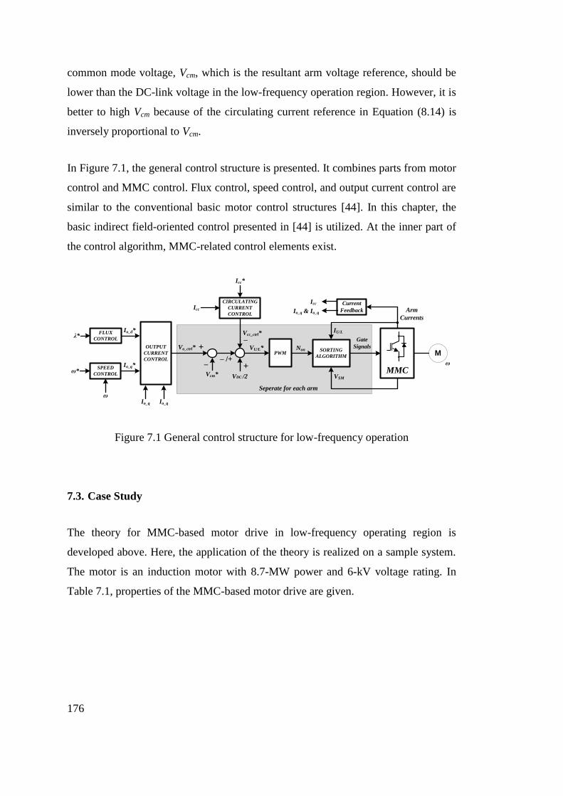
176
common mode voltage, Vcm, which is the resultant arm voltage reference, should be
lower than the DC-link voltage in the low-frequency operation region. However, it is
better to high Vcm because of the circulating current reference in Equation (8.14) is
inversely proportional to Vcm.
In Figure 7.1, the general control structure is presented. It combines parts from motor
control and MMC control. Flux control, speed control, and output current control are
similar to the conventional basic motor control structures [44]. In this chapter, the
basic indirect field-oriented control presented in [44] is utilized. At the inner part of
the control algorithm, MMC-related control elements exist.
– /+
VDC /2Vcm*
Vo_ctrl*
+
PWM
Gate
SignalsSORTING
ALGORITHM
NonVU/L*OUTPUT
CURRENT
CONTROL
λ*
CIRCULATING
CURRENT
CONTROL
–
Icc*
Seperate for each arm
FLUX
CONTROL
ω*Io_q*
Io_d*
–
+
SPEED
CONTROL
Vcc_ctrl*
Io_q Io_q
MMC
M
VSM
Current
FeedbackIo_q & Io_qArm
Currents
Icc
Icc
ω
ω
IU/L
Figure 7.1 General control structure for low-frequency operation
7.3. Case Study
The theory for MMC-based motor drive in low-frequency operating region is
developed above. Here, the application of the theory is realized on a sample system.
The motor is an induction motor with 8.7-MW power and 6-kV voltage rating. In
Table 7.1, properties of the MMC-based motor drive are given.

177
Table 7.1 MMC-based motor drive properties
Symbol Meaning Value Unit
S Converter rated power 10 MVA
N Submodules per arm 5 -
fc PD-PWM carrier frequency (N+1 level) 4500 Hz
Vdc DC-link voltage 10 kVdc
Rarm Arm equivalent resistance 50 mΩ
Larm Arm inductance 2.5 mH
CSM Submodule capacitance 6 mF
Vcm Common-mode voltage 3500 Vpeak
fcm Common-mode frequency 45 Hz
Pmech Motor rated mechanical power 8.7 MW
Vmotor Motor rated voltage (line-to-line) 6 kVrms
f Motor rated frequency 50 Hz
p Pole number 4 -
Lsl Stator leakage inductance 0.86 mH
Lrl Rotor leakage inductance 1.29 mH
Lm Magnetizing inductance 49.83 mH
Rs Stator resistance 14.85 mΩ
Rr Rotor resistance 17.65 mΩ
J Motor inertia 250 Kg·m2
In Figure 7.2, low-frequency operation is depicted. The motor experiences nearly
half of the rated torque, 25 kN.m and rotates with the speed of 10 rad/s. The current
has approximately 3 Hz electrical frequency. The forced circulating current of phase-
A in the control method discussed in Section 7.2, is also shown in Figure 7.3. As
stated in Equation (8.15), it includes high frequency currents to limit the voltage
ripple in the submodule capacitors. Without special control for low-frequency
operation, it could be expected a large operating-frequency voltage ripple in the
capacitor. However, thanks to the control method discussed in Section 7.2, the
capacitor voltages are bounded in the acceptable limits as the Figure 7.4 shows.
In addition, DC-current supply capability is shown in Figure 7.5. MMC provides DC
current to load while the capacitor voltages are also kept under control and do not
diverge. This is important in initial magnetizing of the induction machine.
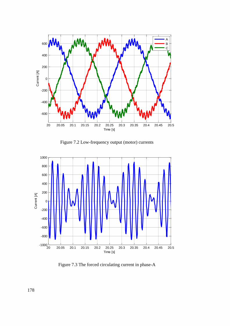
178
Figure 7.2 Low-frequency output (motor) currents
Figure 7.3 The forced circulating current in phase-A
20 20.05 20.1 20.15 20.2 20.25 20.3 20.35 20.4 20.45 20.5
-600
-400
-200
0
200
400
600
Curr
ent
[A]
Time [s]
A
B
C
20 20.05 20.1 20.15 20.2 20.25 20.3 20.35 20.4 20.45 20.5-1000
-800
-600
-400
-200
0
200
400
600
800
1000
Curr
ent
[A]
Time [s]
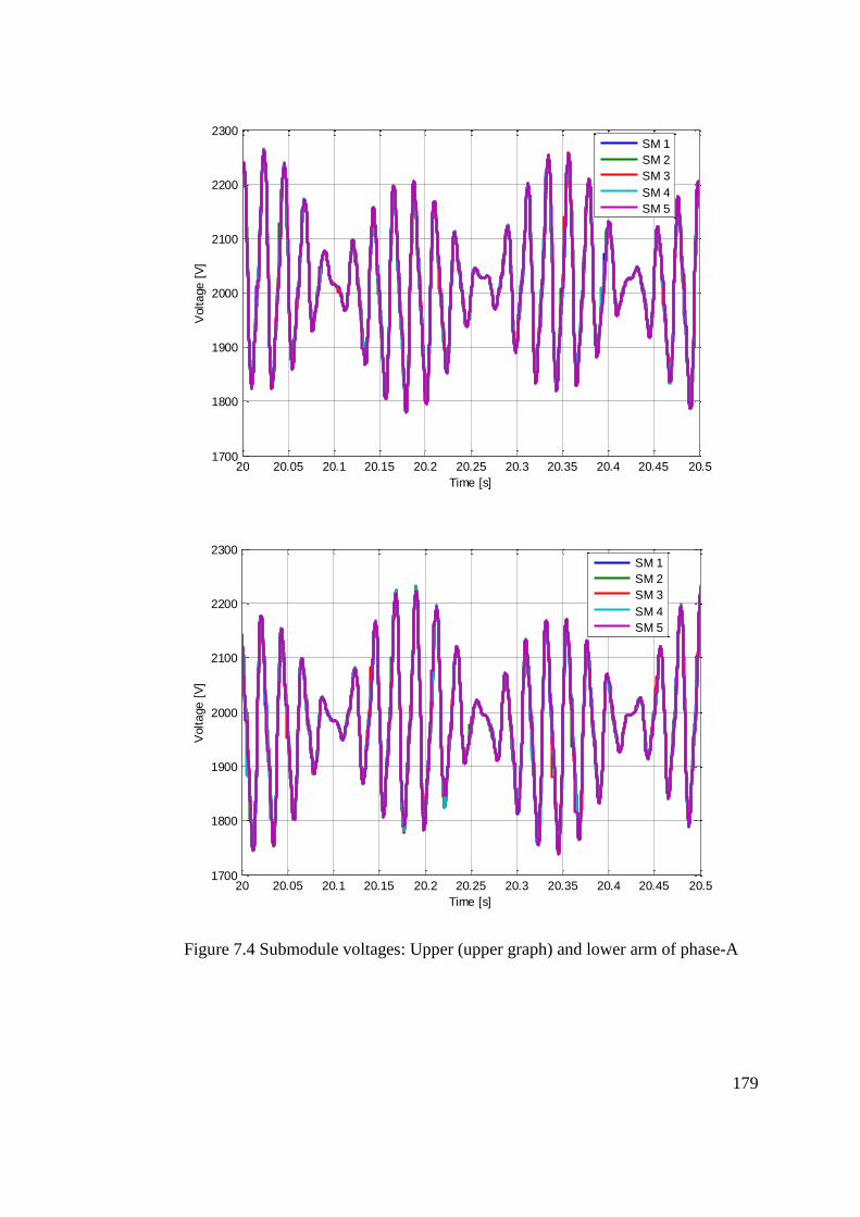
179
Figure 7.4 Submodule voltages: Upper (upper graph) and lower arm of phase-A
20 20.05 20.1 20.15 20.2 20.25 20.3 20.35 20.4 20.45 20.51700
1800
1900
2000
2100
2200
2300
Volt
age
[V
]
Time [s]
SM 1
SM 2
SM 3
SM 4
SM 5
20 20.05 20.1 20.15 20.2 20.25 20.3 20.35 20.4 20.45 20.51700
1800
1900
2000
2100
2200
2300
Volt
age
[V
]
Time [s]
SM 1
SM 2
SM 3
SM 4
SM 5
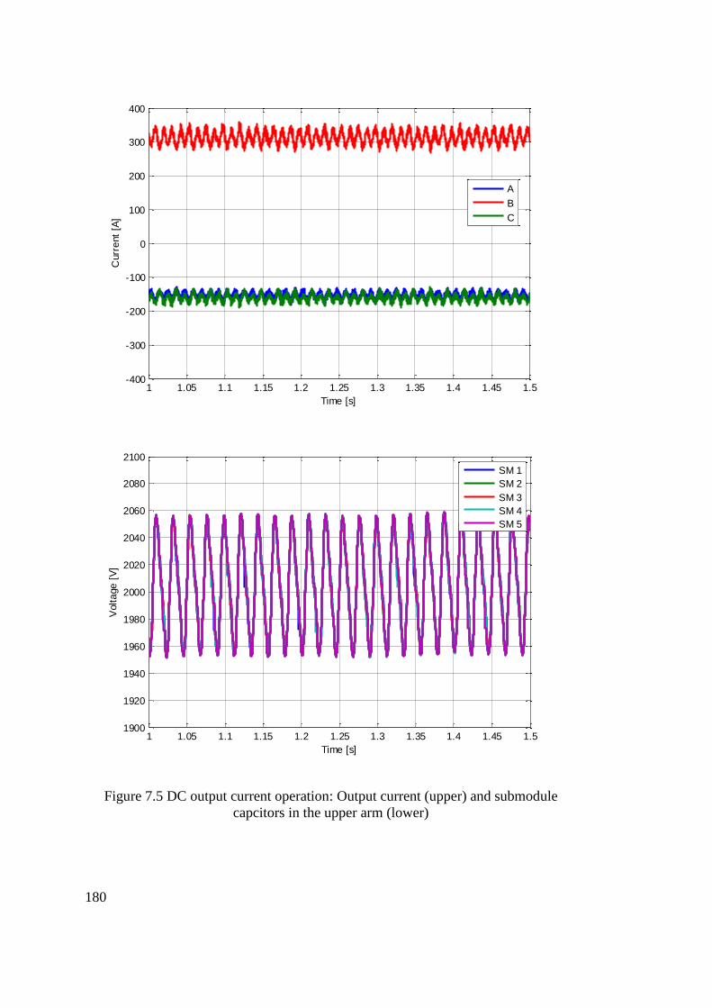
180
Figure 7.5 DC output current operation: Output current (upper) and submodule
capcitors in the upper arm (lower)
1 1.05 1.1 1.15 1.2 1.25 1.3 1.35 1.4 1.45 1.5-400
-300
-200
-100
0
100
200
300
400C
urr
ent
[A]
Time [s]
A
B
C
1 1.05 1.1 1.15 1.2 1.25 1.3 1.35 1.4 1.45 1.51900
1920
1940
1960
1980
2000
2020
2040
2060
2080
2100
Volt
age
[V
]
Time [s]
SM 1
SM 2
SM 3
SM 4
SM 5
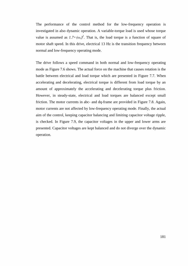
181
The performance of the control method for the low-frequency operation is
investigated in also dynamic operation. A variable-torque load is used whose torque
value is assumed as 1.7×(ωr)2. That is, the load torque is a function of square of
motor shaft speed. In this drive, electrical 13 Hz is the transition frequency between
normal and low-frequency operating mode.
The drive follows a speed command in both normal and low-frequency operating
mode as Figure 7.6 shows. The actual force on the machine that causes rotation is the
battle between electrical and load torque which are presented in Figure 7.7. When
accelerating and decelerating, electrical torque is different from load torque by an
amount of approximately the accelerating and decelerating torque plus friction.
However, in steady-state, electrical and load torques are balanced except small
friction. The motor currents in abc- and dq-frame are provided in Figure 7.8. Again,
motor currents are not affected by low-frequency operating mode. Finally, the actual
aim of the control, keeping capacitor balancing and limiting capacitor voltage ripple,
is checked. In Figure 7.9, the capacitor voltages in the upper and lower arms are
presented. Capacitor voltages are kept balanced and do not diverge over the dynamic
operation.
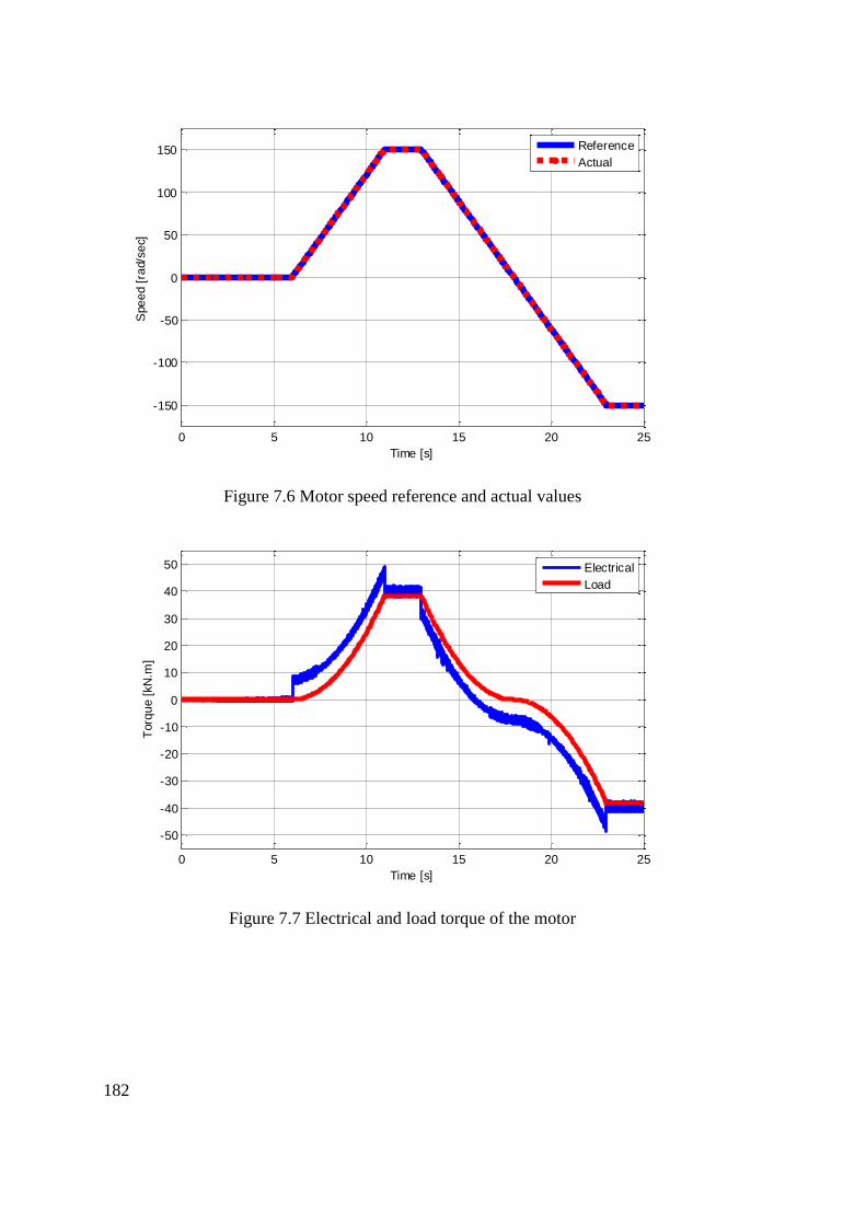
182
Figure 7.6 Motor speed reference and actual values
Figure 7.7 Electrical and load torque of the motor
0 5 10 15 20 25
-150
-100
-50
0
50
100
150S
pe
ed [
rad/s
ec]
Time [s]
Reference
Actual
0 5 10 15 20 25
-50
-40
-30
-20
-10
0
10
20
30
40
50
Torq
ue [
kN
.m]
Time [s]
Electrical
Load
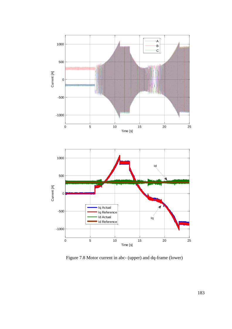
183
Figure 7.8 Motor current in abc- (upper) and dq-frame (lower)
0 5 10 15 20 25
-1000
-500
0
500
1000
Curr
ent
[A]
Time [s]
A
B
C
0 5 10 15 20 25
-1000
-500
0
500
1000
Curr
ent
[A]
Time [s]
Iq Actual
Iq Reference
Id Actual
Id Reference
Id
Iq
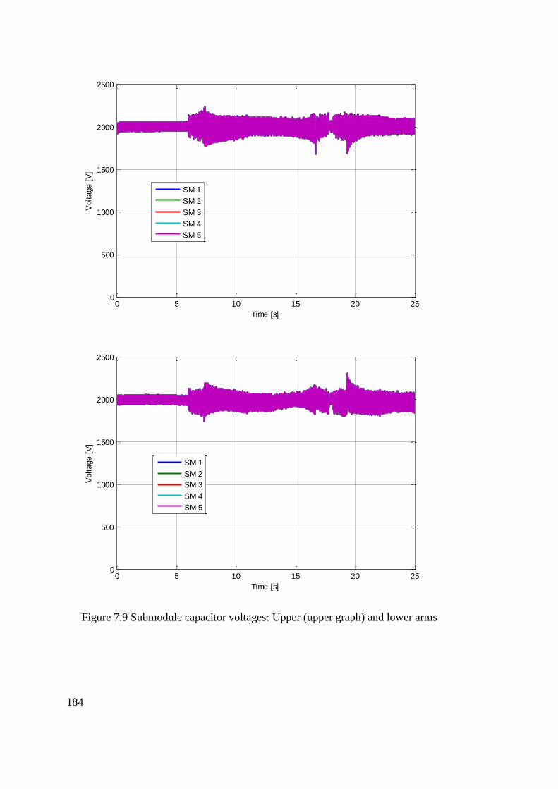
184
Figure 7.9 Submodule capacitor voltages: Upper (upper graph) and lower arms
0 5 10 15 20 250
500
1000
1500
2000
2500V
olt
age
[V
]
Time [s]
SM 1
SM 2
SM 3
SM 4
SM 5
0 5 10 15 20 250
500
1000
1500
2000
2500
Volt
age
[V
]
Time [s]
SM 1
SM 2
SM 3
SM 4
SM 5

185
7.4. Summary
Low-frequency operation of MMC results in large ripples in the submodule capacitor
voltages. To solve this problem, a new control method is shown. This method
requires to use a higher frequency common mode voltage in the arm voltage
references and to force an artificial circulating current. All these shift the frequency
of the capacitor voltage ripple to higher values and also decrease the ripple
amplitudes. The common mode voltage and forced circulating current do not affect
the output electrical parameters. Therefore, they can be considered as part of the
inner control. However, the forced circulating current consumes a portion of MMC
current conduction capacity and similarly the injected common mode voltage also
uses some of the voltage capacity of MMC. That means providing inner stability in
low-frequency region is not cheap. Therefore, less room is left for output current and
voltage in the capacity of MMC to be used for motor. As a result, the achievable
torque at low-frequency operation mode is limited. That being said, the proposed
control approach of low-frequency operation, at least, allows the utilization of MMC
in motor drives. Consequently, MMC based motor drives are considered to be
appropriate for variable torque loads such as fan/blower which need low torque in
low frequencies.
With the help of the low-frequency operation, MMC can supply DC or very low-
frequency current without losing the balance of the submodule capacitor voltages. In
addition, the capacitor voltages do not move away from the average value. In this
way, effectiveness of the control method is verified.
186
CHAPTER 8
8. CONCLUSION
CONCLUSION
While allowing handling higher voltage and power levels, multilevel converters
create lower harmonic distortion. Modular multilevel converter is the unique
example of multilevel converters. It does not need multi-winding and complex
transformer. It can supply active power although its capacitors are floating. Today,
MMC finds applications especially in HVDC field such as connection offshore wind
farm to the power grid in mainland and interconnection of two countries to improve
power system stability.
This thesis focuses on the investigation of modular multilevel converter control
methods.
First of all, the modeling approaches of MMC are presented. The basic model seeks
the differential equations that broadly show the inner dynamics of MMC that define
the control structures to be utilized. Another model is developed on the harmonic
content of the circulating and output current. This is used to show the cyclic relation
among the submodule capacitance voltage, output voltage, output current, and
circulating current. That means all these electrical parameters are coupled in MMC
and affect each other.
Later, all the control aspects of MMC are discussed. The controllers are intuitively
derived from their physics-based dynamic equations. Detailed description of the
MMC control begins with the output current control. Along with vector control
basics, output current control scheme in three-phase VSC is developed and adopted
to MMC case. Similarly, DC-link voltage control as well as output active and

187
reactive power control is explored. Later, the modulation methods suitable for MMC
are reviewed. Phase-shifted and level-shifted PWM methods of carrier based
modulation and nearest level modulation which is appropriate for the MMC designs
with the high number of submodules per arm are reviewed. N+1 and 2N+1 level
voltage generation techniques for carrier based PWM methods are explored. Lastly,
the inner control of MMC, which includes circulating current control and capacitor
voltage balancing, is studied. Capacitor balancing is vital to MMC. Otherwise, it
cannot operate.
The circulating current control eliminates the second-harmonic component in order
to increase efficiency and also to permit the utilization of electrical component with
lower rating. The effectiveness of this control in efficiency improvement is verified
in Chapter 5. Alternatively, the usage of higher submodule capacitance passively
decrease the second-harmonic component of circulating current and hence improves
efficiency. However, it has been shown that the circulating current control is more
effective than increasing the stored energy (the submodule capacitance value) for
reducing the power semiconductor stresses and losses. Thus, the importance of using
such a method as an active control method, rather than suppression of losses by large
passive components is more favorable. Furthermore, the circulating current control
directly changes the arm current. Therefore, the commutated current in the
semiconductors and hence capacitor currents are all affected. As a result, capacitor
voltage ripple decreases. On the other hand, this control does not basically affect the
output side of MMC, but may lower the output voltage THD due to lowered ripple
amplitude of the capacitor voltages.
In this thesis, three sorting algorithms, basic sorting, improved sorting, and RSF
sorting algorithms, are listed with each having gradual improvement. All the three
algorithms first sort the submodule voltages according to their amplitude and then
selects the submodules according to the arm current direction. Therefore, they are all
successful at balancing the submodule capacitor voltages in both steady-state and
dynamic operation. On the other hand, it has also been shown that the sorting
188
algorithm strongly influences the losses and advanced sorting methods provide
significant loss performance enhancements. In the system studied in this thesis, the
improved sorting algorithm is estimated to achieve power loss reduction of 25-35 %
of the conventional method. RSF sorting method further decreases power loss to
approximately 55-65 % of the conventional sorting method in various power factor
and circulating current control conditions studied in this work. Elevated PWM carrier
frequency further increases this importance.
After the comparison of N+1 and 2N+1 level switching techniques, it is concluded
that the latter technique improves waveform quality by shifting the equivalent
switching frequency at the output to two multiples of the previous one. On the other
hand, a harmonic component at the equivalent PWM carrier frequency appears in the
DC-link and circulating current although second-harmonic component of circulating
current is eliminated. N+1 and 2N+1 level switching techniques of three PWM
methods, PD-, PS-, and APOD-PWM, are also compared in terms of voltage
waveform quality. If N+1 level switching technique is selected, then best method is
PD-PWM. The PS- and APOD-PWM methods are apparently worse than PD-PWM.
On the other hand, under 2N+1 level switching technique, all methods have better
and lower THD at the expense of generating a new DC-link and circulating current
harmonic at PWM carrier frequency. In addition, the improvement in PD-PWM is
limited. Furthermore, it may also be expected that 2N+1 level technique may lose its
superiority in waveform quality as the submodule per arm, N, increases.
Additionally, it has been demonstrated that PD- and PS-PWM techniques exhibit no
major performance difference in terms of the total power loss in the converter and
loss distribution among the individual semiconductors.
MMC has an important power loss distribution behavior among the semiconductors.
The individual power losses of the semiconductors in the submodule heavily depend
on power factor. For example, unity power factor, either supplying or consuming
active power, is the worst case for the power loss unbalance. This is attributed to DC
component of circulating current due to the active power transfer. The reason is that
189
DC part of the circulating current creates asymmetry in the arm current and unequal
active time of commutation pair in the submodule. One pair (T1-D2 or T2-D1)
becomes active more than half of the period and also experience higher peak currents
due to the asymmetry in the arm current. Which pair is affected by this situation
depend on the direction of active power transfer. Considering that MMC systems are
likely to operate around unity power factor either rectifier or inverter sides of HVDC
links, this issue requires special attention. However, in reactive power operation, the
commutation pairs in the submodule have nearly equal power loss. Arm current
symmetry is kept because DC part of circulating current is negligible in reactive
power operation.
Back-to-back MMC system, which may be used as HVDC system, does not have
common DC-link capacitor, but each converter independently has submodule
capacitors in place of the common DC-link capacitor. The limitation of classical
back-to-back converter control when employed in the control of back-to-back
connected MMCs is highlighted. Controlling DC-link voltage at rectifier side does
not mean rigid control also at inverter side because the capacitors of the rectifier and
inverter MMCs are separated by the arm and DC-link impedances. Therefore, DC-
link control only by rectifier does not offer good performance in dynamic condition.
As a result, this thesis proposes a new control method targeting this problem. Both
converters should independently regulate the average voltage of its own submodule
capacitors. However, in addition to this, DC-part of circulating current is also
regulated by adjusting DC-link equivalent voltage of inverter side. That means the
proposed control has two parts. First one is to control average voltages of all
capacitors at "both" rectifier and inverter side independently. Second part is to
control DC-link equivalent voltage of "only" one side, possibly inverter side, through
control of DC part of circulating current. In this way, regardless of loading level and
voltage drop between converters, all capacitor voltage are regulated to same voltage
and also oscillatory dynamics are eliminated.
190
Low-frequency operation of MMC may cause large voltage ripple in the submodule
capacitor voltages. A special control method which is effective in a pre-defined low-
frequency operation region is presented to solve this problem. This method uses a
higher-frequency common-mode voltage in the arm voltage references and also
forces an artificial circulating-current. All these shift the frequency of capacitor
voltage ripple to higher values, therefore; lower the ripple amplitudes. The common
mode voltage and forced circulating current ideally do not affect the output electrical
parameters. Therefore, they can be considered as part of the inner control. However,
the circulating current uses a current capacity of MMC and similarly the injected
common mode voltage also exploits some of the voltage generating capacity of
MMC. Therefore, less room is left for output current and voltage in the capacity of
MMC to be used for motor. That means the achievable torque at low-frequency
operation mode is limited. That being said, the proposed control approach of low-
frequency operation, at least, allows the utilization of MMC in motor drives. As a
result, MMC based motor drives are considered to be appropriate for variable torque
loads such as fan/blower which need low torque in low frequencies. With the help of
the low-frequency operation mode, MMC can supply DC or very low-frequency
current without losing the balance of the submodule capacitor voltages. In addition,
the capacitor voltages do not move away from the average value. In this way,
effectiveness of the control method is verified.
As a potential future work, the control techniques studied here may be extended to
cover the MMC behavior under unbalanced grid and fault conditions.
191
REFERENCES
[1] T. J. Hammons, D. Woodford, J. Loughtan, M. Chamia, J. Donahoe, D. Povh,
B. Bisewski, and W. Long, "Role of HVDC transmission in future energy
development," Power Engineering Review, IEEE, vol.20, no.2, pp.10-25, Feb
2000.
[2] Mitsubishi, “HVIGBT Modules” [online] Available:
http://www.mitsubishielectric.com/semiconductors/products/powermod/hvig
btmod/index.html [Accessed: April, 2015]
[3] P. W. Hammond, “A new approach to enhance power quality for medium
voltage AC drives,” Industry Applications, IEEE Transactions on, vol.33,
no.1, pp.202-208, Jan./Feb. 1997.
[4] F. Z. Peng, J. Lai, J. W. McKeever, and J. VanCoevering, “A multilevel
voltage-source inverter with separate DC sources for static VAr generation,”
Industry Applications, IEEE Transactions on, vol.32, no.5, pp.1130-1138,
Sep./Oct. 1996.
[5] H. Akagi, “Classification, terminology, and application of the modular
multilevel cascade converter (MMCC),” Power Electronics, IEEE
Transactions on, vol.26, no.11, pp.3119-3130, Nov. 2011.
[6] R. Marquardt and A. Lesnicar “A new modular voltage source inverter
topology,” in Conf. Rec. Eur. Conf. Power Electron. Appl., 2003, pp. 1–10.
[CD-ROM].
[7] M. Davies, M. Dommaschk, J. Dorn, J. Lang, D. Retzmann, and D. Soerangr,
"HVDC Plus - Basics and Principle of Operation" [online] Available:
http://www.energy.siemens.com/br/pool/br/transmissao-de-
energia/transformadores/hvdc-plus-basics-and-principle-of-operation.pdf,
[Accessed: April, 2015].

192
[8] N. Flourentzou, V. G. Agelidis, G. D. Demetriades, “VSC-based HVDC
power transmission systems: An overview,” Power Electronics, IEEE
Transactions on, vol.24, no.3, pp.592-602, Mar. 2009.
[9] ABB, "HVDC Light® It's time to connect," [online] Available:
http://www05.abb.com/global/scot/scot221.nsf/veritydisplay/2742b98db321b
5bfc1257b26003e7835/$file/Pow0038%20R7%20LR.pdf, [Accessed: April,
2015].
[10] ALSTOM, "HVDC-VSC: Transmission technology of the future," [online]
Available:
http://www.alstom.com/Global/CleanGrid/Resources/Documents/HVDC-
VSC%20transmission%20technology%20of%20the%20future%20-
%20Think%20Grid%20n%C2%B08%20.pdf, [Accessed: April, 2015].
[11] N. Serbia, "Modular multilevel converters for HVDC power stations," Ph.D.
dissertation, Institut National Polytechnique de Toulouse, 2014.
[12] Siemens “Siemens Debuts HVDC PLUS with San Francisco’s Trans Bay
Cable” [online] Available:
http://www.energy.siemens.com/hq/pool/hq/energy-topics/living-
energy/issue-5/livingenergy_05_hvdc.pdf [Accessed: April, 2015]
[13] Federal Ministry for Economic Affairs and Energy, “Wind Farms” [online]
Available: http://www.offshore-windenergie.net/en/wind-farms, [Accessed:
May, 2015]
[14] M. A. Perez, S. Bernet, J. Rodriguez, and S. Kouro, "Circuit Topologies,
Modeling, Control Schemes, and Applications of Modular Multilevel
Converters," Power Electronics, IEEE Transactions on, vol.30, no.1, pp.4-17,
Jan 2015.
[15] P. L. Francos, S. S. Verdugo, H. F. Alvarez, and S. Guyomarch, “INELFE –
Europe’s first integrated onshore HVDC interconnection”, Power and Energy
Society General Meeting, 2012 IEEE, pp.1-8, Jul 2012.
193
[16] WEG “Medium Voltage Industrial Variable Speed Drives” [online]
Available: http://ecatalog.weg.net/files/wegnet/WEG-medium-voltage-
industrial-variable-speed-drives-technical-article-english.pdf [Accessed:
April, 2015]
[17] M. Hagiwara, K. Nishimura, and H. Akagi, “A medium-voltage motor drive
with a modular multilevel PWM inverter,” Power Electronics, IEEE
Transactions on, vol.25, no.7, pp.1786-1799, Jul. 2010.
[18] BENSAW “M2L 3000 Series Medium Voltage Variable Frequency Drive”
[online] Available: http://www.benshaw.com/pdf/125-
009_RevB_MVVFD_M2L_3000_Series.pdf [Accessed: April, 2015]
[19] SIEMENS, "SVC PLUS (VSC Technology)" [online] Available:
http://www.energy.siemens.com/hq/en/power-transmission/facts/static-var-
compensator-plus/converter.htm#content=Description, [Accessed: April,
2014].
[20] ABB, "SVC Light® The next generation," [online] Available:
http://www02.abb.com/global/gad/gad02181.nsf/0/4baf00331add08d1c1257a
62003102d3/$file/SVC+Light+-+The+next+generation.pdf, [Accessed: April,
2014].
[21] K. Ilves, A. Antonopoulos, S. Norrga, and H. P. Nee, “Steady-state analysis
of interaction between harmonic components of arm and line quantities of
modular multilevel converters,” Power Electronics, IEEE Transactions on,
vol.27, no.1, pp.57-68, Jan. 2012.
[22] A. J. Korn, M. Winkelnkemper, and P. Steimer, “Low output frequency
operation of the modular multi-level converter,” Energy Conversion
Congress and Exposition (ECCE), 2010 IEEE, pp. 3993 – 3997, 12-16 Sept.
2010.
[23] A. Antonopoulos, L. Angquist, and H.-P. Nee, "On dynamics and voltage
control of the Modular Multilevel Converter," Power Electronics and
194
Applications, 2009. EPE '09. 13th European Conference on, pp.1-10, 8-10
Sept. 2009.
[24] B. Gültekin and M. Ermiş, “Cascaded multilevel converter-based
transmission STATCOM: System design methodology and development of a
12 kV ±12 MVAr power stage,” Power Electronics, IEEE Transactions on,
vol.28, no.11, pp.4930-4950, Nov. 2013.
[25] Q. Tu, Z. Xu, and L. Xu, “Reduced switching-frequency modulation and
circulating current suppression for modular multilevel converters,” Power
Delivery, IEEE Transactions on, vol.26, no.3, pp.2009-2017, Jul. 2011.
[26] B. Jacobson, P. Karlsson, G. Asplund, L. Harnefors, and T. Jonsson, "VSC-
HVDC transmission with cascaded two-level converters," Cigré session,
2010.
[27] J. Peralta, H. Saad, S. Dennetiere, J. Mahseredjian, and S. Nguefeu, “Detailed
and averaged models for a 401-level MMC–HVDC system,” Power Delivery,
IEEE Transactions on, vol.27, no.3, pp.1501-1508, Jul. 2012.
[28] Q. Tu, Z. Xu, and H. Huang, “Parameter design principle of the arm inductor
in modular multilevel converter based HVDC,” Power System Technology
(POWERCON), 2010 International Conference on, pp. 1-6, 24-28 Oct. 2010.
[29] M. Glinka and R. Marquardt, “A new single-phase ac/ac-multilevel converter
for traction vehicles operating on ac line voltage,” Power Tech Conference
Proceedings,2003 IEEE Bologna, vol.3, pp.6 , 23-26 June 2003.
[30] M. Hagiwara, R. Maeda, and H. Akagi, “Control and Analysis of the modular
multilevel cascade converter based on double-star chopper-cells (MMCC-
DSCC),” Power Electronics, IEEE Transactions on, vol.26, no.6, pp.1649-
1658, Jun. 2011.
195
[31] F. Ertürk, B. Ciftci, and A. Hava, "Modüler çok seviyeli dönüştürücülerin
kontrolü," ELECO 2014, Elektrik - Elektronik - Bilgisayar Mühendisliği
Sempozyumu, 27-29 November 2014, Bursa, pp. 256-262.
[32] B. Ciftci, F. Ertürk, and A. Hava, "Modüler çok seviyeli dönüştürücülerde
taşıyıcı temelli DGM ile anahtarlama ve kondansatör gerilimi dengeleme
yöntemleri," ELECO 2014, Elektrik - Elektronik - Bilgisayar Mühendisliği
Sempozyumu, 27-29 November 2014, Bursa, pp. 250-255.
[33] J. K. Seok, J. S. Kim, and S. K. Sul, “Overmodulation strategy for high-
performance torque control,” Power Electronics, IEEE Transactions on,
vol.13, no.4, pp.786-792, Jul. 1998.
[34] V. Kaura and V. Blasko, “Operation of a phase locked loop system under
distorted utility conditions,” Industry Applications, IEEE Transactions on,
vol.33, no.1, pp.58-63, Jan/Feb. 1997.
[35] V. Blasko and V. Kaura, “A new mathematical model and control of a three-
phase AC–DC voltage source converter,” Power Electronics, IEEE
Transactions on, vol.12, no.1, pp.786-792, Jan. 1997.
[36] K. Sekiguchi, P. Khamphakdi, M. Hagiwara, and H. Akagi, “A grid-level
high-power BTB (Back-To-Back) system using modular multilevel cascade
converters without common DC-link capacitor,” Industry Applications, IEEE
Transactions on, vol.50, no.4, pp.2648-2659, Jul/Aug. 2014.
[37] M. Zhang, L. Huang, W. Yao, and Z. Lu, “Circulating harmonic current
elimination of a CPS-PWM-based modular multilevel converter with a plug-
in repetitive controller,” Power Electronics, IEEE Transactions on, vol.29,
no.4, pp.2083-2097, Apr. 2014.
[38] X. She, A. Huang, X. Ni, and R. Burgos, “AC Circulating Currents
Suppression in Modular Multilevel Converter,” IECON 2012 - 38th Annual
Conference on IEEE Industrial Electronics Society, pp.191–196,25-28 Oct.
2012.
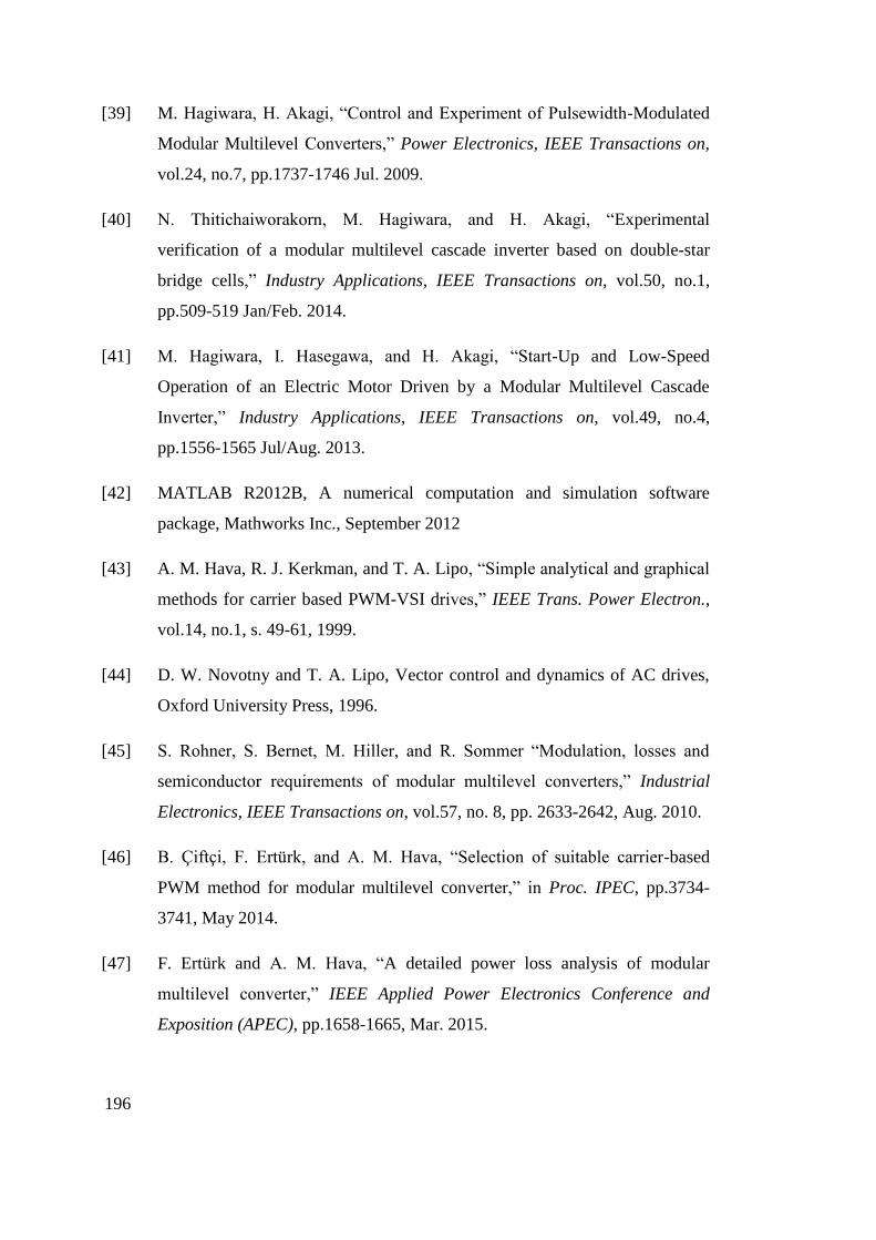
196
[39] M. Hagiwara, H. Akagi, “Control and Experiment of Pulsewidth-Modulated
Modular Multilevel Converters,” Power Electronics, IEEE Transactions on,
vol.24, no.7, pp.1737-1746 Jul. 2009.
[40] N. Thitichaiworakorn, M. Hagiwara, and H. Akagi, “Experimental
verification of a modular multilevel cascade inverter based on double-star
bridge cells,” Industry Applications, IEEE Transactions on, vol.50, no.1,
pp.509-519 Jan/Feb. 2014.
[41] M. Hagiwara, I. Hasegawa, and H. Akagi, “Start-Up and Low-Speed
Operation of an Electric Motor Driven by a Modular Multilevel Cascade
Inverter,” Industry Applications, IEEE Transactions on, vol.49, no.4,
pp.1556-1565 Jul/Aug. 2013.
[42] MATLAB R2012B, A numerical computation and simulation software
package, Mathworks Inc., September 2012
[43] A. M. Hava, R. J. Kerkman, and T. A. Lipo, “Simple analytical and graphical
methods for carrier based PWM-VSI drives,” IEEE Trans. Power Electron.,
vol.14, no.1, s. 49-61, 1999.
[44] D. W. Novotny and T. A. Lipo, Vector control and dynamics of AC drives,
Oxford University Press, 1996.
[45] S. Rohner, S. Bernet, M. Hiller, and R. Sommer “Modulation, losses and
semiconductor requirements of modular multilevel converters,” Industrial
Electronics, IEEE Transactions on, vol.57, no. 8, pp. 2633-2642, Aug. 2010.
[46] B. Çiftçi, F. Ertürk, and A. M. Hava, “Selection of suitable carrier-based
PWM method for modular multilevel converter,” in Proc. IPEC, pp.3734-
3741, May 2014.
[47] F. Ertürk and A. M. Hava, “A detailed power loss analysis of modular
multilevel converter,” IEEE Applied Power Electronics Conference and
Exposition (APEC), pp.1658-1665, Mar. 2015.
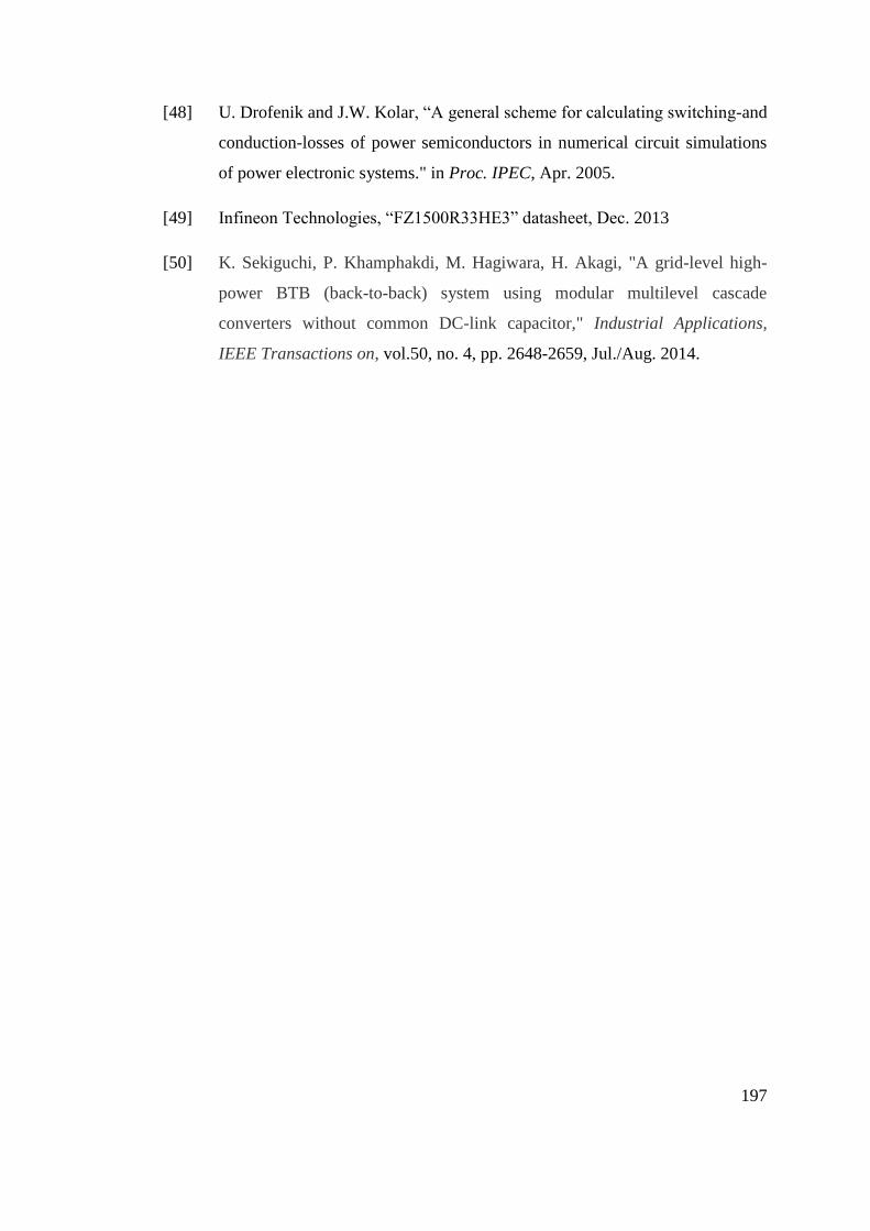
197
[48] U. Drofenik and J.W. Kolar, “A general scheme for calculating switching-and
conduction-losses of power semiconductors in numerical circuit simulations
of power electronic systems." in Proc. IPEC, Apr. 2005.
[49] Infineon Technologies, “FZ1500R33HE3” datasheet, Dec. 2013
[50] K. Sekiguchi, P. Khamphakdi, M. Hagiwara, H. Akagi, "A grid-level high-
power BTB (back-to-back) system using modular multilevel cascade
converters without common DC-link capacitor," Industrial Applications,
IEEE Transactions on, vol.50, no. 4, pp. 2648-2659, Jul./Aug. 2014.

198
199
APPENDIX
A. APPENDIX Below, MATLAB/Simulink simulation models utilized in this thesis are presented.
(a) Simulation overview
(b) MMC block
Figure A.1 MMC model for Chapter 4
200
(a) Control blocks
(b) Sorting algorithm blocks
Figure A.2 MMC controller model
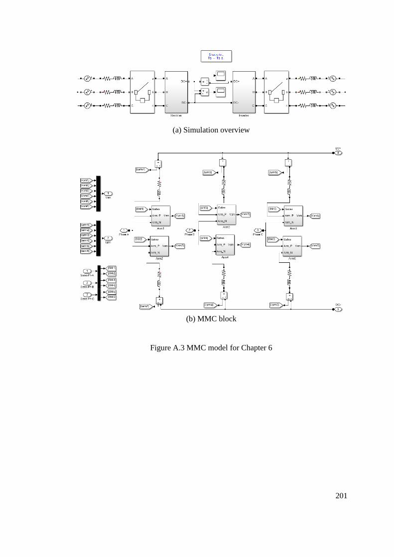
201
(a) Simulation overview
(b) MMC block
Figure A.3 MMC model for Chapter 6

202
Figure A.4 Simulation overview for Chapter 7