inventions represented at danish ip fair 2018 · the novel precious metal recovery method has been...
TRANSCRIPT

Advanced Materials and Technologies
Inventions represented at Danish IP Fair 2018Advanced Materials and Technologies
This document contains one-pagers for all inventions within Advanced Materials andTechnologies presented at the Danish IP Fair 2018. You can use this document toidentify meeting partners at the event. Each invention is marked with a unique ID atthe top right of the page. Use this ID to look up and book a meeting with theinventor(s) at the Danish IP Fair website - www.dipfair.dk.
The document will be updated regularly in the period February-April, so ensure to re-visit the website for the newest version.
For further guidelines regarding meeting bookings please consult the menuMatchmaking on the website.
Device and method for detecting and imaging conductive objects
Advanced Materials and Technologies
Value Proposition• Our device can detect and image electrically conductive objects.• The method is non-destructive. The device is placed at a distance from the object to be imaged.• Key features: improved signal-to-noise ratio and high sensitivity => fast detection of high and low conductivity objects.
Commercial PerspectivesDetection, imaging and characterisation of conductive objects is of interest for• industry, for detecting cracks or defects in surfaces of metals or other high-conductivity materials• geophysics, for underground exploration and localisation of hidden objects• bio-medical devices, for imaging biological tissue (including the heart), potentially a tool for medical diagnostics.
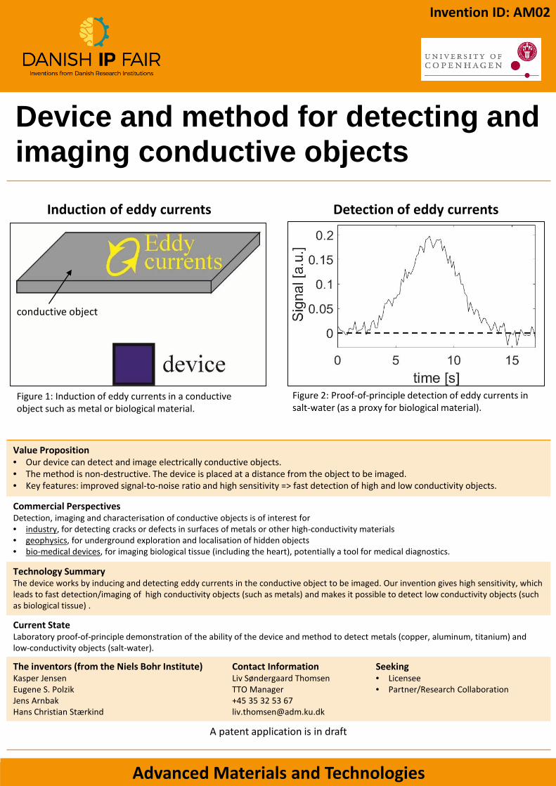
Technology SummaryThe device works by inducing and detecting eddy currents in the conductive object to be imaged. Our invention gives high sensitivity, which leads to fast detection/imaging of high conductivity objects (such as metals) and makes it possible to detect low conductivity objects (such as biological tissue) .
Current StateLaboratory proof-of-principle demonstration of the ability of the device and method to detect metals (copper, aluminum, titanium) and low-conductivity objects (salt-water).
The inventors (from the Niels Bohr Institute)Kasper Jensen Eugene S. PolzikJens ArnbakHans Christian Stærkind
Contact InformationLiv Søndergaard ThomsenTTO Manager+45 35 32 53 67 [email protected]
Seeking• Licensee• Partner/Research Collaboration
A patent application is in draft
Invention ID: AM02
Figure 2: Proof-of-principle detection of eddy currents in salt-water (as a proxy for biological material).
Detection of eddy currents
conductive object
Figure 1: Induction of eddy currents in a conductive object such as metal or biological material.
Induction of eddy currents
Photoactive Pigments:Luminescent and photochromic inorganic pigments made from cheap, non-toxic and abundant raw materials
Advanced Materials and Technologies
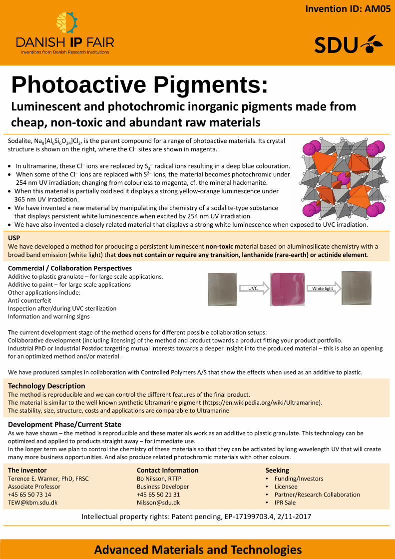
Sodalite, Na8[Al6Si6O24]Cl2, is the parent compound for a range of photoactive materials. Its crystalstructure is shown on the right, where the Cl− sites are shown in magenta.
• In ultramarine, these Cl− ions are replaced by S3− radical ions resulting in a deep blue colouration.
• When some of the Cl− ions are replaced with S2− ions, the material becomes photochromic under 254 nm UV irradiation; changing from colourless to magenta, cf. the mineral hackmanite.
• When this material is partially oxidised it displays a strong yellow-orange luminescence under 365 nm UV irradiation.
• We have invented a new material by manipulating the chemistry of a sodalite-type substancethat displays persistent white luminescence when excited by 254 nm UV irradiation.
• We have also invented a closely related material that displays a strong white luminescence when exposed to UVC irradiation.
USPWe have developed a method for producing a persistent luminescent non-toxic material based on aluminosilicate chemistry with a broad band emission (white light) that does not contain or require any transition, lanthanide (rare-earth) or actinide element.
Commercial / Collaboration PerspectivesAdditive to plastic granulate – for large scale applications.Additive to paint – for large scale applicationsOther applications include:Anti-counterfeitInspection after/during UVC sterilizationInformation and warning signs
The current development stage of the method opens for different possible collaboration setups:Collaborative development (including licensing) of the method and product towards a product fitting your product portfolio.Industrial PhD or Industrial Postdoc targeting mutual interests towards a deeper insight into the produced material – this is also an opening for an optimized method and/or material.
We have produced samples in collaboration with Controlled Polymers A/S that show the effects when used as an additive to plastic.
Technology DescriptionThe method is reproducible and we can control the different features of the final product.The material is similar to the well known synthetic Ultramarine pigment (https://en.wikipedia.org/wiki/Ultramarine).The stability, size, structure, costs and applications are comparable to Ultramarine
Development Phase/Current StateAs we have shown – the method is reproducible and these materials work as an additive to plastic granulate. This technology can be optimized and applied to products straight away – for immediate use.In the longer term we plan to control the chemistry of these materials so that they can be activated by long wavelength UV that will create many more business opportunities. And also produce related photochromic materials with other colours.
The inventorTerence E. Warner, PhD, FRSCAssociate Professor+45 65 50 73 [email protected]
Contact InformationBo Nilsson, RTTPBusiness Developer+45 65 50 21 [email protected]
Seeking• Funding/Investors• Licensee• Partner/Research Collaboration• IPR Sale
Intellectual property rights: Patent pending, EP-17199703.4, 2/11-2017
UVC White light
Invention ID: AM05

Value Proposition/USPNanotechnology can be applied to create highly sophisticated custom-made stamps, which could be used on hard surfaces such as metal and plastic with decorative or functional purposes. Case 1: Nanostamping tool is a unique easy to use nanopattern transfer device dedicated for encrypted and design pattern transfer on solid surfaces. This technology competes with conventional stamping tools that create simple patters and holographic technology. However, both competing solutions are either suffer from easy to reproduce options to highly expensive and limited access. Incontrast, we offer a tool that could be fully customized, has an affordable price (stamps per items) and guarantee unique protection or design to your product. Case 2: Direct laser patterning micro- and nanopatterning technology allows to creating a visual pattern on different surfaces with encoded customized designs with high resolution on a variety of surfaces and shapes, including metal, stones with odd shapes or on a flat surface with the minimum size of a dot of below 1 micrometer. The advantage of this technology is fast transfer of patterns on desired surfaces, but the disadvantage is a large amount of investments into a laser system. For that reason we provide an easy to access nanostamping tool, that does not require large initial investments and can be customized and premade according to your needs. Both solutions were specifically designed for jewelry market. We tested both technologies on most of soft metals, meaning a possibility to apply this tool on many products with possibility to protect it and add unique design and value for your business.
Business Opportunity/Objective/Commercial PerspectivesBoth technologies can be used in all industries were products need authenticity or certification protection, physical data protection and as a bonus unique pattern design. Potentially, we consider jewelry and luxury product market, logistics, machine buildings, medical devices etc. Existing authenticity and brand protection technologies do not provide high level of protection, however our solution uses state of the art nanotechnology patterning and encrypting that guarantee impossible reproducibility by third parties.
Technology Description/Technology SummaryBoth technologies have passed successfully prototyping stage and currently considered for customers tests and market access. Bothtechnologies are state of the art developed at DTU with academic and industrial partners.
Development Phase/Current StateBothe technologies are in the process of notification of invetions discussions with partners and DTU.
The inventorsMaksym Plakhotnyuk [email protected]
Contact InformationMaksym Plakhotnyuk TTO Manager+45 27 57 50 92, [email protected]
Seeking• Funding/Investors• Partner/Research Collaboration• IPR Sale
Nanopattern and Protectyour product as easy as a postal stamp or point a laser
Advanced Materials and Technologies
Invention ID: AM06

Recovery of Precious Metals- Environmentally friendly, economic and efficient technologies to recycle precious metals from spent products
Advanced Materials and Technologies
Value PropositionPrecious metals, including Platinum (Pt), Palladium (Pd), Ruthenium (Ru), Iridium (Ir), Rhodium (Rh), Osmium (Os), Silver (Ag) and Gold (Au), are essential materials for many industries, including automotive, jewelry, investment, electronic, chemical, medical, catalysis, everyday products, as well as renewable energy business. In general, one quarter of all goods manufactured either contain a PM or had a PM play a key role in its production. Take Pt & Pd as an example, their annual demand is more than 570 ton per year.
Commercial PerspectivesPrecious metals (PMs) are limited natural resources of tremendous industrial importance. Recovery of PMs is essential to stabilize market supply and be independent of geological & geopolitical restrictions. The global recycling market for PMs is expected to expand 8.2% by 2018 and have a market value of $9 billion.
Technology DescriptionThe classical methods to recycle Precious metals (PMs) require high energy consumption and have a large environmental impact due to the use of hazardous chemicals and/or releasing large amounts of greenhouse gases. The current inventions describes a method to dissolve PM in mild conditions through surface treatment with variation of surface potential. The recovered PM product can be either PM compounds (in form of solution or powder) or metallic form. The technology is environmentally friendly, low cost, efficient, flexible and readily adaptable for large-scale commercialization.
Current StateThe novel precious metal recovery method has been repeatedly confirmed in the lab for small scale production. The inventors continually optimize the treatment conditions, reduce the overall cost, place the subject to the frontier of the scientific studies and utilize stat-of-the-art instrumentations to further clarify reaction mechanisms. A series of patent applications is under processing. Medium and larger scale PM recovery production is under planning.
The inventorsShuang MA Andersen, PhDAssociate [email protected], +45 6550 9186
Raghunandan Sharma, [email protected], +45 6550 8672
Contact InformationBo Nilsson, RTTPBusiness Developer+45 65 50 21 [email protected]
Seeking• Funding/Investors• Licensee• Partner/Research Collaboration• IPR Sale
Intellectual property rights: Patent Pending, April 2018
Invention ID: AM07
Value Proposition/USPThis technology enables the use of switched-capacitor power converters in higher voltage and power levels than used today and eliminates the use of inductors. It shows the potential of better performance than state of the art in power efficiency, power density, electromagneticinterference and cost.
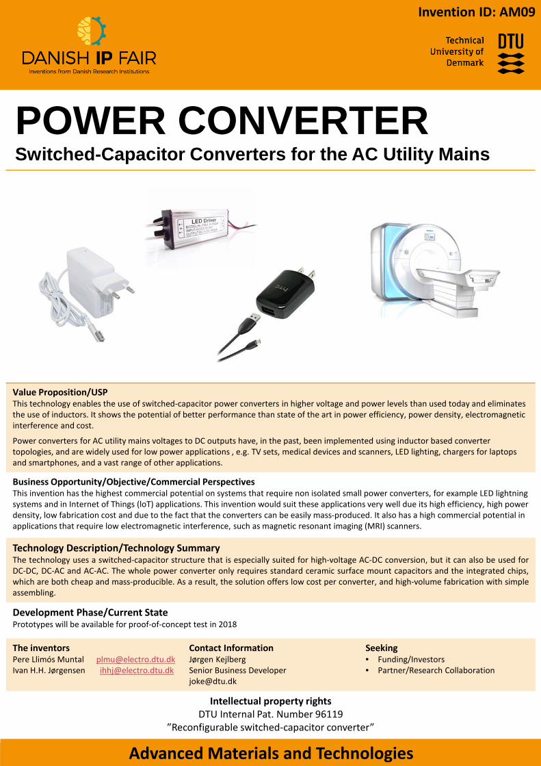
Power converters for AC utility mains voltages to DC outputs have, in the past, been implemented using inductor based converter topologies, and are widely used for low power applications , e.g. TV sets, medical devices and scanners, LED lighting, chargers for laptops and smartphones, and a vast range of other applications.
Business Opportunity/Objective/Commercial PerspectivesThis invention has the highest commercial potential on systems that require non isolated small power converters, for example LED lightning systems and in Internet of Things (loT) applications. This invention would suit these applications very well due its high efficiency, high power density, low fabrication cost and due to the fact that the converters can be easily mass-produced. It also has a high commercial potential in applications that require low electromagnetic interference, such as magnetic resonant imaging (MRI) scanners.
Technology Description/Technology SummaryThe technology uses a switched-capacitor structure that is especially suited for high-voltage AC-DC conversion, but it can also be used forDC-DC, DC-AC and AC-AC. The whole power converter only requires standard ceramic surface mount capacitors and the integrated chips,which are both cheap and mass-producible. As a result, the solution offers low cost per converter, and high-volume fabrication with simpleassembling.
Development Phase/Current StatePrototypes will be available for proof-of-concept test in 2018
The inventorsPere Llimós Muntal [email protected] H.H. Jørgensen [email protected]
Contact InformationJørgen KejlbergSenior Business [email protected]
Seeking• Funding/Investors• Partner/Research Collaboration
Intellectual property rights DTU Internal Pat. Number 96119
”Reconfigurable switched-capacitor converter”
POWER CONVERTERSwitched-Capacitor Converters for the AC Utility Mains
Advanced Materials and Technologies
Invention ID: AM09