introduction to vlsi programming tu/e course 2in30johanl/educ/2in30/vlsip2005-1.pdf · • learn to...
TRANSCRIPT

Introduction to VLSI Programming
TU/e course 2IN30
Prof.dr.ir. Kees van BerkelDr. Johan Lukkien[Dr.ir. Ad Peeters, Philips Nat.Lab]
Philips Research, Kees van Berkel, 2003-09-03 2
TU/e
Introduction to VLSI ProgrammingGoals
• Create silicon (CMOS) awareness• Understanding the metrics for
– Time (speed, performance)– Energy (power consumption)– Area (cost)
• Learn to design at VLSI-programming level– Based on metrics– Tangram silicon compiler is used as a vehicle
Philips Research, Kees van Berkel, 2003-09-03 3
TU/e
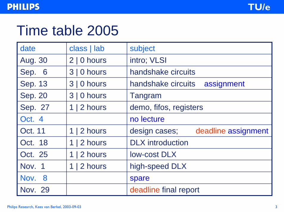
Time table 2005date class | lab subjectAug. 30 2 | 0 hours intro; VLSISep. 6 3 | 0 hours handshake circuits Sep. 13 3 | 0 hours handshake circuits assignmentSep. 20 3 | 0 hours TangramSep. 27 1 | 2 hours demo, fifos, registersOct. 4 no lectureOct. 11 1 | 2 hours design cases; deadline assignmentOct. 18 1 | 2 hours DLX introductionOct. 25 1 | 2 hours low-cost DLXNov. 1 1 | 2 hours high-speed DLXNov. 8 spareNov. 29 deadline final report
Philips Research, Kees van Berkel, 2003-09-03 4
TU/e
Course grading
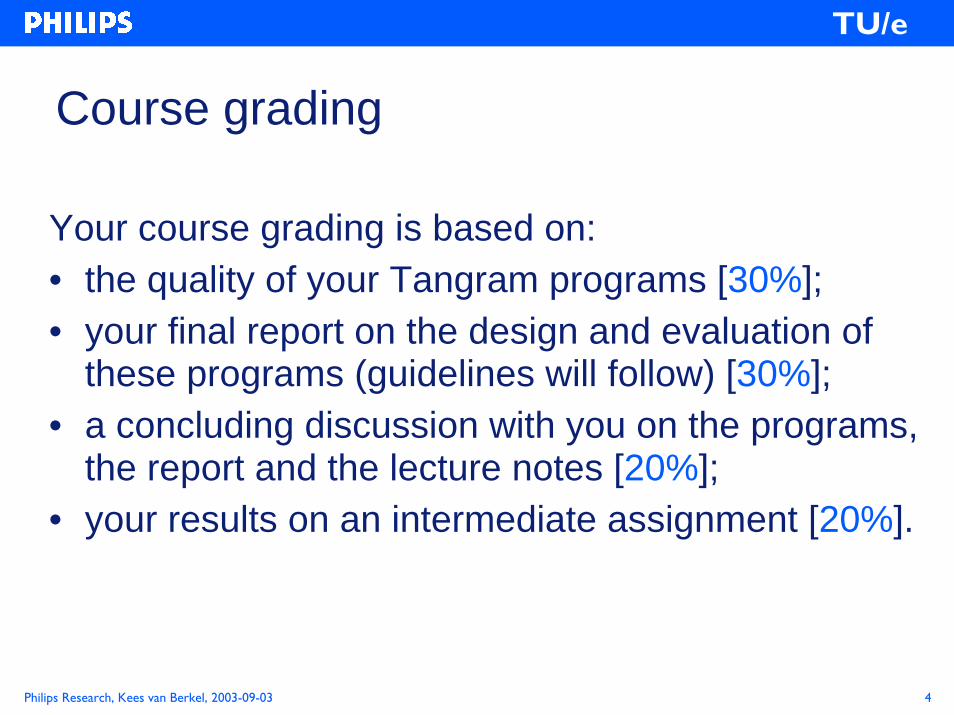
Your course grading is based on:• the quality of your Tangram programs [30%];• your final report on the design and evaluation of
these programs (guidelines will follow) [30%]; • a concluding discussion with you on the programs,
the report and the lecture notes [20%];• your results on an intermediate assignment [20%].

Philips Research, Kees van Berkel, 2003-09-03 5
TU/e
Lecture 1: outline
• ICs, Moore’s Law, ITRS roadmap • VLSI design and silicon compilation• Tangram Handshake Technology• VLSI circuits: basics, metrics, scaling • Abstractions:
– Transistors– Production rules– Gates
Philips Research, Kees van Berkel, 2003-09-03 6
TU/e
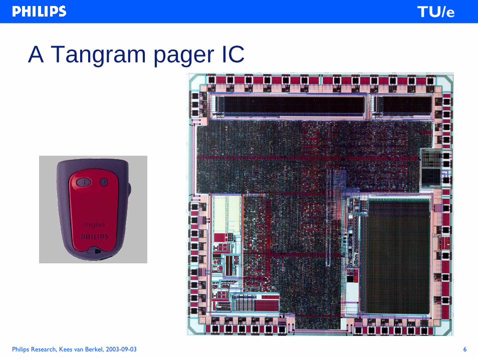
A Tangram pager IC

Philips Research, Kees van Berkel, 2003-09-03 7
TU/e
A Tangram smartcard IC
Philips Research, Kees van Berkel, 2003-09-03 8
TU/e
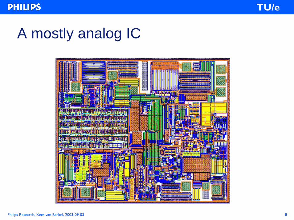
A mostly analog IC
Philips Research, Kees van Berkel, 2003-09-03 9
TU/e
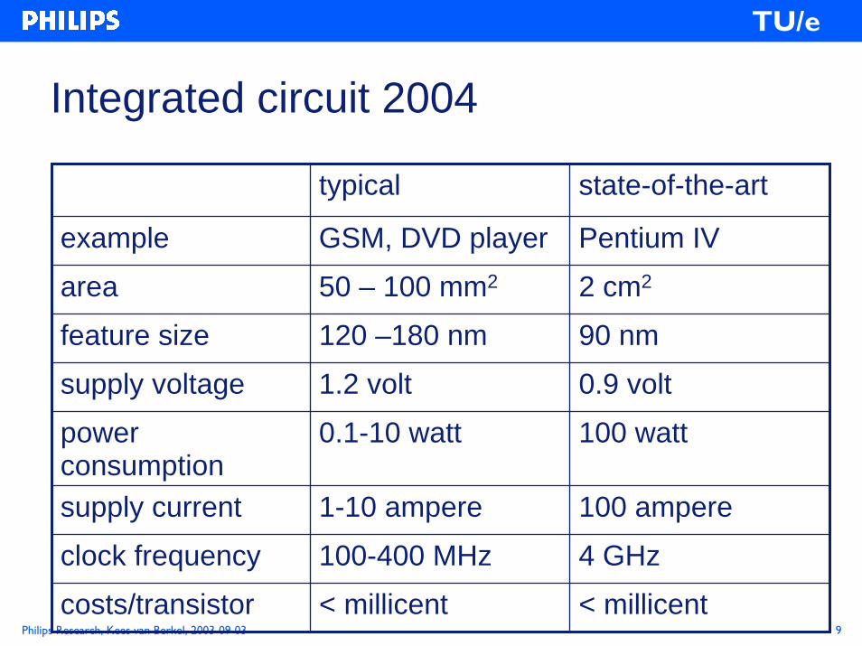
Integrated circuit 2004
typical state-of-the-art
example GSM, DVD player Pentium IV
area 50 – 100 mm2 2 cm2
feature size 120 –180 nm 90 nm
supply voltage 1.2 volt 0.9 volt
power consumption
0.1-10 watt 100 watt
supply current 1-10 ampere 100 ampere
clock frequency 100-400 MHz 4 GHz
costs/transistor < millicent < millicent
Philips Research, Kees van Berkel, 2003-09-03 10
TU/e
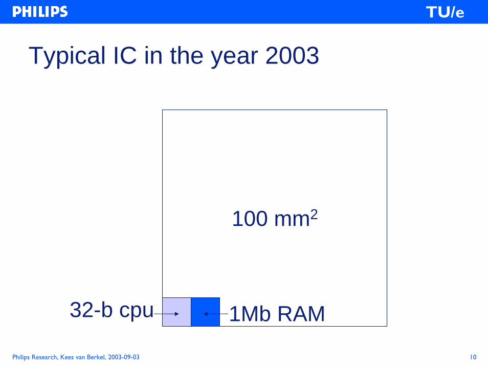
Typical IC in the year 2003
100 mm2
32-b cpu 1Mb RAM

Philips Research, Kees van Berkel, 2003-09-03 11
TU/e
Vertical cut through circuit
Philips Research, Kees van Berkel, 2003-09-03 12
TU/e
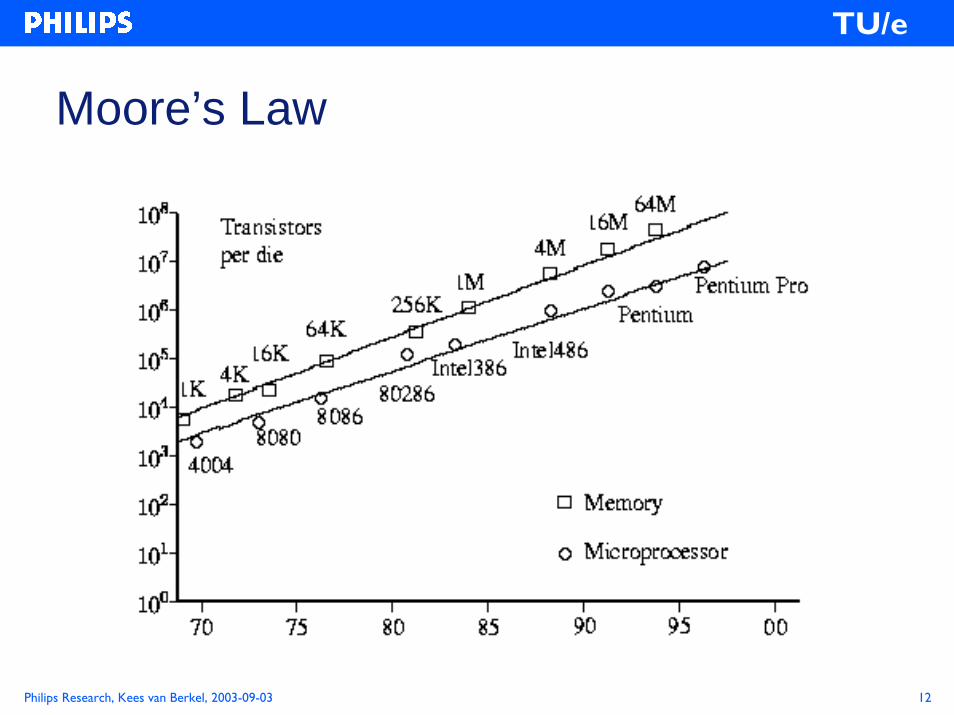
Moore’s Law
Philips Research, Kees van Berkel, 2003-09-03 13
TU/e
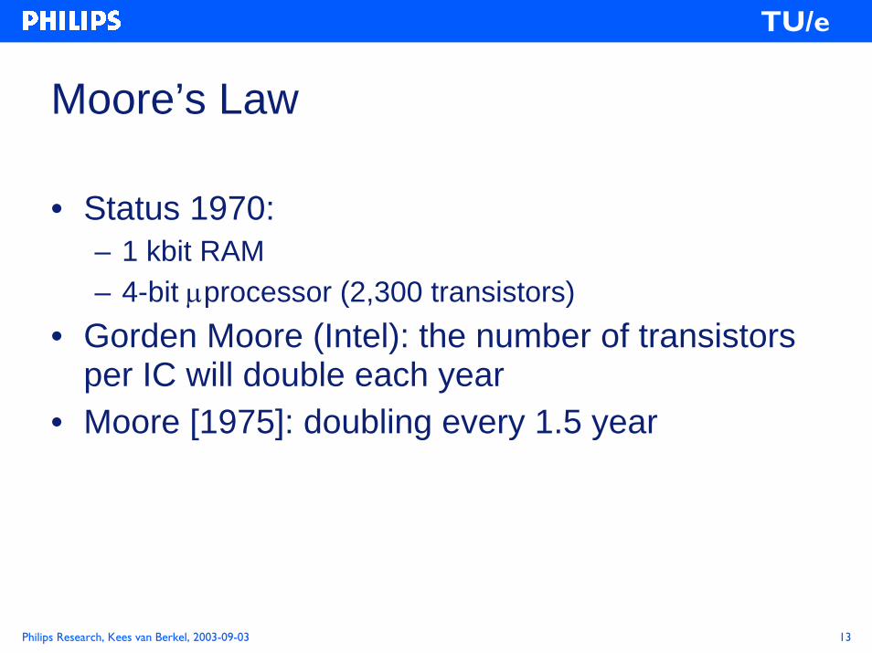
Moore’s Law
• Status 1970: – 1 kbit RAM– 4-bit µprocessor (2,300 transistors)
• Gorden Moore (Intel): the number of transistors per IC will double each year
• Moore [1975]: doubling every 1.5 year

Philips Research, Kees van Berkel, 2003-09-03 14
TU/e
Rule of two [Hu, 1993]
• Every 2 generations of IC technology (6 years)– device feature size 0.5 x– chip size 2 x– clock frequency 2 x– number of i/o pins 2 x– DRAM capacity 16 x– logic-gate density 4 x
Philips Research, Kees van Berkel, 2003-09-03 15
TU/e
ITRS roadmap
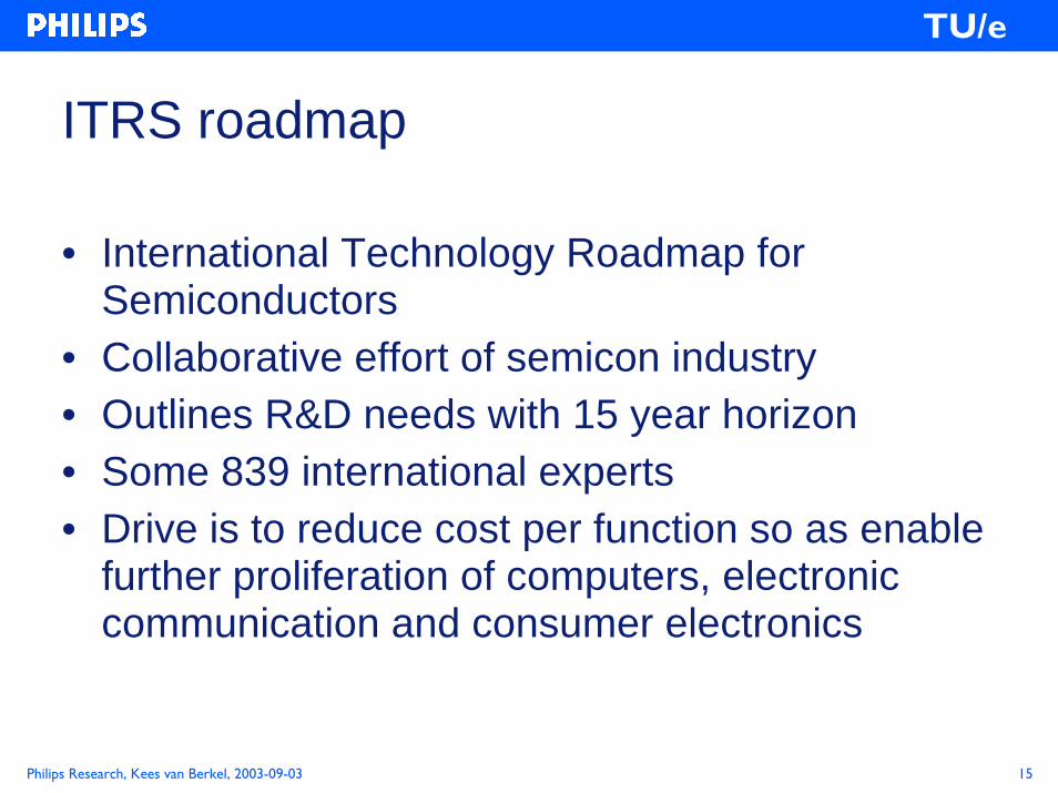
• International Technology Roadmap for Semiconductors
• Collaborative effort of semicon industry• Outlines R&D needs with 15 year horizon• Some 839 international experts• Drive is to reduce cost per function so as enable
further proliferation of computers, electronic communication and consumer electronics
Philips Research, Kees van Berkel, 2003-09-03 16
TU/e
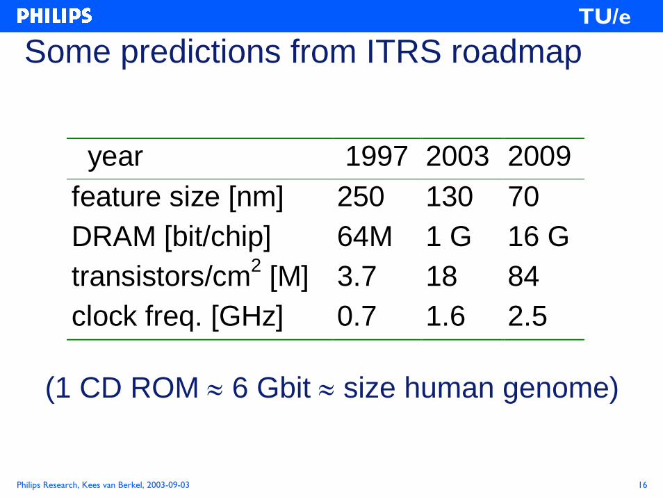
Some predictions from ITRS roadmap
year 1997 2003 2009feature size [nm] 250 130 70 DRAM [bit/chip] 64M 1 G 16 Gtransistors/cm2 [M] 3.7 18 84 clock freq. [GHz] 0.7 1.6 2.5
(1 CD ROM ≈ 6 Gbit ≈ size human genome)
Philips Research, Kees van Berkel, 2003-09-03 17
TU/e
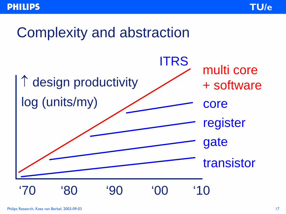
Complexity and abstraction
↑ design productivitylog (units/my)
ITRSmulti core + softwarecoreregistergate
transistor
‘70 ‘80 ‘90 ‘00 ‘10

Philips Research, Kees van Berkel, 2003-09-03 18
TU/e
VLSI programming of asynchronouscircuits
behavior,
area, time, energy,
test coverage
Tangram program
expander
Handshake circuit
Asynchronous circuit(netlist of gates)
compilersimulator
feedback
Philips Research, Kees van Berkel, 2003-09-03 19
TU/e
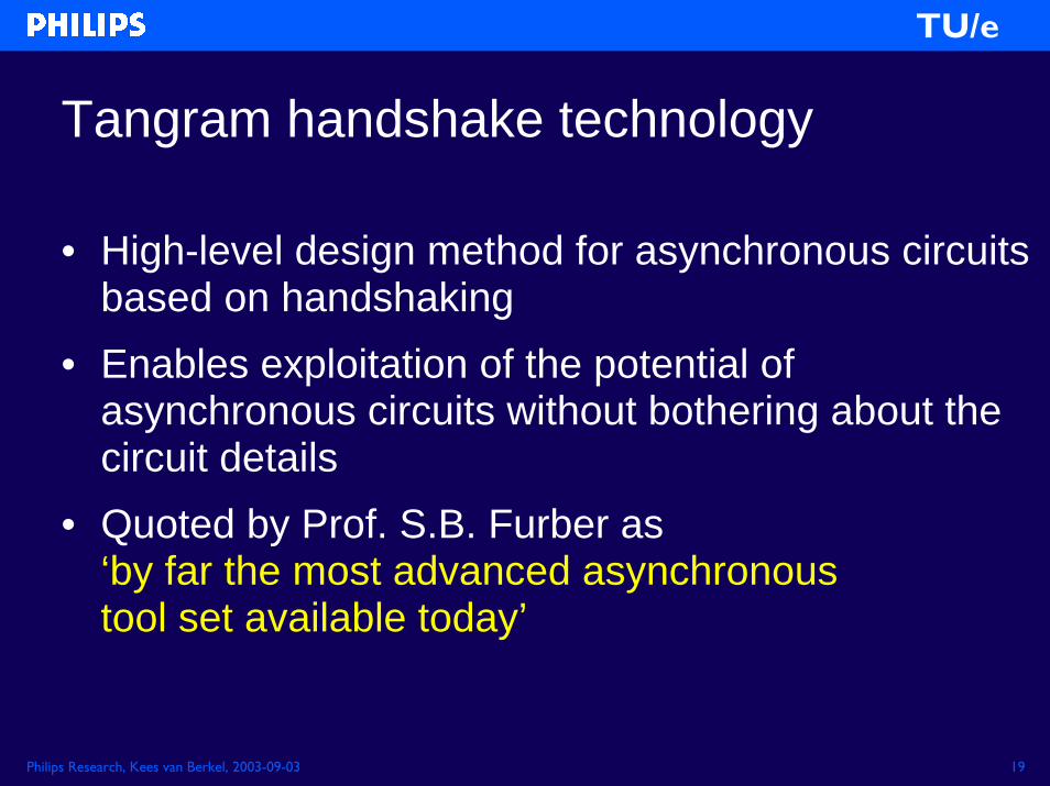
Tangram handshake technology
• High-level design method for asynchronous circuits based on handshaking
• Enables exploitation of the potential of asynchronous circuits without bothering about the circuit details
• Quoted by Prof. S.B. Furber as ‘by far the most advanced asynchronous tool set available today’

Philips Research, Kees van Berkel, 2003-09-03 20
TU/e
Tangram handshake technology
• Design technology for clockless digital ICs• Local handshake instead of global clock• Handshake between active and passive partner• Communication is by means of alternating
request (from active to passive) and acknowledge (from passive to active) signals
PassiveActive

Philips Research, Kees van Berkel, 2003-09-03 21
TU/e
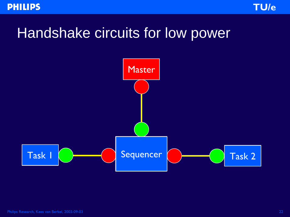
Handshake circuits
Sequencer
Master
Task 1 Task 2
Philips Research, Kees van Berkel, 2003-09-03 22
TU/e
Handshake circuits for low power
Sequencer
Master
Task 1 Task 2
Master
Sequencer
Master
SequencerTask 1Task 1 Sequencer Task 2SequencerSequencer Task 2
Master
Sequencer

Philips Research, Kees van Berkel, 2003-09-03 23
TU/e
Low power
Tangram 80c51Clocked 80c51

Philips Research, Kees van Berkel, 2003-09-03 24
TU/e
Low current peaks
Clocked 80c51 Tangram 80c51
Philips Research, Kees van Berkel, 2003-09-03 25
TU/e
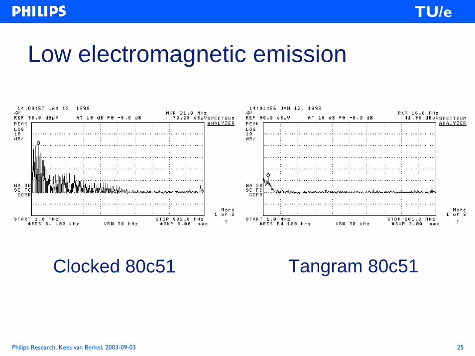
Low electromagnetic emission
Clocked 80c51 Tangram 80c51
Philips Research, Kees van Berkel, 2003-09-03 26
TU/e
Time for a break

Philips Research, Kees van Berkel, 2003-09-03 27
TU/e
Some common acronyms
• IC: Integrated Circuit [1960s]• LSI: Large Scale Integration [1970s]• VLSI: Very Large Scale Integration [1980s]• ULSI: Ultra Large Scale Integration [1990s]
(Proposed and rejected)
• Transistor: Tran(sfer) (re)sistorTransfers current across a resistor
Philips Research, Kees van Berkel, 2003-09-03 28
TU/e
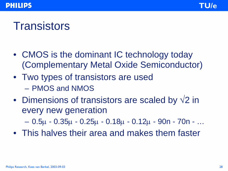
Transistors
• CMOS is the dominant IC technology today (Complementary Metal Oxide Semiconductor)
• Two types of transistors are used– PMOS and NMOS
• Dimensions of transistors are scaled by √2 in every new generation– 0.5µ - 0.35µ - 0.25µ - 0.18µ - 0.12µ - 90n - 70n - …
• This halves their area and makes them faster
Philips Research, Kees van Berkel, 2003-09-03 29
TU/e
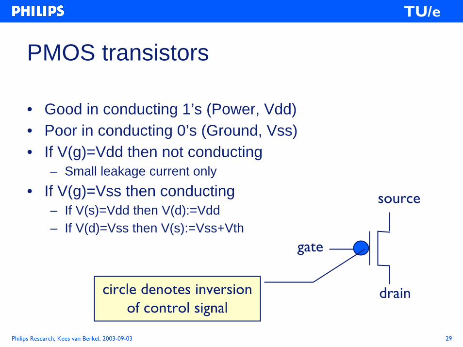
PMOS transistors
• Good in conducting 1’s (Power, Vdd)• Poor in conducting 0’s (Ground, Vss)• If V(g)=Vdd then not conducting
– Small leakage current only• If V(g)=Vss then conducting
– If V(s)=Vdd then V(d):=Vdd– If V(d)=Vss then V(s):=Vss+Vth
gate
source
draincircle denotes inversion of control signal
Philips Research, Kees van Berkel, 2003-09-03 30
TU/e
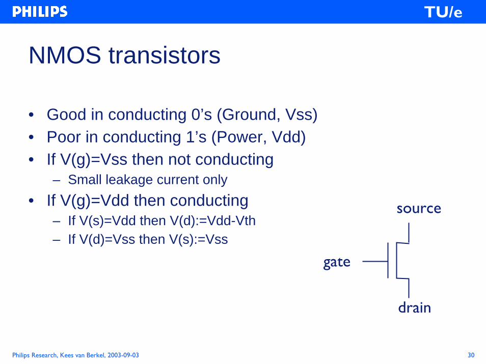
NMOS transistors
• Good in conducting 0’s (Ground, Vss) • Poor in conducting 1’s (Power, Vdd)• If V(g)=Vss then not conducting
– Small leakage current only• If V(g)=Vdd then conducting
– If V(s)=Vdd then V(d):=Vdd-Vth– If V(d)=Vss then V(s):=Vss
source
gate
drain

Philips Research, Kees van Berkel, 2003-09-03 31
TU/e
CMOS circuits• Pull-up stack consisting of only P-mosts• Pull-down stack consisting of only N-mosts• Only inverting gates can thus be formed
Vdd
Vss
+
–V
Pull-up
Pull-down
P
N

Philips Research, Kees van Berkel, 2003-09-03 32
TU/e
VLSI basics
Vdd (power)
Vss (ground)
C
+
–V
Charge Q
wire
gate

Philips Research, Kees van Berkel, 2003-09-03 33
TU/e
Transitions on a wireoutput z
input a
Vdd (power)
Vss (ground)
gate delay gate delay
input a output z
time →
Philips Research, Kees van Berkel, 2003-09-03 34
TU/e
VLSI basics
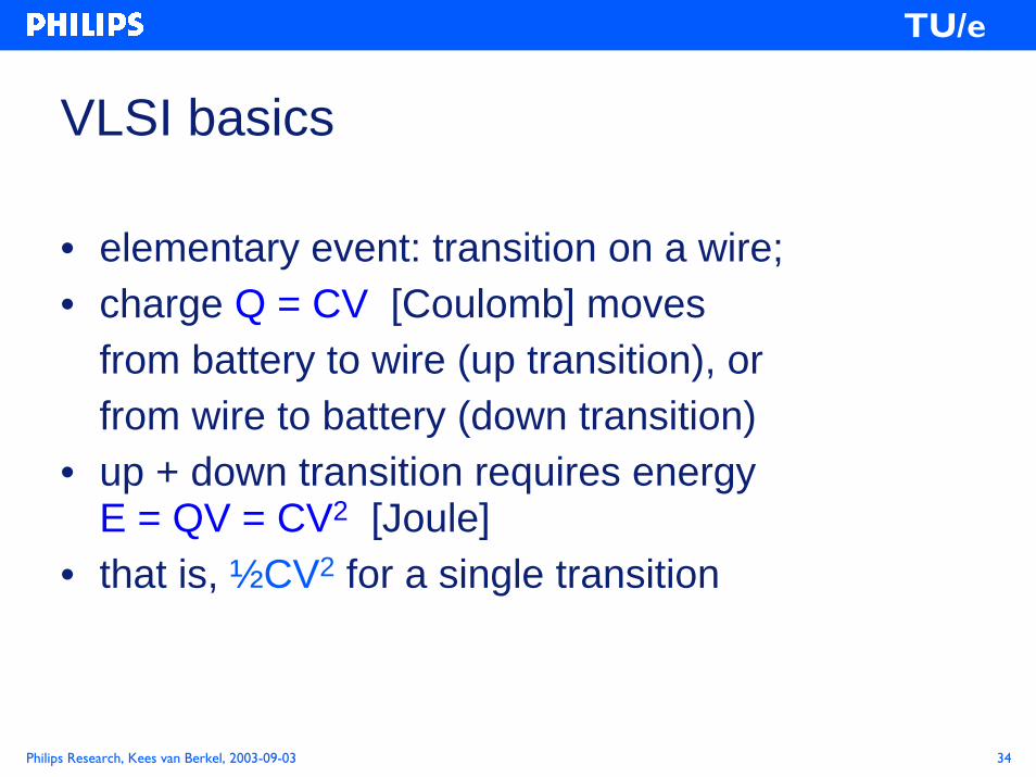
• elementary event: transition on a wire;• charge Q = CV [Coulomb] moves
from battery to wire (up transition), orfrom wire to battery (down transition)
• up + down transition requires energyE = QV = CV2 [Joule]
• that is, ½CV2 for a single transition
Philips Research, Kees van Berkel, 2003-09-03 35
TU/e
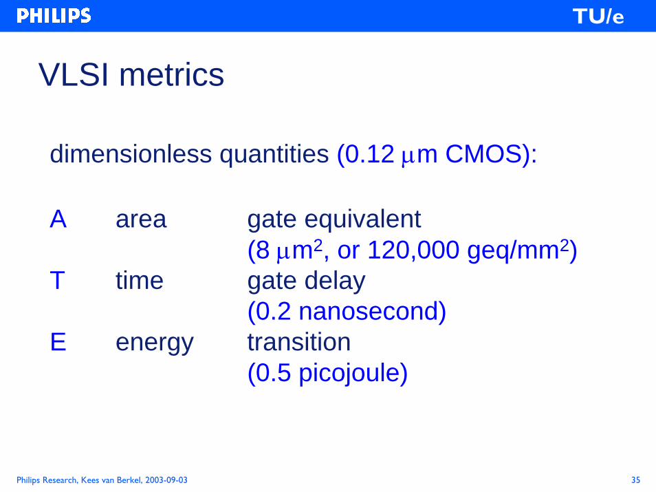
VLSI metrics
dimensionless quantities (0.12 µm CMOS):
A area gate equivalent(8 µm2, or 120,000 geq/mm2)
T time gate delay(0.2 nanosecond)
E energy transition(0.5 picojoule)
Philips Research, Kees van Berkel, 2003-09-03 36
TU/e
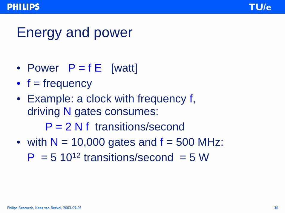
Energy and power
• Power P = f E [watt]• f = frequency• Example: a clock with frequency f,
driving N gates consumes:P = 2 N f transitions/second
• with N = 10,000 gates and f = 500 MHz:P = 5 1012 transitions/second = 5 W
Philips Research, Kees van Berkel, 2003-09-03 37
TU/e
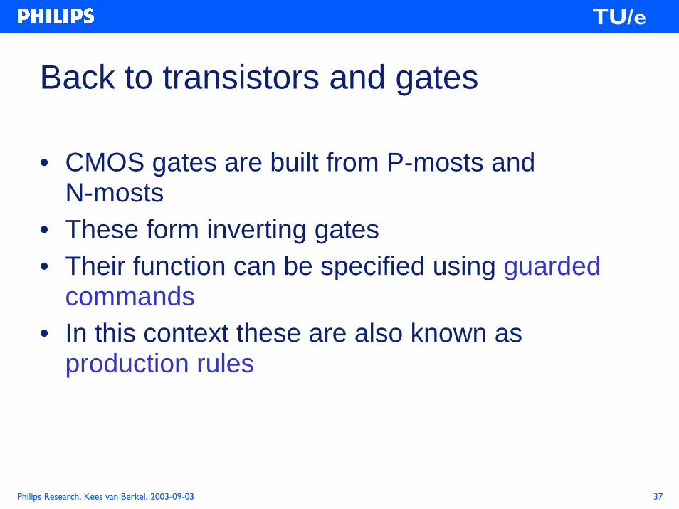
Back to transistors and gates
• CMOS gates are built from P-mosts and N-mosts
• These form inverting gates• Their function can be specified using guarded
commands• In this context these are also known as
production rules

Philips Research, Kees van Berkel, 2003-09-03 38
TU/e
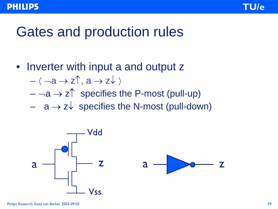
Gates and production rules
• A gate with inputs a, b, … and output z• Behavior (function) of a gate is specified by pair
of so-called production rules:⟨ F → z↑, G → z↓ ⟩
• z↑ is a shorthand for z := true • z↓ is a shorthand for z := false• F and G are so-called guards
(boolean expressions on the inputs of the gate)
Philips Research, Kees van Berkel, 2003-09-03 39
TU/e
Gates and production rules
• Inverter with input a and output z– ⟨ ¬a → z↑, a → z↓ ⟩– ¬a → z↑ specifies the P-most (pull-up)– a → z↓ specifies the N-most (pull-down)
zaz
Vss
Vdd
a

Philips Research, Kees van Berkel, 2003-09-03 40
TU/e
Gates and production rules
⟨ F → z↑, G → z↓ ⟩• Guards must be mutually exclusive, i.e.
¬F ∨ ¬G must hold at any time• This is to formalize the restriction to prevent
short-circuit behavior• “must hold at any time” does not necessarily
require that F⇒ ¬G or G⇒ ¬F • It may also impose a restriction on the
environment of the gate
Philips Research, Kees van Berkel, 2003-09-03 41
TU/e
Gates and production rules
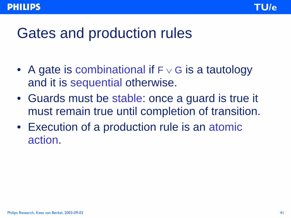
• A gate is combinational if F ∨ G is a tautology and it is sequential otherwise.
• Guards must be stable: once a guard is true it must remain true until completion of transition.
• Execution of a production rule is an atomic action.

Philips Research, Kees van Berkel, 2003-09-03 42
TU/e
Boolean functions and transistors
• Transistors can be put in series– Conducting only if all conducting– This implements an AND function
• Transistors can be put in parallel– Conducting if either is conducting – This implements an OR function
• Networks can build AND/OR functions
Philips Research, Kees van Berkel, 2003-09-03 43
TU/e
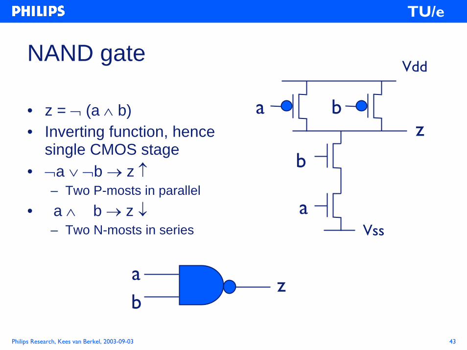
NAND gateVdd
• z = ¬ (a ∧ b)• Inverting function, hence
single CMOS stage • ¬a ∨ ¬b → z ↑
– Two P-mosts in parallel• a ∧ b → z ↓
– Two N-mosts in series Vss
a b
a
b
z
ab
z

Philips Research, Kees van Berkel, 2003-09-03 44
TU/e
AND gateVdd
• z = a ∧ b– a ∧ b → z ↑– ¬a ∨ ¬b → z ↓
• Non-inverting function, hence two CMOS stages
• First stage: NAND-gate– ¬a ∨ ¬b → y ↑– a ∧ b → y ↓
• Second stage: Inverter – ¬y → z ↑– y → z ↓
Vss
a b
a
bz
y
ab
z

Philips Research, Kees van Berkel, 2003-09-03 45
TU/e
Combinational CMOS gates
• Guards of production rules are complementary• This is reflected in the transistor stacksExercise• Draw transistor diagrams of
– Z = ¬(A ∨ (B ∧C ))– Z = (A≡B)
• What is their delay in terms of CMOS inversions ?• What is their cost (area) in # transistors ?
Philips Research, Kees van Berkel, 2003-09-03 46
TU/e
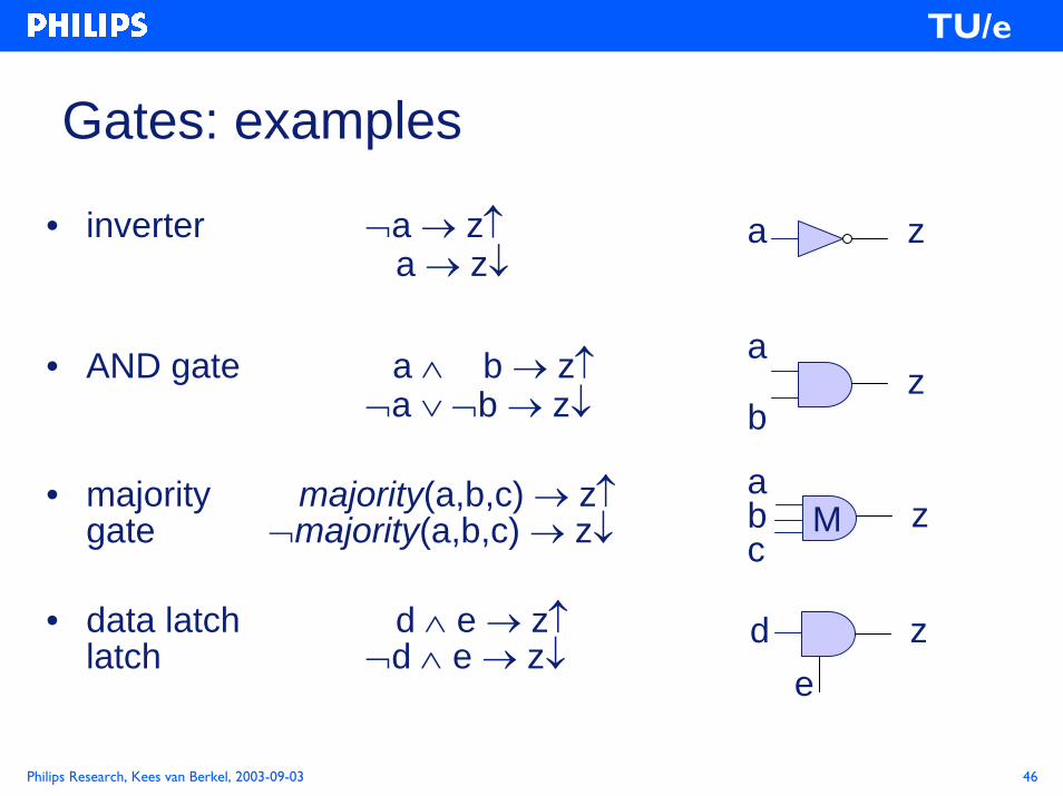
Gates: examples
• inverter ¬a → z↑a → z↓
• AND gate a ∧ b → z↑¬a ∨ ¬b → z↓
• majority majority(a,b,c) → z↑gate ¬majority(a,b,c) → z↓
• data latch d ∧ e → z↑latch ¬
a z
a
bz
de
z
Ma b c
z
d ∧ e → z↓
Philips Research, Kees van Berkel, 2003-09-03 47
TU/e
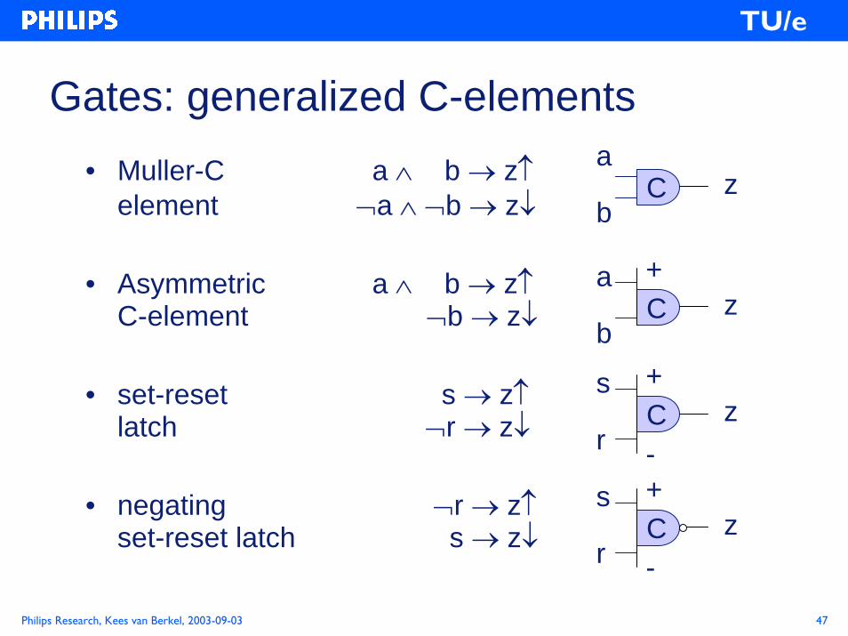
Gates: generalized C-elements• Muller-C a ∧ b → z↑
element ¬a ∧ ¬b → z↓
• Asymmetric a ∧ b → z↑C-element ¬b → z↓
• set-reset s → z↑latch ¬r → z↓
• negating ¬r → z↑set-reset latch s → z↓
Ca
bz
Ca
bz
+
Cs
rz
+
-
Cs
rz
+
-

Philips Research, Kees van Berkel, 2003-09-03 48
TU/e
Realization of a Majority gate:
pull-up paths
pull-down paths
(a ∧ b) ∨ (b ∧ c) ∨ (c ∧ a) → z↑(¬a ∧¬b) ∨ (¬b ∧¬c) ∨ (¬c ∧¬a) → z↓

Philips Research, Kees van Berkel, 2003-09-03 49
TU/e
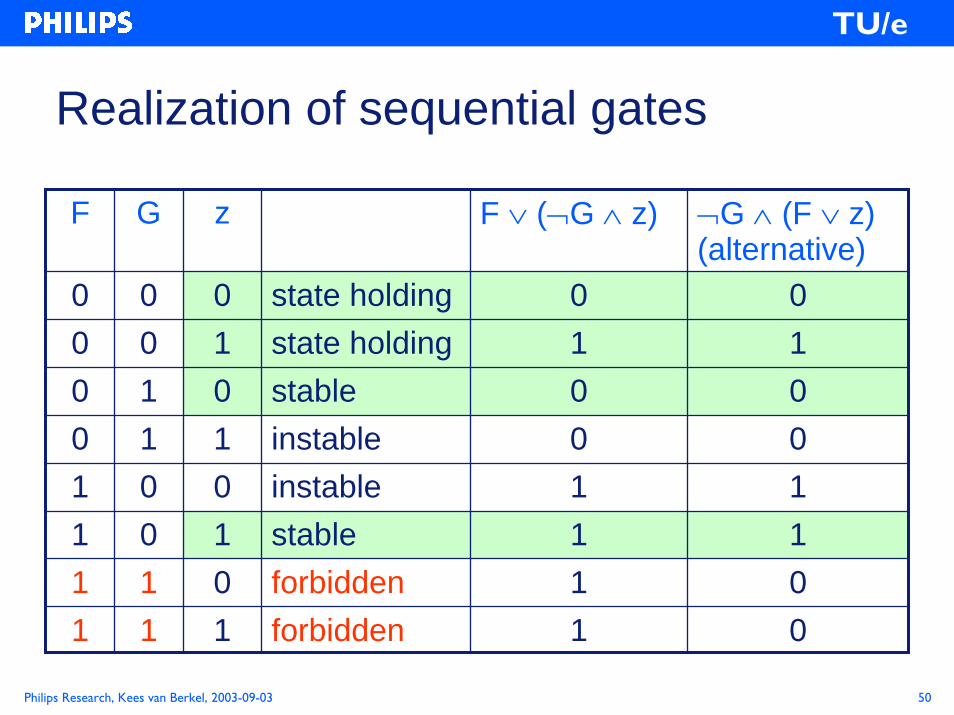
Realization of sequential gates
• Transform ⟨ F → z↑, G → z↓⟩into a combinational gate with feedback, by weakening the guards: ⟨ F ∨ (¬G ∧ z) → z↑, G ∨ (¬F∧ ¬z) → z↓ ⟩
• and by using that ¬(F∧G) holds invariantly:⟨ F ∨ (¬G ∧ z) → z↑ , ¬(F ∨ (¬G ∧ z)) → z↓ ⟩
• Hence, any sequential gate can be realized by combinational gate z = F ∨ (¬G ∧ z).
ab
z
feedback
forkcombinational gate
Philips Research, Kees van Berkel, 2003-09-03 50
TU/e
Realization of sequential gates
F G z F ∨ (¬G ∧ z) ¬G ∧ (F ∨ z)(alternative)
0 0 0 state holding 0 00 0 1 state holding 1 10 1 0 stable 0 00 1 1 instable 0 01 0 0 instable 1 11 0 1 stable 1 11 1 0 forbidden 1 01 1 1 forbidden 1 0

Philips Research, Kees van Berkel, 2003-09-03 51
TU/e
Realization of a Muller-C elementProduction rules: ⟨ a ∧ b → z↑, ¬a ∧ ¬b → z↓⟩
z = F ∨ (¬G ∧ z)= a ∧ b ∨ (¬(¬a ∧ ¬b ) ∧ z) = majority(a,b,z)
a
a
b
a
a
b
b
b
z
zz
vss
vdd

Philips Research, Kees van Berkel, 2003-09-03 52
TU/e
Realization of Muller-C elements
a
a
b
a
a
b
b
b
z
zz
vss
vdd vdda z
a z
b
b
vss
a ∧ b ∧ c → z↑¬a ∧ ¬b ∧ ¬c → z↓
z cz
z c
a ∧ b → z↑¬a ∧ ¬b → z↓
Philips Research, Kees van Berkel, 2003-09-03 53
TU/e
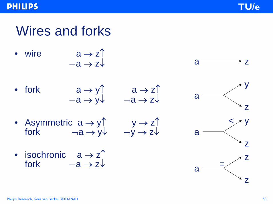
Wires and forks• wire a → z↑
¬a → z↓
• fork a → y↑ a → z↑¬a → y↓ ¬a → z↓
• Asymmetric a → y↑ y → z↑fork ¬a → y↓ ¬y → z↓
• isochronic a → z↑fork ¬a
a z
ay
zy<
az
az
z
=→ z↓

Philips Research, Kees van Berkel, 2003-09-03 54
TU/e
Next week: lecture 2
Outline:• Handshake signaling• Handshake behaviors; program notation • Handshake components • … and their realization as networks of gates • Handshake circuits
