introduction to - r.m.k. college of engineering and...
TRANSCRIPT


Introduction
to
Microcontrollers
8051 Microcontroller 2

Microprocessor vs. Microcontroller
Microprocessor
• CPU is stand-alone, RAM, ROM, I/O, timer are separate
• Designer can decide on the amount of ROM, RAM and I/O ports.
• Expansive
• Versatility
• General-purpose
Microcontroller
• CPU, RAM, ROM, I/O and timer are all on a single chip
• Fix amount of on-chip ROM, RAM, I/O ports
• For applications in which cost, power and space are critical
• Not Expansive
• Single-purpose
8051 Microcontroller 3

8051 CPU Operation
1. Features
2. Pin Diagram
3. Block Diagram
8051 Microcontroller 4

8051 Microcontroller
• Intel introduced 8051, referred as MCS- 51, in1981.
• The 8051 is an 8-bit processor– The CPU can work on only 8 bits of data at a time
• The 8051 became widely popular after allowingother manufactures to make and market anyflavor of the 8051.
8051 Microcontroller 5

8051 Family
• The 8051 is a subset of the 8052
• The 8031 is a ROM-less 8051
– Add external ROM to it
– You lose two ports, and leave only 2 ports for I/O operations
8051 Microcontroller 6

8051 Features
• 64KB Program Memory address space
• 64KB Data Memory address space
• 4K bytes of on-chip Program Memory
• 128 bytes of on-chip Data RAM
• 32 bidirectional and individually addressable I/0 lines
• Two 16-bit timer/counters
• Full duplex UART
• 6-source/5-vector interrupt structure with two priority levels
• On-chip clock oscillator
8051 Microcontroller 7

Pin Description of the 8051
• 8051 family members (e.g., 8751, 89C51, 89C52,DS89C4x0)
– Have 40 pins dedicated for various functions such as I/O, RD,WR, address, data, and interrupts.
– Come in different packages, such as• DIP(dual in-line package),
• QFP(quad flat package), and• LLC(leadless chip carrier)
• Some companies provide a 20-pin version of the 8051with a reduced number of I/O ports for less demandingapplications
8051 Microcontroller 8

Pin Diagram of the 8051
8051 Microcontroller 9

XTAL1 and XTAL2
• The 8051 has an on-chip oscillator but requires an external clock to run it
– A quartz crystal oscillator is connected to inputs XTAL1 (pin19) and XTAL2 (pin18)
– The quartz crystal oscillator also needs two capacitors of 30 pF value
8051 Microcontroller 10

XTAL1 and XTAL2 …..
• If you use a frequency source other than a crystal oscillator, such as a TTL oscillator:
– It will be connected to XTAL1
– XTAL2 is left unconnected
8051 Microcontroller 11

XTAL1 and XTAL2 …..
• The speed of 8051 refers to the maximum oscillatorfrequency connected to XTAL.
• We can observe the frequency on the XTAL2 pin usingthe oscilloscope.
8051 Microcontroller 12

RST
• RESET pin is an input and is active high (normally low)
• Upon applying a high pulse to this pin, the microcontroller willreset and terminate all activities
• This is often referred to as a power-on reset
• Activating a power-on reset will cause all values in the registers tobe lost
8051 Microcontroller 13

RST
• In order for the RESET input to be effective, it must have a minimum duration of 2 machine cycles.
• In other words, the high pulse must be high for aminimum of 2 machine cycles before it is allowed to golow.
8051 Microcontroller 14

EA’
• EA’, “external access’’, is an input pin andmust be connected to Vcc or GND
• The 8051 family members all come with on-chip ROM to store programs and also havean external code and data memory.
• Normally EA pin is connected to Vcc
• EA pin must be connected to GND toindicate that the code or data is storedexternally.
8051 Microcontroller 15
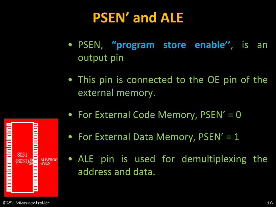
PSEN’ and ALE
• PSEN, “program store enable’’, is anoutput pin
• This pin is connected to the OE pin of theexternal memory.
• For External Code Memory, PSEN’ = 0
• For External Data Memory, PSEN’ = 1
• ALE pin is used for demultiplexing theaddress and data.
8051 Microcontroller 16

I/O Port Pins
• The four 8-bit I/O ports P0, P1, P2and P3 each uses 8 pins.
• All the ports upon RESET areconfigured as output, ready to beused as input ports by the externaldevice.
8051 Microcontroller 17

Port 0
• Port 0 is also designated as AD0-AD7.
• When connecting an 8051 to an externalmemory, port 0 provides both address anddata.
• The 8051 multiplexes address and datathrough port 0 to save pins.
• ALE indicates if P0 has address or data.
– When ALE=0, it provides data D0-D7
– When ALE=1, it has address A0-A7
8051 Microcontroller 18
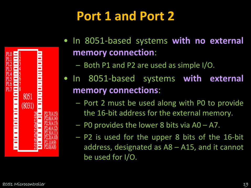
Port 1 and Port 2
• In 8051-based systems with no externalmemory connection:
– Both P1 and P2 are used as simple I/O.
• In 8051-based systems with externalmemory connections:
– Port 2 must be used along with P0 to providethe 16-bit address for the external memory.
– P0 provides the lower 8 bits via A0 – A7.
– P2 is used for the upper 8 bits of the 16-bitaddress, designated as A8 – A15, and it cannotbe used for I/O.
8051 Microcontroller 19
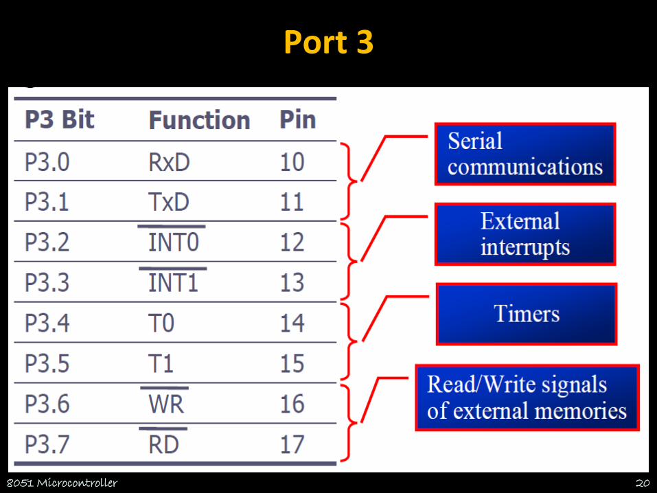
Port 3
• Port 3 can be used as input or output.
• Port 3 has the additional function ofproviding some extremely importantsignals
8051 Microcontroller 20

Pin Description Summary
8051 Microcontroller 21
PIN TYPE NAME AND FUNCTION
Vss I Ground: 0 V reference.
Vcc I Power Supply: This is the power supply voltage for normal,idle, and power-down operation.
P0.0 - P0.7 I/O Port 0: Port 0 is an open-drain, bi-directional I/O port. Port0 is also the multiplexed low-order address and data busduring accesses to external program and data memory.
P1.0 - P1.7 I/O Port 1: Port I is an 8-bit bi-directional I/O port.
P2.0 - P2.7 I/O Port 2: Port 2 is an 8-bit bidirectional I/O. Port 2 emits thehigh order address byte during fetches from externalprogram memory and during accesses to external datamemory that use 16 bit addresses.
P3.0 - P3.7 I/O Port 3: Port 3 is an 8 bit bidirectional I/O port. Port 3 alsoserves special features as explained.

Pin Description Summary
8051 Microcontroller 22
PIN TYPE NAME AND FUNCTION
RST I Reset: A high on this pin for two machine cycles while theoscillator is running, resets the device.
ALE O Address Latch Enable: Output pulse for latching the low byteof the address during an access to external memory.
PSEN* O Program Store Enable: The read strobe to external programmemory. When executing code from the external programmemory, PSEN* is activated twice each machine cycle,except that two PSEN* activations are skipped duringeach access to external data memory.
EA*/VPP I External Access Enable/Programming Supply Voltage: EA*must be externally held low to enable the device to fetchcode from external program memory locations. If EA* Isheld high, the device executes from internal programmemory. This pin also receives the programming supplyvoltage Vpp during Flash programming. (applies for 89c5xMCU's)

Interrupt
Control
CPU
4K
ROM128 B
RAM
OSCBus
Control4 I/O Ports
Serial
Port
Timer 1
Timer 0
General Block Diagram of 8051
TXD RXDP0 P1 P2 P3

Detailed Block Diagram
8051 Microcontroller 24

8051
Memory Space
8051 Microcontroller 25

8051 Memory Structure
Exte
rnal
EXT INT128
SFR
Ex
tern
al
Program Memory Data Memory
64K 64K
EA = 0 EA = 1
4K
60K
8051 Microcontroller 26

Internal RAM Structure
Direct &Indirect
Addressing
DirectAddressing
OnlySFR [ Special Function Registers]
128 Byte Internal RAM
8051 Microcontroller 27
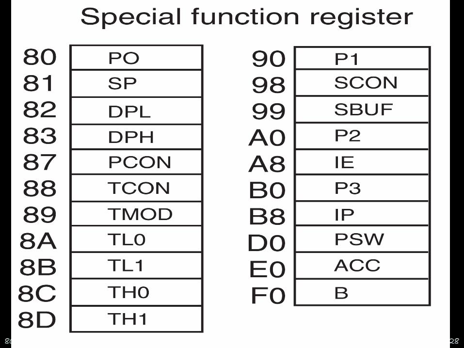
Special Function Registers [SFR]
8051 Microcontroller 28

Program Status Word [PSW]
8051 Microcontroller 29
C AC F0 RS1 RS0 OV F1 P
Register Bank Select
Carry
Auxiliary Carry
User Flag 0
Parity
User Flag 1
Overflow

8051 instructions that affects flag
8051 Microcontroller 30

128 Byte RAM
• There are 128 bytes of RAM in the 8051.
– Assigned addresses 00 to 7FH
• The 128 bytes are divided into 3 differentgroups as follows:
1. A total of 32 bytes from locations 00 to 1Fhex are set aside for register banks and thestack.
2. A total of 16 bytes from locations 20H to 2FHare set aside for bit-addressable read/writememory.
3. A total of 80 bytes from locations 30H to 7FHare used for read and write storage, calledscratch pad.
8051 Microcontroller 31
128 BYTE
INTERNAL RAM
Register Banks
Reg Bank 0
Reg Bank 1
Reg Bank 2
Reg Bank 3
BIT AddressableArea
General PurposeArea

8051 RAM with addresses
8051 Microcontroller 32

8051 Register Bank Structure
Bank 0
R0 R1 R2 R3 R4 R5 R6 R7Bank 3
R0 R1 R2 R3 R4 R5 R6 R7Bank 2
R0 R1 R2 R3 R4 R5 R6 R7Bank 1
R0 R1 R2 R3 R4 R5 R6 R7
8051 Microcontroller 33

8051 Register Banks with address
8051 Microcontroller 34

8051 Programming Model
8051 Microcontroller 35

8051 Stack
• The stack is a section of RAM used by the CPU to storeinformation temporarily.
– This information could be data or an address
• The register used to access the stack is called the SP(stack pointer) register
– The stack pointer in the 8051 is only 8 bit wide, which meansthat it can take value of 00 to FFH
– When the 8051 is powered up, the SP register contains value07
– RAM location 08 is the first location begin used for the stack bythe 8051
8051 Microcontroller 36
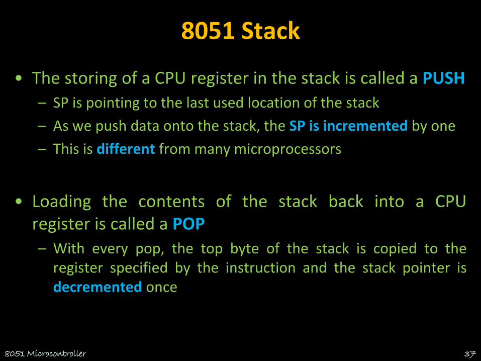
8051 Stack
• The storing of a CPU register in the stack is called a PUSH
– SP is pointing to the last used location of the stack
– As we push data onto the stack, the SP is incremented by one
– This is different from many microprocessors
• Loading the contents of the stack back into a CPUregister is called a POP
– With every pop, the top byte of the stack is copied to theregister specified by the instruction and the stack pointer isdecremented once
8051 Microcontroller 37

Bit Addressable & Byte Addressable
8051 Microcontroller 38

Single bit Instructions
8051 Microcontroller 39

Bit Addressable Programming
• Example: Find out to which by each of the following bits belongs. Give the address of the RAM byte in hex
(a) SETB 42H, (b) CLR 67H, (c) CLR 0FH (d) SETB 28H, (e) CLR 12, (f) SETB 05
8051 Microcontroller 40

8051 Peripheral Overview
1. Timers
2. Serial Port
3. Interrupts
8051 Microcontroller 41

8051
TIMERS8051 Microcontroller 42

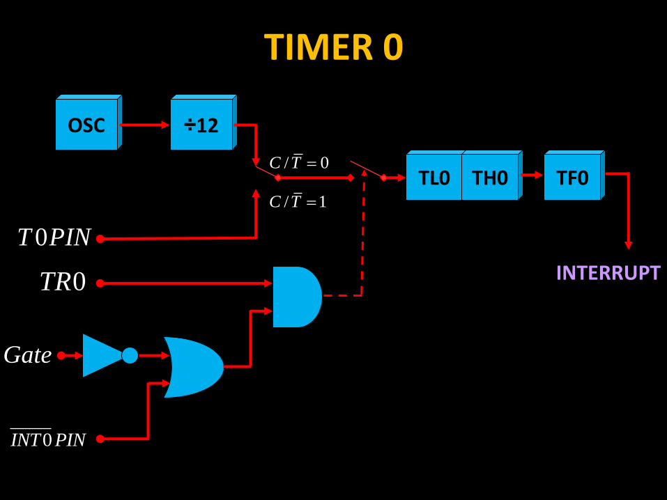
8051 Timer/Counter
8051 Microcontroller 43
OSC ÷12
TLx(8 Bit)
/ 0C T
/ 1C T
INT PIN
Gate
TR
T PIN
THx(8 Bit)
TFx(1 Bit)
INTERRUPT

TMOD Register
8051 Microcontroller 44
GATE:
When set, timer/counter x is enabled, if INTx pin is high
and TRx is set.
When cleared, timer/counter x is enabled, if TRx bit set.
C/T*:
When set, counter operation (input from Tx input pin).
When cleared, timer operation (input from internal clock).

TMOD Register
8051 Microcontroller 45
The TMOD byte is not bit addressable.

TCON Register
8051 Microcontroller 46

8051 Timer Modes
8051 Microcontroller 47
Timer 0
Mode 3
Mode 2
Mode 1
Mode 0
Mode 2
Mode 1
Mode 0
Timer 1
8051 TIMERS
OSC ÷12
TL0/ 0C T
/ 1C T
0INT PIN
Gate
0TR
0T PIN
TH0
INTERRUPT
TIMER 0
TF0

TL0(5 Bit)
INTERRUPT
TIMER 0 – Mode 0
OSC ÷12/ 0C T
/ 1C T
0INT PIN
Gate
0TR
0T PIN
TH0(8 Bit)
TF0
13 Bit Timer / Counter
Maximum Count = 1FFFh (0001111111111111)

TL0(8 Bit)
INTERRUPT
TIMER 0 – Mode 1
OSC ÷12/ 0C T
/ 1C T
0INT PIN
Gate
0TR
0T PIN
TH0(8 Bit)
TF0
16 Bit Timer / Counter
Maximum Count = FFFFh (1111111111111111)
TH0(8 Bit)
Reload
TIMER 0 – Mode 2
8 Bit Timer / Counter with AUTORELOAD
TL0(8 Bit)
OSC ÷12/ 0C T
/ 1C T
0INT PIN
Gate
0TR
0T PIN
TH0(8 Bit)
TF0 INTERRUPT
Maximum Count = FFh (11111111)

TL0(8 Bit)
INTERRUPT
TIMER 0 – Mode 3
OSC ÷12/ 0C T
/ 1C T
0INT PIN
Gate
0TR
0T PIN
TF0
Two - 8 Bit Timer / Counter
OSC ÷12
1TR
TH0(8 Bit)
INTERRUPTTF1

OSC ÷12
TL1/ 0C T
/ 1C T
Gate
TH1
INTERRUPT
TIMER 1
TF1
1INT PIN
1TR
1T PIN

TL1(5 Bit)
INTERRUPT
TIMER 1 – Mode 0
OSC ÷12/ 0C T
/ 1C T
Gate
TH1(8 Bit)
TF1
13 Bit Timer / Counter
Maximum Count = 1FFFh (0001111111111111)
1INT PIN
1TR
1T PIN

TL1(8 Bit)
INTERRUPT
TIMER 1 – Mode 1
OSC ÷12/ 0C T
/ 1C T
Gate
TH1(8 Bit)
TF1
16 Bit Timer / Counter
Maximum Count = FFFFh (1111111111111111)
1INT PIN
1TR
1T PIN

TH1(8 Bit)
Reload
TIMER 1 – Mode 2
8 Bit Timer / Counter with AUTORELOAD
TL1(8 Bit)
OSC ÷12/ 0C T
/ 1C T
Gate
TH1(8 Bit)
TF1 INTERRUPT
Maximum Count = FFh (11111111)
1INT PIN
1TR
1T PIN
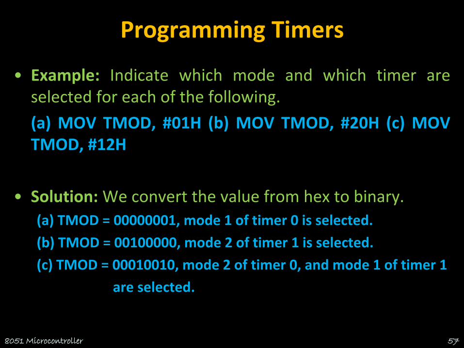
Programming Timers
• Example: Indicate which mode and which timer areselected for each of the following.
(a) MOV TMOD, #01H (b) MOV TMOD, #20H (c) MOVTMOD, #12H
• Solution: We convert the value from hex to binary.
(a) TMOD = 00000001, mode 1 of timer 0 is selected.
(b) TMOD = 00100000, mode 2 of timer 1 is selected.
(c) TMOD = 00010010, mode 2 of timer 0, and mode 1 of timer 1
are selected.
8051 Microcontroller 57

Programming Timers
• Find the timer’s clock frequency and its period forvarious 8051-based system, with the crystal frequency11.0592 MHz when C/T bit of TMOD is 0.
• Solution:
8051 Microcontroller 58
1/12 × 11.0529 MHz = 921.6 MHz;
T = 1/921.6 kHz = 1.085 us

8051
Serial
Port8051 Microcontroller 59

Basics of Serial Communication
• Computers transfer data in two ways:
– Parallel: Often 8 or more lines (wire conductors) are used totransfer data to a device that is only a few feet away.
– Serial: To transfer to a device located many meters away, theserial method is used. The data is sent one bit at a time.
8051 Microcontroller 60
Basics of Serial Communication
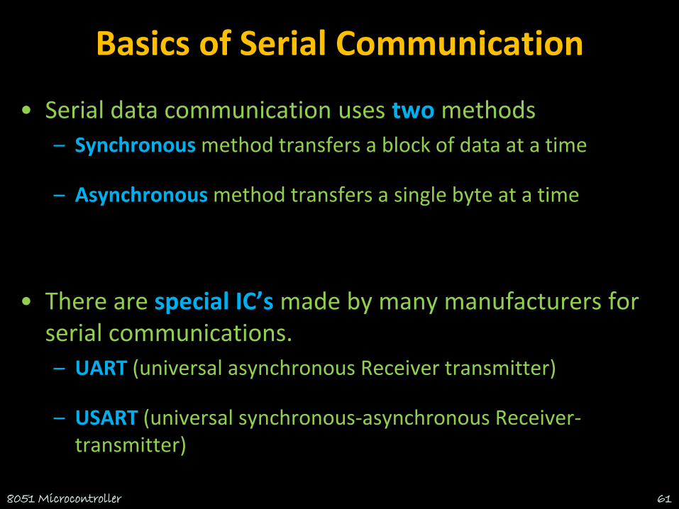
• Serial data communication uses two methods
– Synchronous method transfers a block of data at a time
– Asynchronous method transfers a single byte at a time
• There are special IC’s made by many manufacturers for serial communications.
– UART (universal asynchronous Receiver transmitter)
– USART (universal synchronous-asynchronous Receiver-transmitter)
8051 Microcontroller 61

Asynchronous – Start & Stop Bit
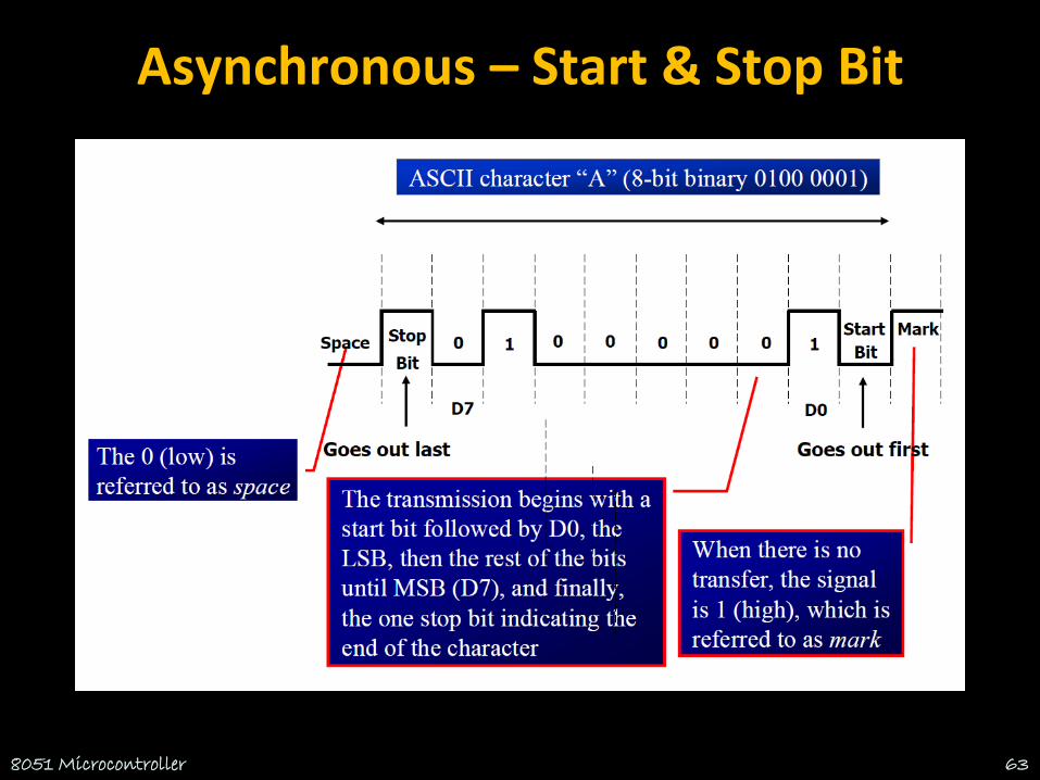
• Asynchronous serial data communication is widely used for character-oriented transmissions
– Each character is placed in between start and stop bits, this is called framing.
– Block-oriented data transfers use the synchronous method.
• The start bit is always one bit, but the stop bit can be one or two bits
• The start bit is always a 0 (low) and the stop bit(s) is 1 (high)
8051 Microcontroller 62
Asynchronous – Start & Stop Bit
8051 Microcontroller 63
Data Transfer Rate
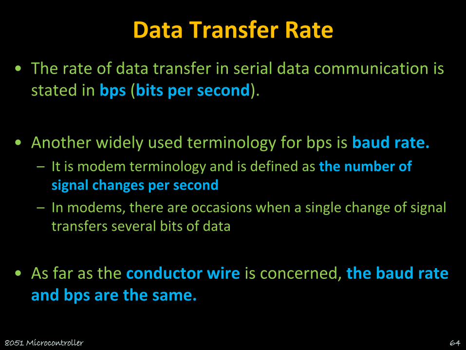
• The rate of data transfer in serial data communication is stated in bps (bits per second).
• Another widely used terminology for bps is baud rate.
– It is modem terminology and is defined as the number of signal changes per second
– In modems, there are occasions when a single change of signal transfers several bits of data
• As far as the conductor wire is concerned, the baud rate and bps are the same.
8051 Microcontroller 64

8051 Serial Port
• Synchronous and Asynchronous
• SCON Register is used to Control
• Data Transfer through TXd & RXd pins
• Some time - Clock through TXd Pin
• Four Modes of Operation:
8051 Microcontroller 65
Mode 0 :Synchronous Serial CommunicationMode 1 :8-Bit UART with Timer Data RateMode 2 :9-Bit UART with Set Data RateMode 3 :9-Bit UART with Timer Data Rate

Registers related to Serial Communication
1. SBUF Register
2. SCON Register
3. PCON Register
8051 Microcontroller 66
SBUF Register
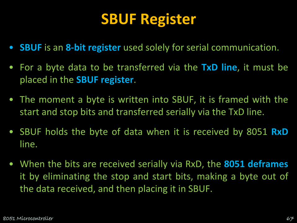
• SBUF is an 8-bit register used solely for serial communication.
• For a byte data to be transferred via the TxD line, it must beplaced in the SBUF register.
• The moment a byte is written into SBUF, it is framed with thestart and stop bits and transferred serially via the TxD line.
• SBUF holds the byte of data when it is received by 8051 RxDline.
• When the bits are received serially via RxD, the 8051 deframesit by eliminating the stop and start bits, making a byte out ofthe data received, and then placing it in SBUF.
8051 Microcontroller 67

SBUF Register
• Sample Program:
8051 Microcontroller 68

SCON Register
8051 Microcontroller 69
SM0 SM1 SM2 REN TB8 RB8 TI RI
Enable Multiprocessor
Communication Mode
Set to Enable
Serial Data
reception
9th Data Bit
Sent in Mode 2,3
9th Data Bit
Received in Mode 2,3
Set when Stop bit Txed
Set when a Cha-
ractor received
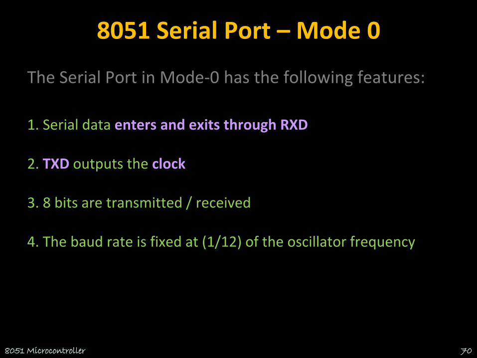
8051 Serial Port – Mode 0
The Serial Port in Mode-0 has the following features:
1. Serial data enters and exits through RXD
2. TXD outputs the clock
3. 8 bits are transmitted / received
4. The baud rate is fixed at (1/12) of the oscillator frequency
8051 Microcontroller 70

8051 Serial Port – Mode 1
The Serial Port in Mode-1 has the following features:
1. Serial data enters through RXD
2. Serial data exits through TXD
3. On receive, the stop bit goes into RB8 in SCON
4. 10 bits are transmitted / received
1. Start bit (0)
2. Data bits (8)
3. Stop Bit (1)
5. Baud rate is determined by the Timer 1 over flow rate.
8051 Microcontroller 71

8051 Serial Port – Mode 2
The Serial Port in Mode-2 has the following features:
1. Serial data enters through RXD
2. Serial data exits through TXD
3. 9th data bit (TB8) can be assign value 0 or 1
4. On receive, the 9th data bit goes into RB8 in SCON
5. 11 bits are transmitted / received
1.Start bit (0)
2.Data bits (9)
3.Stop Bit (1)
6. Baud rate is programmable
8051 Microcontroller 72

8051 Serial Port – Mode 3
The Serial Port in Mode-3 has the following features:
1. Serial data enters through RXD
2. Serial data exits through TXD
3. 9th data bit (TB8) can be assign value 0 or 1
4. On receive, the 9th data bit goes into RB8 in SCON
5. 11 bits are transmitted / received
1.Start bit (0)
2.Data bits (9)
3.Stop Bit (1)
6. Baud rate is determined by Timer 1 overflow rate.
8051 Microcontroller 73

Programming Serial Data Transmission1. TMOD register is loaded with the value 20H, indicating the use of timer
1 in mode 2 (8-bit auto-reload) to set baud rate.
2. The TH1 is loaded with one of the values to set baud rate for serial datatransfer.
3. The SCON register is loaded with the value 50H, indicating serial mode1, where an 8- bit data is framed with start and stop bits.
4. TR1 is set to 1 to start timer 1
5. TI is cleared by CLR TI instruction
6. The character byte to be transferred serially is written into SBUFregister.
7. The TI flag bit is monitored with the use of instruction JNB TI, xx to seeif the character has been transferred completely.
8. To transfer the next byte, go to step 5
8051 Microcontroller 74

Programming Serial Data Reception1. TMOD register is loaded with the value 20H, indicating the use of timer 1
in mode 2 (8-bit auto-reload) to set baud rate.
2. TH1 is loaded to set baud rate
3. The SCON register is loaded with the value 50H, indicating serial mode 1,where an 8- bit data is framed with start and stop bits.
4. TR1 is set to 1 to start timer 1
5. RI is cleared by CLR RI instruction
6. The RI flag bit is monitored with the use of instruction JNB RI, xx to see ifan entire character has been received yet
7. When RI is raised, SBUF has the byte, its contents are moved into a safeplace.
8. To receive the next character, go to step 5.
8051 Microcontroller 75

Doubling Baud Rate
• There are two ways to increase the baud rate of data transfer
1. By using a higher frequency crystal
2. By changing a bit in the PCON register
• PCON register is an 8-bit register.
8051 Microcontroller 76
•When 8051 is powered up, SMOD is zero
•We can set it to high by software and thereby double the baud rate.
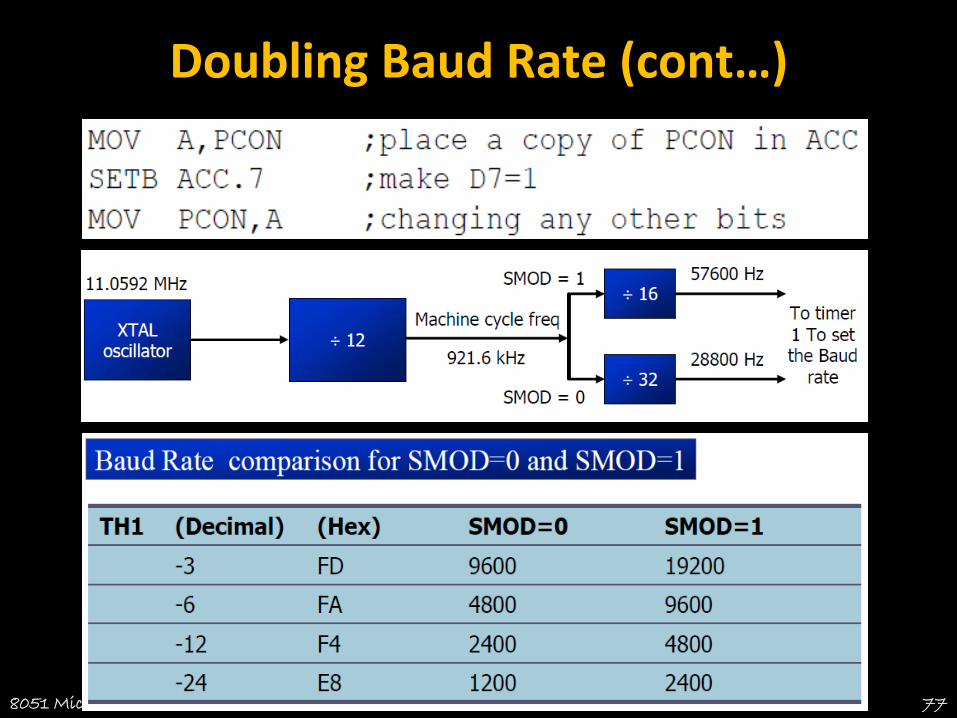
Doubling Baud Rate (cont…)
8051 Microcontroller 77

8051
Interrupts
8051 Microcontroller 78

INTERRUPTS
• An interrupt is an external or internal event thatinterrupts the microcontroller to inform it that a deviceneeds its service
• A single microcontroller can serve several devices by twoways:
1. Interrupt
2. Polling
8051 Microcontroller 79
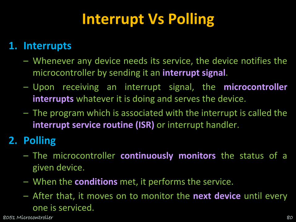
Interrupt Vs Polling
1. Interrupts
– Whenever any device needs its service, the device notifies themicrocontroller by sending it an interrupt signal.
– Upon receiving an interrupt signal, the microcontrollerinterrupts whatever it is doing and serves the device.
– The program which is associated with the interrupt is called theinterrupt service routine (ISR) or interrupt handler.
2. Polling
– The microcontroller continuously monitors the status of agiven device.
– When the conditions met, it performs the service.
– After that, it moves on to monitor the next device until everyone is serviced.
8051 Microcontroller 80

Interrupt Vs Polling
• The polling method is not efficient, since it wastes much ofthe microcontroller’s time by polling devices that do notneed service.
• The advantage of interrupts is that the microcontroller canserve many devices (not all at the same time).
• Each devices can get the attention of the microcontrollerbased on the assigned priority.
• For the polling method, it is not possible to assign prioritysince it checks all devices in a round-robin fashion.
• The microcontroller can also ignore (mask) a device requestfor service in Interrupt.
8051 Microcontroller 81

Steps in Executing an Interrupt1. It finishes the instruction it is executing and saves the address of
the next instruction (PC) on the stack.
2. It also saves the current status of all the interrupts internally (i.e:not on the stack).
3. It jumps to a fixed location in memory, called the interruptvector table, that holds the address of the ISR.
4. The microcontroller gets the address of the ISR from theinterrupt vector table and jumps to it.
5. It starts to execute the interrupt service subroutine until itreaches the last instruction of the subroutine which is RETI(return from interrupt).
6. Upon executing the RETI instruction, the microcontroller returnsto the place where it was interrupted.
8051 Microcontroller 82

Six Interrupts in 8051
Six interrupts are allocated as follows:
1. Reset – power-up reset.
2. Two interrupts are set aside for the timers.– one for timer 0 and one for timer 1
3. Two interrupts are set aside for hardware externalinterrupts.– P3.2 and P3.3 are for the external hardware interrupts INT0
(or EX1), and INT1 (or EX2)
4. Serial communication has a single interrupt thatbelongs to both receive and transfer.
8051 Microcontroller 83
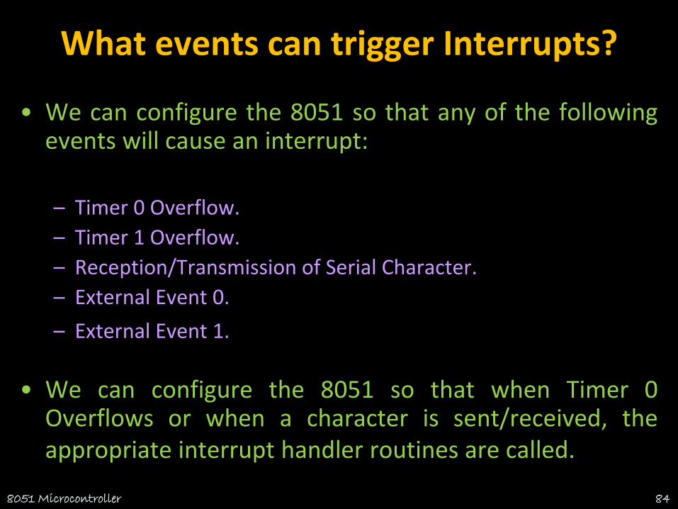
What events can trigger Interrupts?
• We can configure the 8051 so that any of the followingevents will cause an interrupt:
– Timer 0 Overflow.
– Timer 1 Overflow.
– Reception/Transmission of Serial Character.
– External Event 0.
– External Event 1.
• We can configure the 8051 so that when Timer 0Overflows or when a character is sent/received, theappropriate interrupt handler routines are called.
8051 Microcontroller 84

8051 Interrupt Vectors
8051 Microcontroller 85
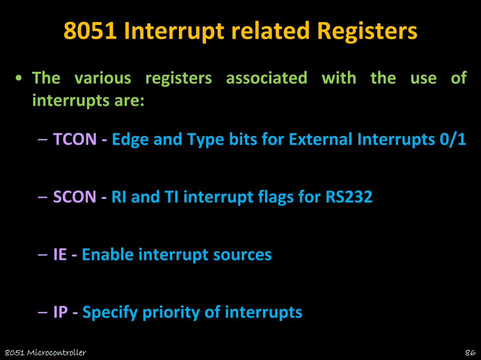
8051 Interrupt related Registers
• The various registers associated with the use ofinterrupts are:
– TCON - Edge and Type bits for External Interrupts 0/1
– SCON - RI and TI interrupt flags for RS232
– IE - Enable interrupt sources
– IP - Specify priority of interrupts
8051 Microcontroller 86
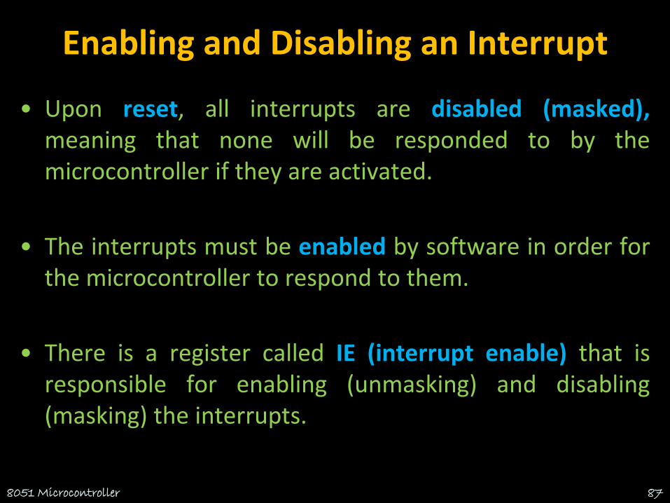
Enabling and Disabling an Interrupt
• Upon reset, all interrupts are disabled (masked),meaning that none will be responded to by themicrocontroller if they are activated.
• The interrupts must be enabled by software in order forthe microcontroller to respond to them.
• There is a register called IE (interrupt enable) that isresponsible for enabling (unmasking) and disabling(masking) the interrupts.
8051 Microcontroller 87

Interrupt Enable (IE) Register
8051 Microcontroller 88
• EA : Global enable/disable.
• --- : Reserved for additional interrupt hardware.
• ES : Enable Serial port interrupt.
• ET1 : Enable Timer 1 control bit.
• EX1 : Enable External 1 interrupt.
• ET0 : Enable Timer 0 control bit.
• EX0 : Enable External 0 interrupt.
MOV IE,#08h
or
SETB ET1
--

Enabling and Disabling an Interrupt• Example: Show the instructions to (a) enable the serial interrupt,
timer 0 interrupt, and external hardware interrupt 1 and (b)disable (mask) the timer 0 interrupt, then (c) show how to disableall the interrupts with a single instruction.
• Solution:
– (a) MOV IE,#10010110B ;enable serial, timer 0, EX1
• Another way to perform the same manipulation is:– SETB IE.7 ;EA=1, global enable
– SETB IE.4 ;enable serial interrupt
– SETB IE.1 ;enable Timer 0 interrupt– SETB IE.2 ;enable EX1
– (b) CLR IE.1 ;mask (disable) timer 0 interrupt only
– (c) CLR IE.7 ;disable all interrupts8051 Microcontroller 89

Interrupt Priority
• When the 8051 is powered up, the priorities are assigned accordingto the following.
• In reality, the priority scheme is nothing but an internal pollingsequence in which the 8051 polls the interrupts in the sequencelisted and responds accordingly.
8051 Microcontroller 90

Interrupt Priority
• We can alter the sequence of interrupt priority by assigning a higher priority to any one of the interrupts by programming a register called IP (interrupt priority).
• To give a higher priority to any of the interrupts, we make the corresponding bit in the IP register high.
8051 Microcontroller 91

Interrupt Priority (IP) Register
8051 Microcontroller 92
PS PT1 PX1 PT0 PX0Reserved
Serial Port
Timer 1 Pin
INT 1 Pin Timer 0 Pin
INT 0 Pin
Priority bit=1 assigns high priorityPriority bit=0 assigns low priority

Port 1 is denoted by P1.
P1.0 ~ P1.7
We use P1 as examples to show the operations on ports.
P1 as an output port (i.e., write CPU data to the external pin)
P1 as an input port (i.e., read pin data into CPU bus)
RMKCET/EEE/VAC/ES
Port 1(pins 1-8)

RMKCET/EEE/VAC/ES
8051 IC
D Q
Clk Q
Vcc
Load(L1)
Read latch
Read pin
Write to
latch
Internal
CPU bus
M
1
P1.X
pinP1.X
TB1
TB2
P0.x

Each pin of I/O ports
Internal CPU bus:communicate with CPU
A D latch store the value of this pin
D latch is controlled by “Write to latch”
Write to latch=1:write data into the D latch
2 Tri-state buffer:
TB1: controlled by “Read pin”
Read pin=1:really read the data present at the pin
TB2: controlled by “Read latch”
Read latch=1:read value from internal latch
A transistor M1 gate
Gate=0: open
Gate=1: close
RMKCET/EEE/VAC/ES

RMKCET/EEE/VAC/ES
Output Input
Tri-state control
(active high)
L H Low
Highimpedance
(open-circuit)HH
L H
RMKCET/EEE/VAC/ES
D Q
Clk Q
Vcc
Load(L1)
Read latch
Read pin
Write to
latch
Internal
CPU bus
M
1
P1.X
pinP1.X
8051 IC
2. output pin
is Vcc1. write a 1 to the pin1
0 output 1
TB1
TB2

RMKCET/EEE/VAC/ES
D Q
Clk Q
Vcc
Load(L1)
Read latch
Read pin
Write to
latch
Internal
CPU bus
M
1
P1.X
pinP1.X
8051 IC
2. output pin
is ground1. write a 0 to the pin0
1 output 0
TB1
TB2

Send data to Port 1:
MOV A,#55H
BACK: MOV P1,A
ACALL DELAY
CPL A
SJMP BACK
Let P1 toggle.
You can write to P1 directly.
RMKCET/EEE/VAC/ES

When reading ports, there are two possibilities:
Read the status of the input pin. (from external pin value)
MOV A, PX
JNB P2.1, TARGET ; jump if P2.1 is not set
JB P2.1, TARGET ; jump if P2.1 is set
Figures C-11, C-12
Read the internal latch of the output port.
ANL P1, A ; P1 ← P1 AND A
ORL P1, A ; P1 ← P1 OR A
INC P1 ; increase P1
Figure C-17
Table C-6 Read-Modify-Write Instruction (or Table 8-5)
See Section 8.3
RMKCET/EEE/VAC/ES

RMKCET/EEE/VAC/ES
D Q
Clk Q
Vcc
Load(L1)
Read latch
Read pin
Write to latch
Internal CPU
bus
M1
P1.X pin
P1.X
8051 IC
2. MOV A,P1
external pin=High1. write a 1 to the pin MOV
P1,#0FFH
1
0
3. Read pin=1 Read
latch=0 Write to latch=1
1
TB1
TB2

RMKCET/EEE/VAC/ES
D Q
Clk Q
Vcc
Load(L1)
Read latch
Read pin
Write to latch
Internal CPU
bus
M1
P1.X pin
P1.X
8051 IC
2. MOV A,P1
external pin=Low1. write a 1 to the pin
MOV P1,#0FFH
1
0
3. Read pin=1 Read
latch=0 Write to latch=1
0
TB1
TB2

In order to make P1 an input, the port must be programmed by writing 1
to all the bit.
MOV A,#0FFH ;A=11111111B
MOV P1,A ;make P1 an input port
BACK: MOV A,P1 ;get data from P0
MOV P2,A ;send data to P2
SJMP BACK
To be an input port, P0, P1, P2 and P3 have similar methods.
RMKCET/EEE/VAC/ES
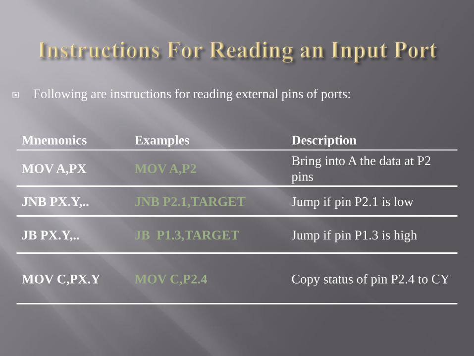
Mnemonics Examples Description
MOV A,PX MOV A,P2Bring into A the data at P2
pins
JNB PX.Y,.. JNB P2.1,TARGET Jump if pin P2.1 is low
JB PX.Y,.. JB P1.3,TARGET Jump if pin P1.3 is high
MOV C,PX.Y MOV C,P2.4 Copy status of pin P2.4 to CY
Following are instructions for reading external pins of ports:

Exclusive-or the Port 1:
MOV P1,#55H ;P1=01010101
ORL P1,#0F0H ;P1=11110101
1. The read latch activates TB2 and bring the data from the Q latch into
CPU.
Read P1.0=0
2. CPU performs an operation.
This data is ORed with bit 1 of register A. Get 1.
3. The latch is modified.
D latch of P1.0 has value 1.
4. The result is written to the external pin.
External pin (pin 1: P1.0) has value 1.
RMKCET/EEE/VAC/ES
RMKCET/EEE/VAC/ES
D Q
Clk Q
Vcc
Load(L1)
Read latch
Read pin
Write to latch
Internal CPU
bus
M1
P1.X pin
P1.X
8051 IC
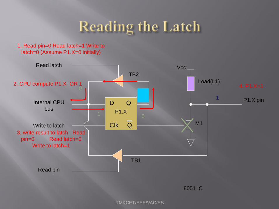
4. P1.X=12. CPU compute P1.X OR 1
0
0
1. Read pin=0 Read latch=1 Write to
latch=0 (Assume P1.X=0 initially)
1
TB1
TB2
3. write result to latch Read
pin=0 Read latch=0
Write to latch=1
1
0

Read-modify-write Instructions
Table C-6
This features combines 3 actions in a single instruction:
1. CPU reads the latch of the port
2. CPU perform the operation
3. Modifying the latch
4. Writing to the pin
Note that 8 pins of P1 work independently.
RMKCET/EEE/VAC/ES

Exclusive-or the Port 1:
MOV P1,#55H ;P1=01010101
AGAIN: XOR P1,#0FFH ;complement
ACALL DELAY
SJMP AGAIN
Note that the XOR of 55H and FFH gives AAH.
XOR of AAH and FFH gives 55H.
The instruction read the data in the latch (not from the pin).
The instruction result will put into the latch and the pin.
RMKCET/EEE/VAC/ES

RMKCET/EEE/VAC/ES
ExampleMnemonics
SETB P1.4SETB PX.Y
CLR P1.3CLR PX.Y
MOV P1.2,CMOV PX.Y,C
DJNZ P1,TARGETDJNZ PX,
TARGET
INC P1INC
CPL P1.2CPL
JBC P1.1,
TARGET
JBC PX.Y,
TARGET
XRL P1,AXRL
ORL P1,AORL
ANL P1,AANL
DEC P1DEC

How to write the data to a pin?
How to read the data from the pin?
Read the value present at the external pin.
Why we need to set the pin first?
Read the value come from the latch(not from the external
pin).
Why the instruction is called read-modify write?
RMKCET/EEE/VAC/ES

P1, P2, and P3 have internal pull-up resisters.
P1, P2, and P3 are not open drain.
P0 has no internal pull-up resistors and does not connects to
Vcc inside the 8051.
P0 is open drain.
Compare the figures of P1.X and P0.X.
However, for a programmer, it is the same to program P0, P1,
P2 and P3.
All the ports upon RESET are configured as output.
RMKCET/EEE/VAC/ES

RMKCET/EEE/VAC/ES
8051 IC
D Q
Clk Q
Read latch
Read pin
Write to
latch
Internal
CPU bus
M
1
P0.X
pinP1.X
TB1
TB2
P1.x
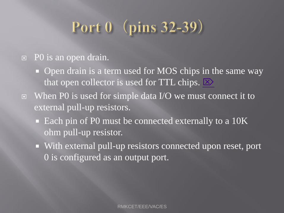
P0 is an open drain.
Open drain is a term used for MOS chips in the same way
that open collector is used for TTL chips.
When P0 is used for simple data I/O we must connect it to
external pull-up resistors.
Each pin of P0 must be connected externally to a 10K
ohm pull-up resistor.
With external pull-up resistors connected upon reset, port
0 is configured as an output port.
RMKCET/EEE/VAC/ES

RMKCET/EEE/VAC/ES
P0.0P0.1P0.2P0.3P0.4P0.5P0.6P0.7
DS5000
8751
8951
Vcc10 K
Po
rt
0

When connecting an 8051/8031 to an external memory, the 8051
uses ports to send addresses and read instructions.
8031 is capable of accessing 64K bytes of external memory.
16-bit address:P0 provides both address A0-A7, P2 provides
address A8-A15.
Also, P0 provides data lines D0-D7.
When P0 is used for address/data multiplexing, it is connected to
the 74LS373 to latch the address.
There is no need for external pull-up resistors as shown in
Chapter 14.
RMKCET/EEE/VAC/ES

RMKCET/EEE/VAC/ES
D
74LS373ALE
P0.0
P0.7
PSEN
A0
A7
D0
D7
P2.0
P2.7
A8
A15
O
EO
C
EA
G
8051 ROM

RMKCET/EEE/VAC/ES
D
74LS373ALE
P0.0
P0.7
PSEN
A0
A7
D0
D7
P2.0
P2.7
A8
A12
O
EO
C
EA
G
8051 ROM
1. Send address
to ROM
2. 74373 latches
the address and
send to ROM
Address

RMKCET/EEE/VAC/ES
D
74LS373ALE
P0.0
P0.7
PSEN
A0
A7
D0
D7
P2.0
P2.7
A8
A12
O
EO
C
EA
G
8051 ROM
2. 74373 latches
the address and
send to ROM
Address
3. ROM send the
instruction back