introduction to analog layout design - smdp-c2sdsmdpc2sd.gov.in/downloads/igf/igf 1/introduction to...
TRANSCRIPT

123 January 2016
Dr. S. L. Pinjare
School Of ECE, REVA University
Introduction to Analog Layout
Design

223 January 2016
• Implementation of analog circuits and systems using integrated
circuit technology.
• Unique Features of Analog IC Design
– Customized design
– Designed at the circuit level.
– Geometry is an important part of the design.
– Usually implemented as a mixed analog- digital circuit
• Typically Analog is 20% and digital 80% of the chip area.
– Analog requires 80% of the design time
• Requires more iterations
– Passes for success: 2-3 for analog, 1 for digital.
• In general, analog circuits are more complex than digital.
– Need to have good knowledge of both circuit analysis, modeling and
technology
Analog VLSI Design

323 January 2016
Analog Design Flow
• Electrical Design
• Physical Design
• Fabrication and Testing
• Final Product

423 January 2016
Analog Design Flow
Electrical Design
Physical
Design
Idea Concept
Define the Design
Implementation
Simulation
RedesignComparison with the
Design Specification
Fabrication
Testing and Product
Development

523 January 2016
Analog Design Flow
Electrical Design
Physical
Design
Idea Concept
Define the Design
Implementation
Simulation
RedesignComparison with the
Design Specification
Physical Implementation-Layout
Physical Verification-DRC, ERC, LVS, Antenna
Parasitic Extraction and Back Annotation
Fabrication
Testing and Product
Development

623 January 2016
Analog Design Flow
Electrical Design
Physical
Design
Idea Concept
Define the Design
Implementation
Simulation
RedesignComparison with the
Design Specification
Fabrication Fabrication
Testing and Product
Development
Physical Verification-DRC,ERC,LVS,Antenna
Parasitic Extraction and Back Annotation
Physical Implementation-Layout

723 January 2016
Analog Design Flow
Electrical Design
Physical
Design
Idea Concept
Define the Design
Implementation
Simulation
RedesignComparison with the
Design Specification
Fabrication Fabrication
TestingTesting and Product
Development PRODUCT
Physical Verification-DRC,ERC,LVS,Antenna
Parasitic Extraction and Back Annotation
Physical Implementation-Layout

823 January 2016
The Layers
• Layers in a Typical process Align
to
Purpose Mask CIF
1 Active notch Defines Active area CAA 43
2 Pwell 1 Pwell and also sidewall implants(STI) CWP 41
3 Nwell 1 Nwell and also sidewall implants CWN 42
4 Poly 1 Poly gate CPG 46
5 N Select 1 Source drain implants / nLDD implants CSN 45
6 P Select 1 Source drain implants/ pLDD implants CSP 44
7 Contact 4 Defines contacts to poly and active CCP or
CCA
47,48
8 Metal 1 7 First level metal interconnect CMF 49
9 Via1 8 Via between m1 and m2 CVA 50
10 Metal 2 9 Defines second level metal interconnect CMS 51
11 Pad OVGL 10 Defines bond pad openings COG 52

923 January 2016
Analog Design components
• Active devices
– Transistors
• N-mos and P-mos
• Passives
– Resistors
– Capacitors
– Inductors
• Implemented using existing layers and masks
– Possibly adding a few extra layers

1023 January 2016
The transistor-NMOS
• Four terminal Device
– NMOS Bulk terminal is tied
to p substrate which is tied to
Vss: Ground terminal
• Layers required :
– P-Well (in twin well process)
– N-select
– P-Select
– Active
– Poly
– Contact

1123 January 2016
The transistor-PMOS
• PMOS
• Bulk terminal is tied to N-
Well which is tied to Vdd:
• Layers required :
– N-Well (in twin well process)
– P-select,
– N-Select
– Active
– Poly
– Contact

1223 January 2016
Design of an OpAMP
• Specification
– VDD = 1.8 V
– VSS = 0 V
– Power Dissipation < 0.3 mW
– Load = 2 pF
– Slew rate = 20V/msec
– ICMR+ = 1.6 V
– ICMR_ = 0.8V
– DC gain = 60db = 1000
– Phase Margin = 60o
– Unity Gain BW = 30 MHz

1323 January 2016
Design
Using Slew rate and load estimate
current
20 uA
Using Phase margin and load
determine miller capacitance Cc
800 fF
Using GBW estimate (W/L) of
M1 and M2
6
Using ICMR+ estimate size (W/L)
of M3 and M4
14
Using ICMR- estimate size (W/L)
of M5
12
Using Phase Margin size M6; 174
Using Current requirement size
M7(I7= 125 uA)
75
Using Current requirement size
M8(I7= 20 uA)
12

1423 January 2016
Drawing Wide Transistor
• M6 W/L = 174
.
Active, Poly, Contact and M1

1523 January 2016
MOS transistor Layout
• Non-uniform
current flow
Most of the current
will be shrunk to
this side
M1 Mn M1 carries the
most current and
Mn carries the
least current).

1623 January 2016
Drawing Wide Transistor
• M6 W/L = 174
.

1723 January 2016
MOS transistor Layout
• Parasitic resistance at source and drain must be kept as
low as possible
• Gate series resistance must be minimized– Series resistance slows down switching speed
– Also introduces unwanted noise.
• Parasitic source/substrate & drain/substrate capacitances
must be minimized– Parasitic capacitance slows down switching speed
– Increases power dissipation(Capacitance switching)
– Additional load capacitance
• Need to increase bias current to maintain bandwidth and/or slew rate.
• Can lead to instability in high gain feedback systems.

1823 January 2016
Layout of MOS Transistors
• Criteria for MOS Transistor Layout
– Minimize source/drain resistances.
– Minimize source/substrate & drain/substrate parasitic
capacitances.
– Minimize gate series resistance.
• Parasitic aware layout

1923 January 2016
Layout of MOS Transistors
• Criteria for MOS Transistor Layout
– Minimize source/drain resistances.
– Minimize source/substrate & drain/substrate parasitic
capacitances.
– Minimize gate series resistance.
• Parasitic aware layout

2023 January 2016
Parasitic aware layout
• Multiple Contacts or one big contact

2123 January 2016
MOS transistor Layout
• Reliability issues : Curvature in metal Layer- Can lead
to microfracture
Can lead to Electromigration
2223 January 2016
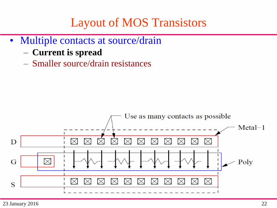
Layout of MOS Transistors
• Multiple contacts at source/drain– Current is spread
– Smaller source/drain resistances

2323 January 2016
Parasitic aware layout
• Multiple Contacts or one big contact
• Multiple contacts at source/drain
– High reliability
• Better contact at source/drain
– Smaller contact resistance
» R = Rc/N, where N=number of contacts

2423 January 2016
Layout of MOS Transistors
• Multiple contacts at source/drain– Current is spread
– Smaller source/drain resistances
• Series resistance is negligible but lateral resistance still exists.
• Large source/substrate and drain/substrate parasitic capacitances.

2523 January 2016
Layout of MOS Transistors
• Parasitics in transistor– Large gate series resistance- Gate is too long.
• Contacts are not allowed on the gate above the channel
– high temperature required to form contacts may destroy the thin gate oxide.

2623 January 2016
Layout of MOS Transistors
• Poly contact at both ends
Wide transistors need to be split

2723 January 2016
MULTI-GATE FINGER LAYOUT
• Parallel connection of n elements (n = 4 for this
example)
– Reduces the gate resistance of the poly-silicon
• Capacitance unchanged, Large area

2823 January 2016
Multifinger Layout-Shared sources/drains
• Contact space is shared among
transistors
• Reduced silicon area.
– Minimizes source/substrate &
drain/substrate parasitic
capacitances.
• important for high speed
s s sd d
Cs = ¾ Cs’
Cd = ½ Cd’
Note that parasitic
capacitors are lesser at
the drain
2923 January 2016
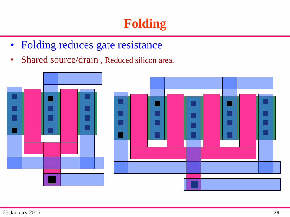
Folding
• Folding reduces gate resistance
• Shared source/drain , Reduced silicon area.

3023 January 2016
Layout of MOS Transistors
• Minimize Source/Substrate and Drain/Substrate Parasitic
Capacitances
– Shared sources/drains.
Another layout

3123 January 2016
Analog layout Issues
• Noise is important in all analog circuits because it limits
dynamic range.

3223 January 2016
Analog layout Issues
• Noise is important in all analog circuits because it limits
dynamic range.
– Body Contact
– Higher neutral body resistance
• Single Body Contact more substrate noise

3323 January 2016
Substrate contact
• Generous use of SUBSTRATE PLUGS
– help to reduce the resistance
of the neutral body region,
• Minimizes the noise
contributed by this
resistance.
– minimizes substrate noise because it provides a low impedance path to ground for the noise current

3423 January 2016
Substrate contact

3523 January 2016
Layout of a Cascode circuit
a.
b. c.
Shared Source
Drain
Shared Source
Drain-multifinger
Layout

3623 January 2016
Common Terminal

3723 January 2016 School of ECE, REVA Unversity

3823 January 2016
Antenna Effect
• Metal Etching
• There will be charge accumulation on Metal1 during plasma
etching (of metal1) causing damage to thin gate oxide (Large
metal area)

3923 January 2016
Antenna Effect
• Metal Etching
• There will be charge accumulation on Metal1 during plasma
etching (of metal1) causing damage to thin gate oxide (Large
metal area)
Avoids antenna effect

4023 January 2016
Antenna Effect
• RIE of Poly silicon

4123 January 2016
• Make connections at M1 level.

4223 January 2016
Analog layout Issues
• Matching components
– In analog electronics it is often necessary to have matched
pairs of devices with identical electrical properties, e.g. input
transistors of a differential stage, and current mirror

4323 January 2016
Layout of Matched Transistors
• Matched transistors are used extensively in both analog
and digital CMOS circuits.
– In theory two device with the same size have the same
electrical properties.

4423 January 2016
Layout of Matched Transistors
• Matched transistors are used extensively in both analog
and digital CMOS circuits.
– In theory two device with the same size have the same
electrical properties.
In reality there is always process variations

4523 January 2016
Silicon is anisotropic
• Ion implantation is performed at an angle causing
shadow
• Source and drain may not be symmetric due to ion
implantation angle,
– neccessary to avoid implant depth issues (channeling).

4623 January 2016
Photo-lithographic invariance (PLI)
• Lithography effects are different in different direction.
• Orientation is important in analog circuits for matching
purposes
– C and D are better
– Maintain orientation
C. Gate aligned
D. Parallel gate:

4723 January 2016
Photo-lithographic invariance (PLI)
• Gate aligned
• Parallel gate: – Two drains have different
surroundings
– Two sources have different
surroundings
• Current flows in the same
direction

4823 January 2016
• High energy ion implants to form the well.
• Scattering from the edge of the photoresist mask, and embedding
in the silicon surface (near well edge).
• Transistors close to the well edge will therefore have different
properties.
• This is known as the well proximity effect (WPE). Important for
matching.
School of ECE, REVA Unversity
Well Proximity Effect
As with S/D,
implantation angle may
render the scattering
and doping asymmetric

4923 January 2016
• Shallow trench isolation strains the active area of the
transistor. Influcences mobility and threshold voltage
(stress induced enhancement or suppression of dopant
diffusion).
• Distance between gate and STI impacts perfomance.
• Important for matching.
School of ECE, REVA Unversity

5023 January 2016
Matching
• Layout techniques to minimize the errors introduced by
process variations.
• Two electrically equivalent components: A and B
– Drawn identically
– A and B have same shape in
area and perimeter
– Are they Identical ?
– Do they have the same
surrounding?

5123 January 2016
Matching
• Layout techniques to minimize the errors introduced by
process variations.
• Two electrically equivalent components: A and B
– Drawn identically
– A and B have same shape in
area and perimeter
– Are they Identical ?
– Do they have the same
surrounding?
–No?

5223 January 2016
Unit Matching
• Layout techniques to minimize the errors introduced by
process variations.
• Two electrically equivalent components. A and B
– Use Dummies to have
identical surroundings

5323 January 2016
Layout of Matched Transistors
• Add dummy
transistors to
improve symmetry
• Presence of Metal line over
M2 destroys symmetry• Replicate Metal line over
M1 improves symmetry

5423 January 2016
Metal Interconnections
• Both the transistor should have same surrounding.
• Unbalanced metal routing will cause the transistors to
see different source voltage.
• Also, distribute reference as current, not bias voltage.

5523 January 2016 School of ECE, REVA Unversity

5623 January 2016
Unit matching
• Gradient along x-axis destroys symmetry

5723 January 2016
• Process variations can locally be approximated with a
linear gradient.
• Example: Desired Resistor values ; A= 7 units and B = 7
units
• Changed due to Gradient as follows.
• A= 5 units and B = 9 units
Process Variation
5 9

5823 January 2016
Process variations
• can locally be approximated with a linear gradient.
(a): A1 + A2 < B1 + B2
(b): A1 + A2 = B1 + B2 (Common-centroid layout)
2 3 4 5
2 3 4 5

5923 January 2016
Common Centroid Layouts
Cross
coupled

6023 January 2016
Common Centroid Layouts
Tiled

6123 January 2016
Common Centroid Layout
• Gradients are compensated
• Poly and metal interconnections are
complex

6223 January 2016 School of ECE, REVA Unversity

6323 January 2016
Common Centroid Layouts
• Mitigates variation in both x and Y direction

6423 January 2016

6523 January 2016M1 D
M2D
M1,2 S
M2GM1 G

6623 January 2016
Common Centroid Layout

6723 January 2016
Matched Transistors-Interdigitized Layout Style
• Inter-digitized layout style Averages the process variations among transistors
– Common terminal is like a serpentine
– Two matched transistors with one common terminal
– Split the transistor in two equal parts
– 4 fingers for each transistors, Arrange AABBAABB
2 3

6823 January 2016
M
M
1
To achieve both common-centroid
and PLI matched transistors has to
be split into 4 fingers.
M1 D
M2DM1 G
M2G
M1,2 S
M1,2 S
AABBBBAA
Matched Transistors

6923 January 2016
Matched Transistors
• Or ABBAABBA• Use dummies if needed
• Uneven total drain area between A and B.
– This is undesirable for ac conditions:
– capacitors and other parameters may not be equal
– A more robust approach
2 3

7023 January 2016
M1M2 M2M1 M1M2 M2M1 M1M2
1 2 3 4 5 6 7 8 9 10
M1 1+4+5+8+9 =27
M2 2+3 +6+7+10 = 28
Matched Transistors

7123 January 2016
Dummy Devices at the Ends
• Dummies are shorted transistors
– Adds to parasitics

7223 January 2016
Interdigital layout
• Split into parallel connections of even parts,
• Half of them will have the drain at the right side and half at the left,
• Be careful how you route the common terminal
M2 M1 M1 M2 M2 M1 M1 M2
M1 M2 M2 M1 M1 M2 M2 M1

7323 January 2016
M2 D
M1D
M2 G
M1,2 S
M1 G
M2 M1 M1 M2 M2 M1 M1 M2
M1 M2 M2 M1 M1 M2 M2 M1

7423 January 2016

7523 January 2016
Resistors
• All materials have a resistivity
• Typical resistivities
– Metal layer : 0.1 Ohm/square
– n/p-plus contacts and polysilicon: 10-100 Ohm/square
– n-well: 1000 Ohm/square
– low doped poly silicon: 10 k Ohm/square
• more well defined than n-well, i.e. higher accuracy

7623 January 2016
Poly-Resistors
• Poly Resistors– Silicidated poly resistors: 1 − 10 Ohm/sq.
• ≈±30%
– Non-silicidated poly resistors: 50-1000 Ohms per sq.
• ≈±20%
• Small parasitic capacitances to substrate.
• Superior linearity.
• High cost due to the extra mask needed to block silicide layer.

7723 January 2016
• 100-1000 Ohm/sq
– N-well
• Large error : ≈±40%
• Resistance is strongly terminal voltage-dependent and highly nonlinear.
– Depletion width varies with terminal voltages. The cross-section area varies with terminal voltages
• noisy as all disturbances/noise from substrate can be coupled directly onto the resistors
• Large parasitic capacitance between n-well and substrate.
Diffusion Resistors

7823 January 2016
• 500-2000 ohms/square
• Accuracy = ±15%
• Parasitic capacitance to substrate is voltage dependent.
• Piezoresistance effects occur due to chip strain from
mounting
Ion Implanted

7923 January 2016
• Low resistance
Metal Resistor

8023 January 2016
Resistor Layout
• Standard Resistors: Avoid 90 degree angle. 45 degree is
recommended
Recommended resistor
layout
1. Resistance at the corners cannot
be estimated accurately
2. Current flow at the corner is not
uniform

8123 January 2016
Corner Correction

8223 January 2016
Resistor Layout
• Dummy resistors are added to minimizes the effect of process
variation

8323 January 2016
Shielded Resistors
• Shielding resistors
– Connected to a constant voltage
source
• Prevent self-coupling of the
resistor R/inter-coupling
with others.
• Widely used in analog/RF
design.
• Caution
– a mutual capacitance between
the resistor and its shield exist.
Layout of shielded resistors
(S = shielding resistors)

8423 January 2016
Layout of Large Resistors
• Use n-well resistors
– have a large sheet resistance.
• Enclosed by a substrate shielding ring, also known as guard ring,
to isolate the resistors from neighboring devices.

8523 January 2016
• Process bias is where the dimensions of the fabricated
geometries are not the same as the layout data base
dimensions.
• Process biases introduce systematic errors.
Process Bias Influence on Resistors

8623 January 2016
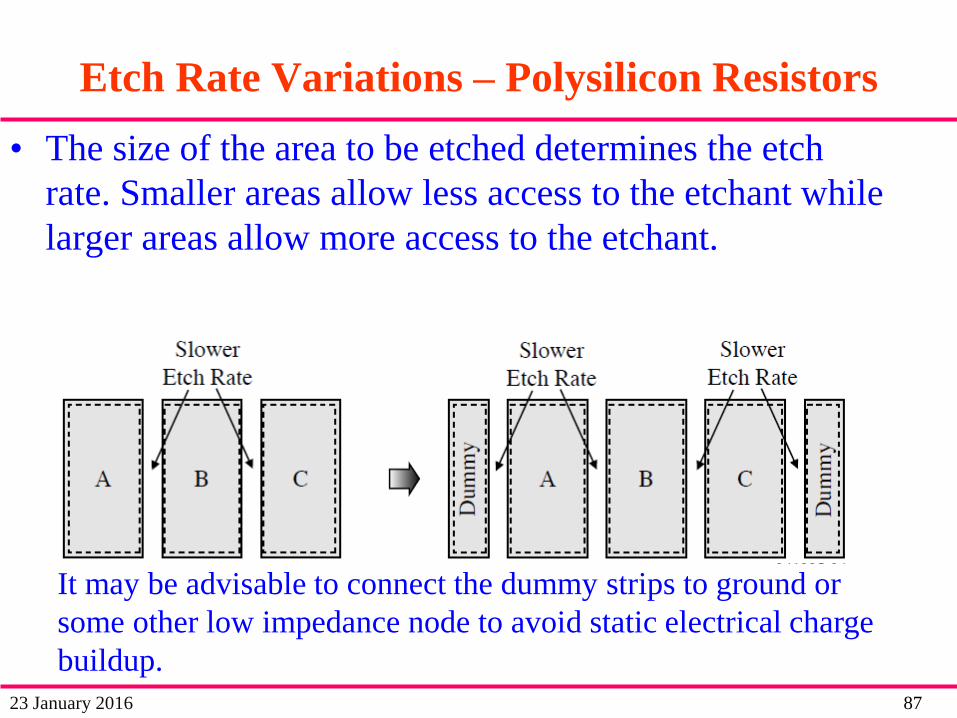
• The size of the area to be etched determines the etch
rate. Smaller areas allow less access to the etchant while
larger areas allow more access to the etchant.
Etch Rate Variations – Polysilicon Resistors
8723 January 2016
Etch Rate Variations – Polysilicon Resistors
• The size of the area to be etched determines the etch
rate. Smaller areas allow less access to the etchant while
larger areas allow more access to the etchant.
It may be advisable to connect the dummy strips to ground or
some other low impedance node to avoid static electrical charge
buildup.

8823 January 2016
• Consider three adjacent p+ diffusions into a n epitaxial
region,
• If A, B, and C are resistors that are to be matched, we see that the effective
concentration of B is larger than A or C because of diffusion interaction. This
would cause the B resistor to be smaller even though the geometry is identical.
• Solution: Place identical dummy resistors to the left of A and right of C.
Connect the dummy resistors to a low impedance to prevent the formation of
floating diffusions that might increase the sensitivity to latchup.
Diffusion Interaction – Diffused Resistors

8923 January 2016
• The thermoelectric effect, also called the Seebeck effect,
is a potential difference that is developed between two
dissimilar materials that are at different temperatures.
• Two possible resistor layouts with regard to the
thermoelectric effect:
Thermoelectric Effects

9023 January 2016
• High sheet resistivity resistors must use p+ or n+ in order to make
contacts to metal. Thus, there is plenty of opportunity for the
thermoelectric effect to cause problems if care is not taken. Below
are three high sheet resistor layouts with differing thermoelectric
performance.

9123 January 2016
• Inter-Digitized Layout
– Minimizes the effect of process variation in x-direction.
• Dummy resistors are added to ensure both resistors have
the exactly same environment.
Layout of Matched Resistors

9223 January 2016
Matched Resistors with Temperature Consideration
• Keep away from power devices

9323 January 2016
Resistor layout guidelines-Matched resistors
• Use same material
• Identical geometry, same orientation
• Close proximity, interdigitate arrayed resistors
• Use dummy elements
• Place resistors in Low stress area
• Place resistors away from power devices
• Use electrostatic shielding

9423 January 2016
Capacitors
• There are naturally capacitors between each layer of
metal, polysilicon or silicon
• Dielectrics between different metal layers have a
thickness of 0.5-1 micron, which gives a rather large
area for a given capacitance.
• Key Parameters
– Capacitance per unit area
• Larger specific capacitance (capacitance per unit area)
gives smaller area
– Linearity
– Parasitic capacitance to substrate
– Series resistance - resistance of capacitor plates

9523 January 2016
Types of IC Capacitors
• Poly-diffusion capacitors
– .6-.8 fF/µm2(≈±5%).
– Matching 0.2%
– Nonlinear bottom-plate parasitic capacitance.≈20% of inter-plate capacitance.
• MOS capacitors
– 0.6 - 0.8 fF/µm2; (≈±5%).
– Matching 0.5%
– Stable capacitance in strong inversion
– Non-negligible channel resistance lowers the quality factor (Q) of the capacitor
• Poly-poly capacitors
– 0.3 - 0.5 fF/µm2; (≈±10%). Matching 0.5%
– Not available in standard CMOS processes
• Metal-poly capacitors
– 0.03-0.05 fF/µm2. (≈±25%). Matching 0.5%
– Capacitance is small, area consuming.
• Metal-metal capacitors
– 0.02-0.04 fF/µm2; (≈±25%). Matching 0.1%
– Capacitance is small, area consuming

9623 January 2016
Pn junction capacitor
• Generally made by
diffusion into the well
• Layout: Minimize the
distance between the p+
and n+ diffusions.

9723 January 2016
MOS Gate Capacitor

9823 January 2016
Poly Poly Capacitors
• Highly stable capacitors
• small bottom plate
parasitic

9923 January 2016
• In some processes, there is a thin dielectric between a
metal layer and a special metal layer called “capacitor
top metal”. Typically the capacitance is around 1fF/μm2
and is at the level below top metal.
• Good matching is possible with low parasitics
Metal-Insulator-Metal (MiM) Capacitors

10023 January 2016
• Edge Effects
• There will always be a randomness on the definition of
the edge. However, etching can be influenced by the
presence of adjacent structures.
Capacitor Errors

10123 January 2016
NON-IDEAL EFFECTS- UNDER-CUT
• Non-uniform undercut &/or edge
fringing field effects change the
value of designed capacitors.
• The area and perimeter ratio is
preserved if we use layout
utilizing unit capacitors.
Case 1
Case 2
Ideal case: no undercut
Case 1 Case 2
Area 1:4 1:4
Perimeter 1:2 1:4
Typical case: 0.05 undercut
Case 1 Case 2
Area 1:4.46 1:4
P erimeter 1:2.1 1:4
10223 January 2016
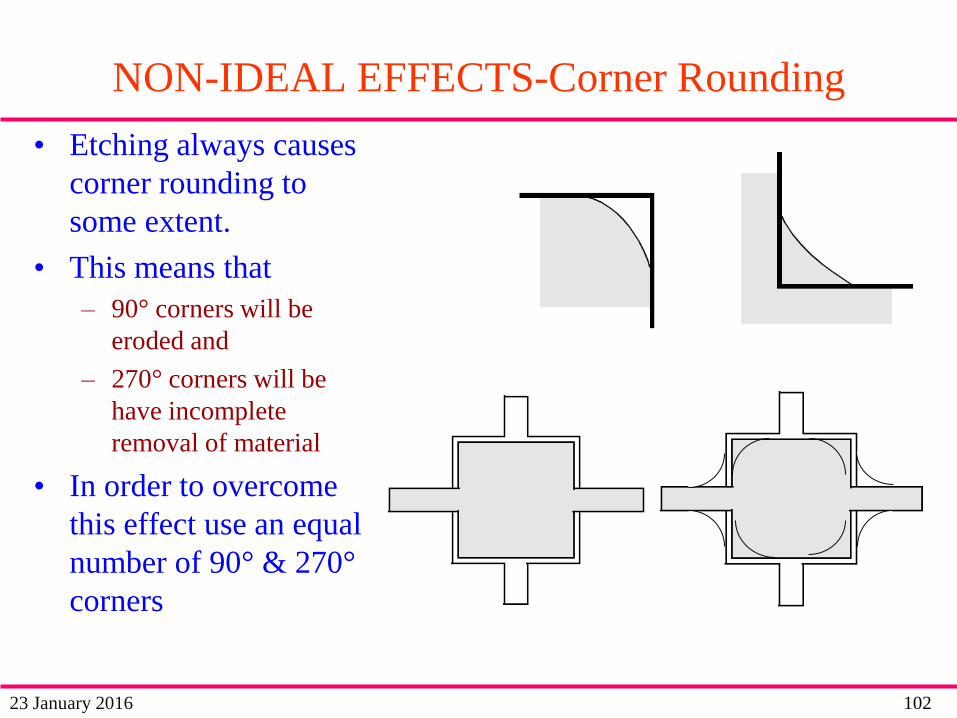
NON-IDEAL EFFECTS-Corner Rounding
• Etching always causes
corner rounding to
some extent.
• This means that
– 90° corners will be
eroded and
– 270° corners will be
have incomplete
removal of material
• In order to overcome
this effect use an equal
number of 90° & 270°
corners

10323 January 2016
Layout of Matched Capacitors
• Oxide Gradients: Error
due to a variation in
dielectric thickness across
the wafer.
• Minimize the Effect of
Oxide Thickness in both x
and y-directions.
– Common Centroid Structure.
• Dummy capacitors are
needed to ensure the same
environment for C1 and C2.

10423 January 2016
Layout of Matched Capacitors
• C1 and C2 are 2-poly capacitors.
• n-well is employed as a charge
collector to shield the interaction
between the bottom plate and
substrate.
• n-well is biased at multiple
points and connected to a
constant voltage source.

10523 January 2016
Are there any thing else you can improve?
Is there full symmetry between C1 and C2?

10623 January 2016
Decreasing Sensitivity to Edge Variation
Sensitive to alignment errors in
the upper and lower plates and
loss of capacitance flux (smaller
capacitance).
Insensitive to alignment errors
and the flux reaching the bottom
plate is larger resulting in large
capacitance.
A structure that minimizes the ratio of perimeter to area (circle is
best).

10723 January 2016
• Accurate matching of capacitors depends on the
following influence:
– Mismatched perimeter ratios
– Proximity effects in unit capacitor photolithography
– Mismatched long-range fringe capacitance
– Mismatched interconnect capacitance
– Parasitic interconnect capacitance
Accurate Matching of Capacitors

10823 January 2016
• Long-range fringe capacitance
Long-range fringe capacitance
:

10923 January 2016
References
• A. Hastings, The Art of Analog Layout, Prentice-
Hall,2002.
• B. Razavi, Design of Analog CMOS Integrated Circuits,
McGraw-Hill, 2001.

11023 January 2016
Summary
• Use large area to reduce random error
• Common Centroid layout to reduce linear gradient errors
• Use unit element arrays
• Interdigitize for matching
• Use of symmetry (photolithographic invariance)
• Dummy device for similar vicinity
• Guard rings for isolation
11123 January 2016
Thank You