introduction: basics of microscopy (tem) thomas … · 2017-11-10 · using electron static and ......
TRANSCRIPT
11/10/2017
1
Thomas LaGrange, Ph.D.
Faculty Lecturer and
Senior Staff Scientist
[email protected] www.epfl.ch cime.epfl.ch +41 (0)21 6934430
Introduction: Basics of
Transmission Electron
Microscopy (TEM)
TEM Doctoral Course MS-637
Nov. 13-15th, 2017
[email protected] www.epfl.ch cime.epfl.ch +41 (0)21 6934430
Outline
1. What is microcopy?
2. Why do we use electrons as a probe?
3. Electron-matter interactions in a thin sample
4. Components of the TEM
5. TEM imaging modes
11/10/2017
2
[email protected] www.epfl.ch cime.epfl.ch +41 (0)21 6934430
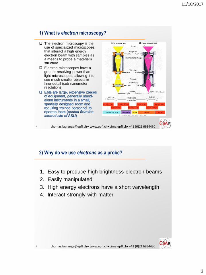
1) What is electron microscopy?
The electron microscopy is the use of specialized microscopes that interact a high energy electron beam with samples as a means to probe a material’s structure
Electron microscopes have a greater resolving power than light microscopes, allowing it to see much smaller objects in finer detail (sub nanometer resolution)
3
[email protected] www.epfl.ch cime.epfl.ch +41 (0)21 6934430
1. Easy to produce high brightness electron beams
2. Easily manipulated
3. High energy electrons have a short wavelength
4. Interact strongly with matter
4
2) Why do we use electrons as a probe?
11/10/2017
3
[email protected] www.epfl.ch cime.epfl.ch +41 (0)21 6934430
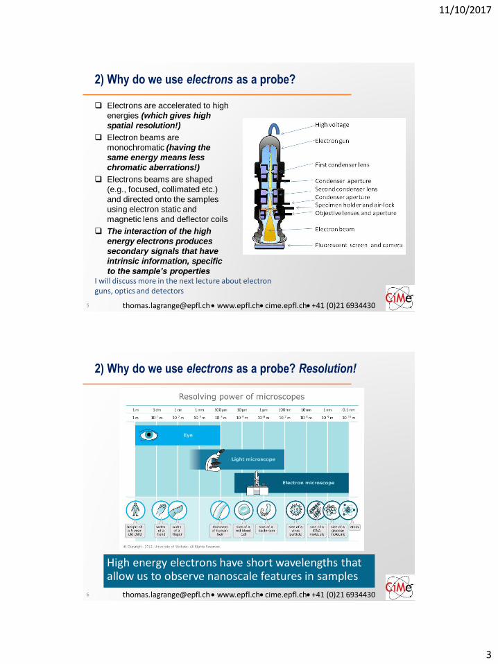
2) Why do we use electrons as a probe?
Electrons are accelerated to high
energies (which gives high
spatial resolution!)
Electron beams are
monochromatic (having the
same energy means less
chromatic aberrations!)
Electrons beams are shaped
(e.g., focused, collimated etc.)
and directed onto the samples
using electron static and
magnetic lens and deflector coils
The interaction of the high
energy electrons produces
secondary signals that have
intrinsic information, specific
to the sample’s properties
5
I will discuss more in the next lecture about electron guns, optics and detectors
[email protected] www.epfl.ch cime.epfl.ch +41 (0)21 6934430
2) Why do we use electrons as a probe? Resolution!
High energy electrons have short wavelengths that allow us to observe nanoscale features in samples
6
11/10/2017
4
[email protected] www.epfl.ch cime.epfl.ch +41 (0)21 6934430
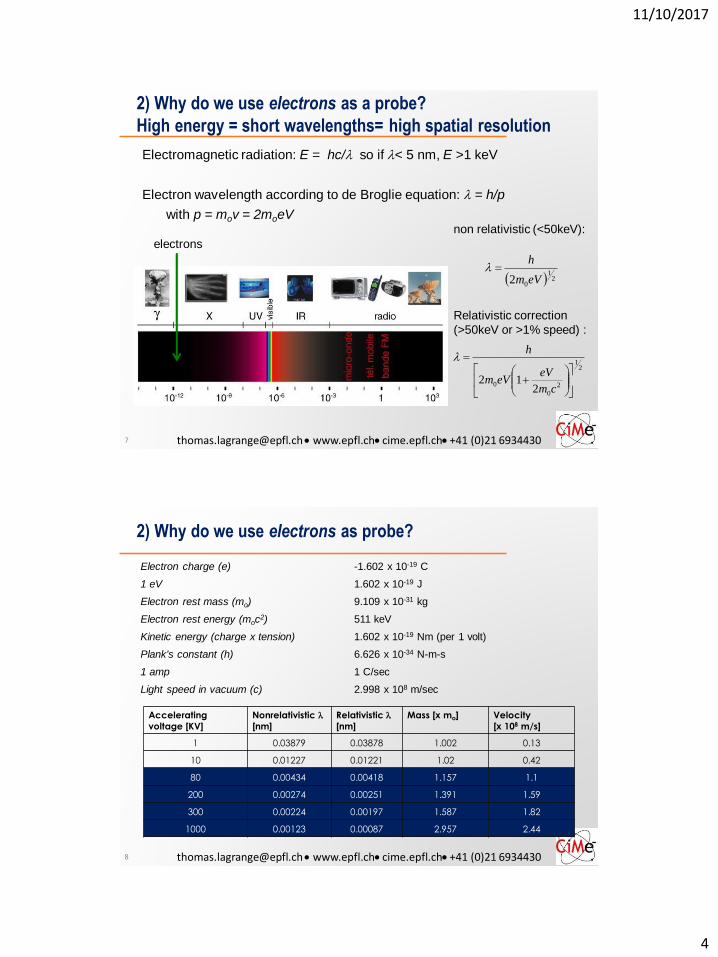
2) Why do we use electrons as a probe?
High energy = short wavelengths= high spatial resolution
7
electrons
Electromagnetic radiation: E = hc/ so if < 5 nm, E >1 keV
Electron wavelength according to de Broglie equation: = h/p
with p = mov = 2moeV non relativistic (<50keV):
Relativistic correction
(>50keV or >1% speed) :
21
02 eVm
h
21
2
0
02
12
cm
eVeVm
h
[email protected] www.epfl.ch cime.epfl.ch +41 (0)21 6934430
2) Why do we use electrons as probe?
8
Electron charge (e) -1.602 x 10⁻¹⁹ C
1 eV 1.602 x 10⁻¹⁹ J
Electron rest mass (mo) 9.109 x 10⁻³¹ kg
Electron rest energy (moc2) 511 keV
Kinetic energy (charge x tension) 1.602 x 10⁻¹⁹ Nm (per 1 volt)
Plank's constant (h) 6.626 x 10⁻³⁴ N-m-s
1 amp 1 C/sec
Light speed in vacuum (c) 2.998 x 10⁸ m/sec
Accelerating
voltage [KV]
Nonrelativistic
[nm]
Relativistic
[nm]
Mass [x mo] Velocity
[x 108 m/s]
1 0.03879 0.03878 1.002 0.13
10 0.01227 0.01221 1.02 0.42
80 0.00434 0.00418 1.157 1.1
200 0.00274 0.00251 1.391 1.59
300 0.00224 0.00197 1.587 1.82
1000 0.00123 0.00087 2.957 2.44

11/10/2017
5
[email protected] www.epfl.ch cime.epfl.ch +41 (0)21 6934430
2) Why do we use electron as a probe?
9
Green light : ≈ 532 nm,
(objective collection angle)~1 rad
n= 1.7 for oil immersion lens
*** d=200nm
Electrons 200 keV : ≈ 0.00251nm
n=1 for vacuum
max =0.1 rad given TEM geometry
***d=0.015 nm
Lens aberrations limit spatial
resolution
Spherical and Chromatic
Aberration corrections allow for
0.05 nm resolution
𝑑 = 0.61
𝑛 sin 𝜃= 0.61
𝜆
𝛽
𝑑
Raleigh’s Criterion
Airy Diffraction Disks
[email protected] www.epfl.ch cime.epfl.ch +41 (0)21 6934430
2) Why do we use electrons as probe?
Without Cs correction,
optimal convergence angle
and resolution are given by:
2.5x10⁻¹² m @ 200 kV
1-10 mrad
d (spatial resolution) is
0.2-3 nm
S. J. Pennycook & al., in: The Oxford Handbook of Nanoscienceand Nanotechnology, ed. A. V. Narlikar and Y. Y. Fu, OxfordUniversity Press, Oxford, United Kingdom, 2010, p. 205.
Higher convergence angle
produces more aberrations
which lower spatial resolution.
With Cs Correction:
d is 0.06 to 0.07 nm
11/10/2017
6
[email protected] www.epfl.ch cime.epfl.ch +41 (0)21 6934430 11
Why do we use electrons as probe?
Electrons interact strongly with matter
[email protected] www.epfl.ch cime.epfl.ch +41 (0)21 6934430
3) Electron-matter interactions in a thin sample
Interaction of electrons with the sample
Specimen
Inc
ide
nt b
ea
m
Backscattered electrons
BSE
secondary electrons
SE
Characteristic
X-rays visible light
“absorbed” electrons electron-hole pairs
elastically scattered
electrons
dir
ec
t b
ea
m
inelastically
scattered electrons
Bremsstrahlung
X-rays
1-100 nm
11/10/2017
7
[email protected] www.epfl.ch cime.epfl.ch +41 (0)21 6934430
3) Electron-matter interactions in a thin sample
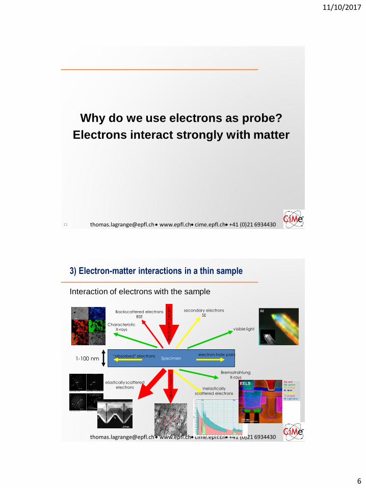
Two Categories of electrons
1. Elastically scattered Coherent
Bragg diffracted electrons
(selected area electron diffraction, bright-field, dark-field, weak beam)
Phase Contrast imaging (HRTEM)
Incoherent Mass-thickness contrast imaging
Z-Contrast imaging (HAADF STEM)
Backscattered electrons
2. Inelastically scattered Secondary signals
Characteristic X-rays and Bremsstrahlung
Visible light (CL)
Auger electrons
Incoherent Secondary Electrons
Electron Energy Loss Spectroscopy (EELS)
13
[email protected] www.epfl.ch cime.epfl.ch +41 (0)21 6934430
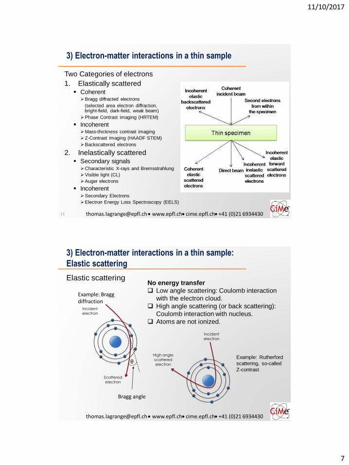
3) Electron-matter interactions in a thin sample:
Elastic scattering
Elastic scattering
Incident
electron
Scattered
electron
θ
No energy transfer
Low angle scattering: Coulomb interaction
with the electron cloud.
High angle scattering (or back scattering):
Coulomb interaction with nucleus.
Atoms are not ionized.
Incident
electron
High angle
scattered
electron
Example: Rutherford
scattering, so-called
Z-contrast
Example: Bragg diffraction
Bragg angle

11/10/2017
8
[email protected] www.epfl.ch cime.epfl.ch +41 (0)21 6934430
3) Electron-matter interactions in a thin sample:
Electron Diffraction
dhkl = n /2 sinq
kk’
g = k-k’
Elastic diffraction
|k| = |k’|
Periodic arrangement of atoms in the real space:
g : vector in the reciprocal space
The Bragg's law
Bragg diffraction occurs when radiation,
with a wavelength comparable to the
atomic spacing, is scattered by the atom
centers and undergoes constructive
interference. The path difference, dhkl,
associated to the scattering angle, θ, is
given by
**Dr. Duncan Alexander will discuss this topic in
detail in his lectures this afternoon.
q
[email protected] www.epfl.ch cime.epfl.ch +41 (0)21 6934430
Nickel based
superalloys
Contrast /’
3) Electron-matter interactions in a thin sample:
Diffraction Contrast imagingUsing Bragg diffracted electrons, you can generate
1. Diffraction patterns, which have crystallographic information, i.e., crystal symmetry, lattice parameters, atom postions, etc…
2. Bright-field images that hold information about morphology, grain size, defect structures, etc…
3. Dark-field images, which can be used to correlate crystalline phase and orientation to grain morphologies, distribution with the microstructure, defect structures, etc.
Bright-field TEM image Dark-field TEM image

11/10/2017
9
[email protected] www.epfl.ch cime.epfl.ch +41 (0)21 6934430
Phase contrast for crystalline specimen
Sounds simple:
Crystal structure
properly oriented
Electron beam
Projected image
Objective
lens
Si [110] orientation
3) Electron-matter interactions in a thin sample:
Phase Contrast and HRTEM
**HRTEM will be
discussed in more
detail in lectures on
Tuesday
[email protected] www.epfl.ch cime.epfl.ch +41 (0)21 6934430
Unfortunately things are
much more complicated
Mixing of information from the sample
and microscope via INTERFERENCES!
Direct and Diffracted beams (Phase shift!)
Objective lens (with aberrations affects phase shifts)
Projected amplitude after intereference!
Electron beam
3) Electron-matter interactions in a thin
sample: Phase Contrast and HRTEM
Crystal thickness with a given orientation
affects phase and amplitude of the beam
in a complicated way
11/10/2017
10
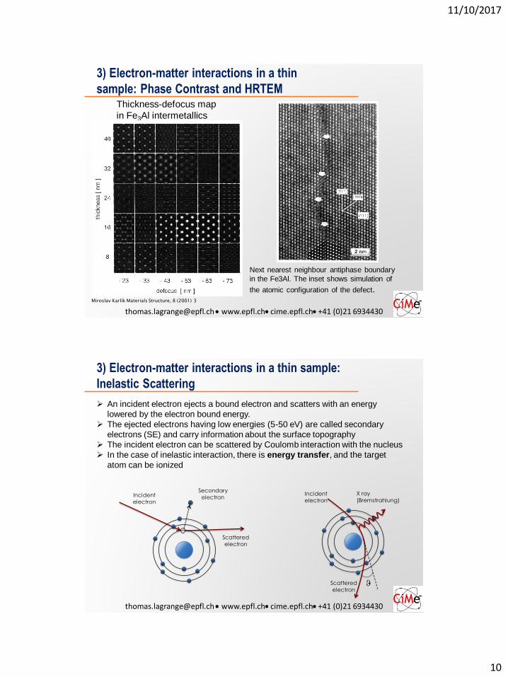
[email protected] www.epfl.ch cime.epfl.ch +41 (0)21 6934430
Thickness-defocus map
in Fe3Al intermetallics
Miroslav Karlík Materials Structure, 8 (2001) 3
Next nearest neighbour antiphase boundary
in the Fe3Al. The inset shows simulation of
the atomic configuration of the defect.
3) Electron-matter interactions in a thin
sample: Phase Contrast and HRTEM
[email protected] www.epfl.ch cime.epfl.ch +41 (0)21 6934430
3) Electron-matter interactions in a thin sample:
Inelastic Scattering
Incident
electron
Secondary
electron
Scattered
electron
An incident electron ejects a bound electron and scatters with an energy
lowered by the electron bound energy.
The ejected electrons having low energies (5-50 eV) are called secondary
electrons (SE) and carry information about the surface topography
The incident electron can be scattered by Coulomb interaction with the nucleus
In the case of inelastic interaction, there is energy transfer, and the target
atom can be ionized
Incident
electron
Scattered
electronJ
X ray
(Bremstrahlung)

11/10/2017
11
[email protected] www.epfl.ch cime.epfl.ch +41 (0)21 6934430
Mass Thickness Contrast: Incoherent elastic
scattering that results form
the difference in the
atomic number (Z) and/or
thickness (t)
Scattering is proportional
to Z2 t
Higher-Z or thicker areas
will appear darker in
bright-field TEM mode
Being incoherent, this
contrast mechanism
applies to both crystalline
and amorphous materials
Mass thickness Contrast examples: Hollow polymer spheres with different wall thicknesses
3) Electron-matter interactions in a thin sample:
Incoherent elastic scattering – Mass thickness
[email protected] www.epfl.ch cime.epfl.ch +41 (0)21 6934430
High-angle annular dark-field =>
compositional contrast:
intensity ∝ Z2t
(thickness t, atomic number Z)
Pt catalyst on Al2O3 Si-Ge/Si multilayer
Cs-orcrected - graphene with
dopant atoms (Krivanek et al., Nion)
Focused e- probe scanned on
sample; disc and annular detectors
in back focal (diffraction) plane
Scan beam
EELS spectrometer
Z-contrast examples:
3) Electron-matter interactions in a thin
sample: Incoherent elastic scattering - STEM

11/10/2017
12
[email protected] www.epfl.ch cime.epfl.ch +41 (0)21 6934430
3) Electron-matter interactions in a thin sample:
Inelastic Scattering
Electron absorption
– atom displacement ("knock on") • Radiation damage
– chemical bound breaking• Radiolysis
– lattice atom vibrations (phonons) • Sample heating
– charge collective oscillation excitation (plasmons)
– excitation of surface electronic level (transition
valence/conduction,...)
– core atomic level excitation (ionization)
– Bremsstrahlung radiation
– the relative impact of these various interaction mechanisms varies
with the type of material (no simple modelling of absorption)
[email protected] www.epfl.ch cime.epfl.ch +41 (0)21 6934430
3) Electron-matter interactions in a thin sample:
Inelastic Scattering
Relaxation processes of the excited state
Characteristic X ray
X-ray generationX ray energy
characteristic
interorbital electron
transitions and thus
of the element
Visible photon
FluorescenceLow transition
energy, visible
or UV photon is
emitted
Auger electron
Emission AugerThe relaxing process
interacts with an electron
with a characteristic energy
11/10/2017
13
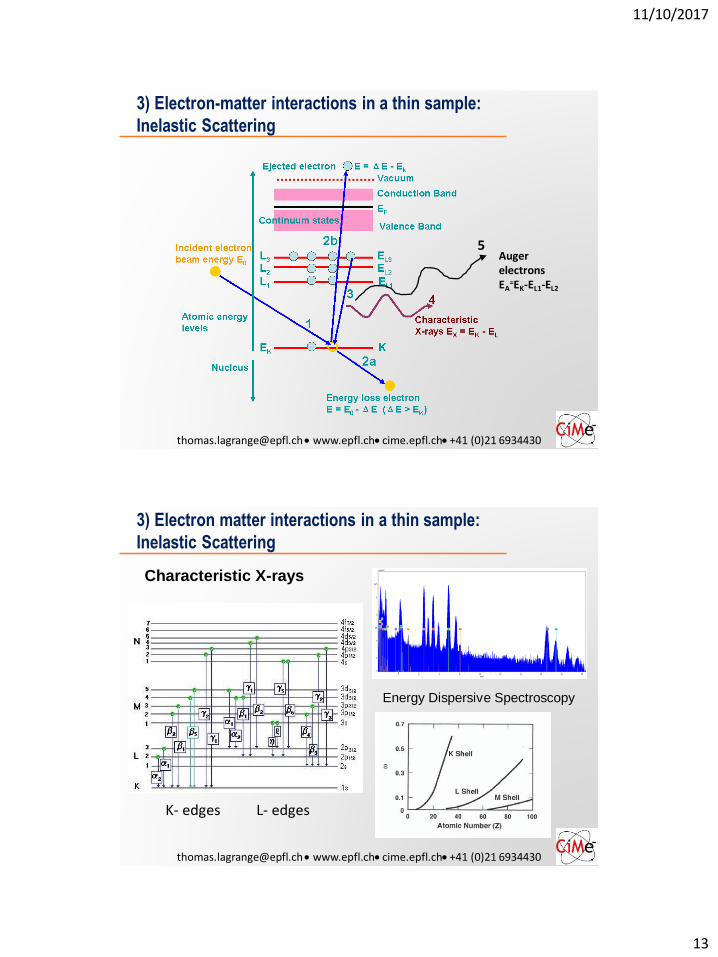
[email protected] www.epfl.ch cime.epfl.ch +41 (0)21 6934430
3) Electron-matter interactions in a thin sample:
Inelastic Scattering
5Auger electronsEA
=EK-EL1-EL2
[email protected] www.epfl.ch cime.epfl.ch +41 (0)21 6934430
3) Electron matter interactions in a thin sample:
Inelastic Scattering
Energy Dispersive Spectroscopy
K- edges L- edges
Characteristic X-rays

11/10/2017
14
[email protected] www.epfl.ch cime.epfl.ch +41 (0)21 6934430
3) Electron matter interactions in a thin sample:
Inelastic Scattering
Scanning TEM EDS mapping
TiNbNcoating
CoCrMosubstrate
[email protected] www.epfl.ch cime.epfl.ch +41 (0)21 6934430
3) Electron-matter interactions in a thin sample:
Inelastic Scattering
Interaction with plasmons and core losses
Plasmons are collective oscillations of weakly bound
electrons – plasmon losses dominate in materials with “free
electron” bonding (can be used to calculate thickness)
Core losses (atom ionization) depends on atomic species
and thus carries some chemical information about the
sample as well as bonding, valance states, density of states
(pre-edge ELNES), near neighbour coordination (post edge,
EXEFS), etc.
11/10/2017
15
[email protected] www.epfl.ch cime.epfl.ch +41 (0)21 6934430
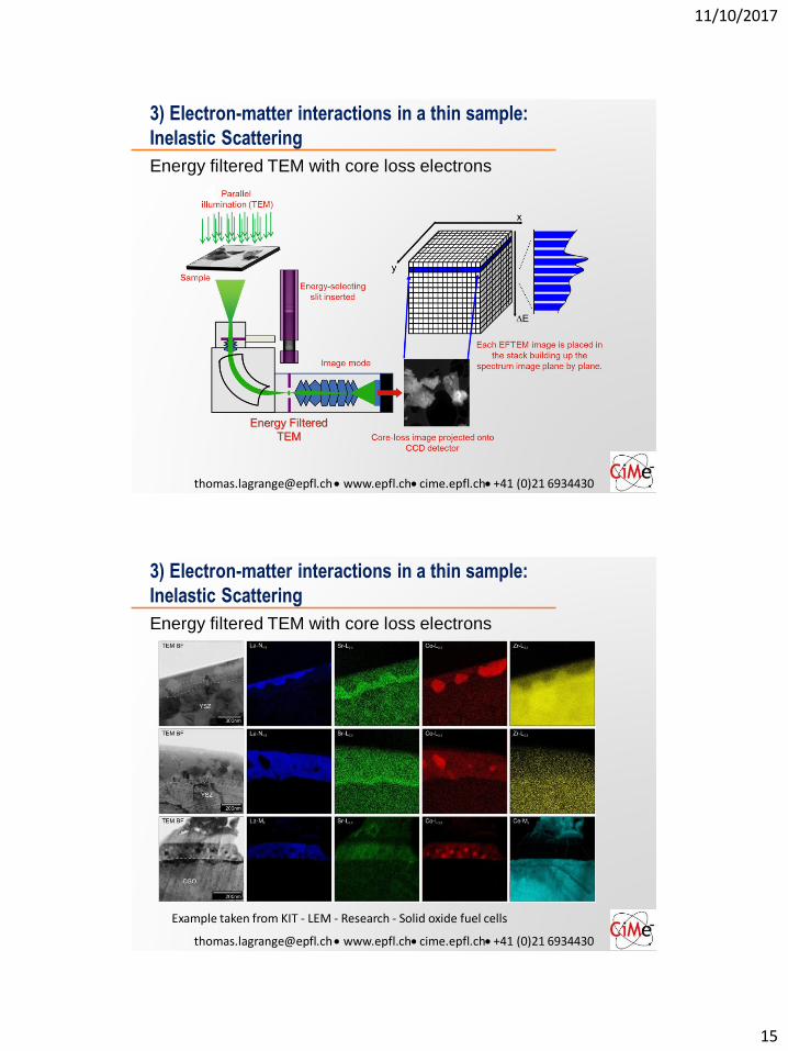
3) Electron-matter interactions in a thin sample:
Inelastic Scattering
Energy filtered TEM with core loss electrons
[email protected] www.epfl.ch cime.epfl.ch +41 (0)21 6934430
3) Electron-matter interactions in a thin sample:
Inelastic Scattering
Energy filtered TEM with core loss electrons
Example taken from KIT - LEM - Research - Solid oxide fuel cells

11/10/2017
16
[email protected] www.epfl.ch cime.epfl.ch +41 (0)21 6934430
3) Electron-matter interactions in a thin sample:
Catholuminescence
Electron-holes creation:
An incident electron onto a semiconductor can excite a valence electron to the conduction band, creating an electron-hole pair.
Cathodoluminescence:
The excited electron recombines with its hole, emitting a photon with energy equal to the band gap, that is usually in visible range. This technique can be used to understand how defects modify the band gap in nanostructures.
Egap
Conduction band
Valence band
Electron incident
Egap
Conduction band
Valence band
Conduction band
Valence band
Electron with the associated energy loss
Eg =hn
[email protected] www.epfl.ch cime.epfl.ch +41 (0)21 6934430
Summary
Why do we use electrons as probe?
32
1. Easy to produce high brightness electron beams
High coherence beams allow us to generate diffraction patterns and high spatial resolution images
2. Easily manipulated
Electron lenses and deflectors can used to easily change focal lengths and beam directions which is a necessary operating condition for flexible imaging devices
3. High energy electrons have a short wavelength
Shorter wavelengths means higher spatial resolution (Raleigh Criterion)
4. Electrons interact strongly with matter
Secondary signals have information specific to the material
Bragg diffracted electrons –structure, orientation, phase distribution, defect content and structures, etc.

11/10/2017
17
[email protected] www.epfl.ch cime.epfl.ch +41 (0)21 6934430
4) Components of the TEM
1. Electron Source
2. Sample
Illumination
(Condenser
lenses)
3. Imaging lens
(Objective)
4. Magnification and
projection
(intermediate and
projector lenses)
5. Detectors
a detector (eye,
photographic
plate, video
camera...
an illumination
section (lenses,
apertures...)
a magnification
section
(lenses, apertures...)
a sample
(+ a
"goniometer")
A "light"
source
[email protected] www.epfl.ch cime.epfl.ch +41 (0)21 6934430
4) Components of the TEM
A typical TEM: Jeol 200cx
Electron gun : generates and
accelerates the electrons to the
desired energy (velocity)
Filament: emits the electrons
Accelerator stage: accelerates
them to high energies >60keV
Unit W LaB6 FEG Cold
FEG
Brightness A/m2s
r
1010 5.1011 5.1012 1013
Cross over
size
nm 105 104 15 3
E-spread eV 3 1.6 0.7 0.3
vacuum Pa 10-2 10-4 10-6 10-9
Lifetime h 100 1000 >5000 >5000
1. Electron Source
11/10/2017
18
[email protected] www.epfl.ch cime.epfl.ch +41 (0)21 6934430
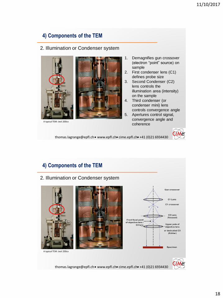
4) Components of the TEM
A typical TEM: Jeol 200cx
2. Illumination or Condenser system
1. Demagnifies gun crossover
(electron “point” source) on
sample
2. First condenser lens (C1)
defines probe size
3. Second Condenser (C2)
lens controls the
illumination area (intensity)
on the sample
4. Third condenser (or
condenser mini) lens
controls convergence angle
5. Apertures control signal,
convergence angle and
coherence
[email protected] www.epfl.ch cime.epfl.ch +41 (0)21 6934430
4) Components of the TEM
A typical TEM: Jeol 200cx
2. Illumination or Condenser system

11/10/2017
19
[email protected] www.epfl.ch cime.epfl.ch +41 (0)21 6934430
4) Components of the TEM
3. Objective lens (forms the image!)
Specimen (object)
Objective lens
Back focal plane : diffraction patternObjective Aperture
Image (first intermediate)
Image plane : Selected AreaAperture
DiffractedBeams
[email protected] www.epfl.ch cime.epfl.ch +41 (0)21 6934430
4) Components of the TEM
3. Objective lens
(forms the image!)
Eucentric Focus is the “standard” or
optimal objective lens current (focus)
Eucentric height/plane is the optimal
specimen position at the objective
lens standard focus
Image will appear over or under focus if
specimen is not at the eucentric plane

11/10/2017
20
[email protected] www.epfl.ch cime.epfl.ch +41 (0)21 6934430
4) Components of the TEM
A typical TEM: Jeol 200cx
4. Intermediate and Projector lenses1. Intermediate lenses are
used to switch between
imaging & diffraction mode
2. Intermediate lenses are
used to change
magnification and camera
length, i.e., objective lens
current.
3. Three intermediate lenses
are necessary to
compensate for the
spiraling of electrons and
resulting image rotation
4. Projector lens used to
greatly magnify the last
intermediate lens image
plane onto the detector
[email protected] www.epfl.ch cime.epfl.ch +41 (0)21 6934430
4) Components of the TEM
4. Intermediate and Projector lenses

11/10/2017
21
[email protected] www.epfl.ch cime.epfl.ch +41 (0)21 6934430
4) Components of the TEM
Apertures Small, 10-200 m holes (generally
4 to 8 sizes to chose from) limiting
the beam diameter in specific
imaging planes and lens crossovers
to change properties of illuminating
electron beam or specimen
scattered electrons
1. Condenser (2): used to change
probe size, convergence angle
and electron beam coherence
2. Objective: used to form
diffraction (and phase) contrast
images and other type images
by omitting scattered beams
3. Selected Area: used to limit or
select the region which
contributes to the electron
diffraction pattern
[email protected] www.epfl.ch cime.epfl.ch +41 (0)21 6934430
4) Components of the TEM
4. Detectors 1. Phosphor screen
2. Film
3. Image plates
4. CCD or CMOS cameras
5. YAG scintillator –
multichannel plates
6. Phosphor –
photomultipler tube
7. X-ray detectors
8. BSE, SE, STEM
detectors
I will discuss more in the next lecture about electron guns, optics and detectors
11/10/2017
22
[email protected] www.epfl.ch cime.epfl.ch +41 (0)21 6934430
Summary
Components of a TEM
43
1. Electron SourceProduces high energy, large current, and high coherence electron
beams necessary for generating diffraction patterns and high spatial
resolution images
2. Condenser lenses
Controls spot size and illumination area on sample (beam intensity)
3. Objective lens
Images sample and is strongest lens in the system
4. Intermediate and projector lenses
Changes modes from diffraction to imaging
Controls magnification
5. Detectors
Various different configurations designed to collect secondary signals
produced by the high-energy electron beam
[email protected] www.epfl.ch cime.epfl.ch +41 (0)21 6934430
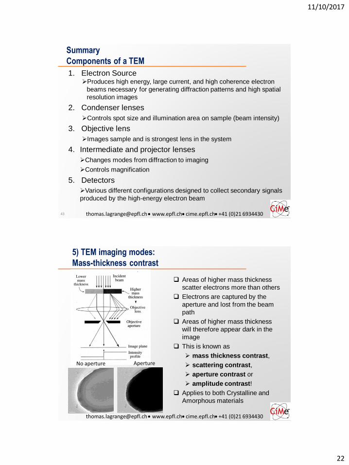
5) TEM imaging modes:
Mass-thickness contrast
Areas of higher mass thickness
scatter electrons more than others
Electrons are captured by the
aperture and lost from the beam
path
Areas of higher mass thickness
will therefore appear dark in the
image
This is known as
mass thickness contrast,
scattering contrast,
aperture contrast or
amplitude contrast!
Applies to both Crystalline and
Amorphous materials
No aperture Aperture

11/10/2017
23
[email protected] www.epfl.ch cime.epfl.ch +41 (0)21 6934430
5) TEM imaging modes:
Fresnel contrast – phase contrast
Fresnel fringes
1-2) Under-focused, uniform
white fringes
3) Focussed, min of
contrast, no fringes
4-5) Over-focused, uniform
dark fringes
Fringes arise due to the high coherence of the
electron beam and interface of two electron waves,
one which is not scattered (vacuum) and one that
scatters off the edges of sample features (the hole in
this example), resulting in a path length difference
and modulation with that has a fringe contrast.
Light or dark fringe thickness depends on focus!
1) 2) 3)
4) 5)
[email protected] www.epfl.ch cime.epfl.ch +41 (0)21 6934430
5) TEM imaging modes:
Fresnel contrast
1) Good Astigmatism,
uniform fringe
2) Bad Astigmatism,
non-uniform fringe
Fresnel fringes can
also be used to
observe and correct
the astigmatism of the
objective lens.
Astigmatic Image
Non-uniform
Fresnel Fringe
1) 2)

11/10/2017
24
[email protected] www.epfl.ch cime.epfl.ch +41 (0)21 6934430
5) TEM imaging modes:
Fresnel contrast
47
a) Under-focused,
dark core
b) Over-focused,
2 dark fringes and
white core
c) Measured wire width
ZZ at under-focused
condition
d) Measured wire width
ZZ at over-focused
condition
Note!! ZZZZ**
**
Width of Fresnel fringes depends on the thickness, defocus,
beam properties and lens aberrations.
Do not use them to assist in measuring particles sizes unless
you have calculated how they relate to the true particle size!
[email protected] www.epfl.ch cime.epfl.ch +41 (0)21 6934430
5) TEM imaging modes
Diffraction mode
The intermediate and
projector lens magnify and
project the back focal
plane (first diffraction
pattern formed in the
microscope) of the
objective lens to the
detector system
Imaging mode
The intermediate and
projector lens magnify and
project the image plane of
the objective lens to the
detector system
11/10/2017
25
[email protected] www.epfl.ch cime.epfl.ch +41 (0)21 6934430
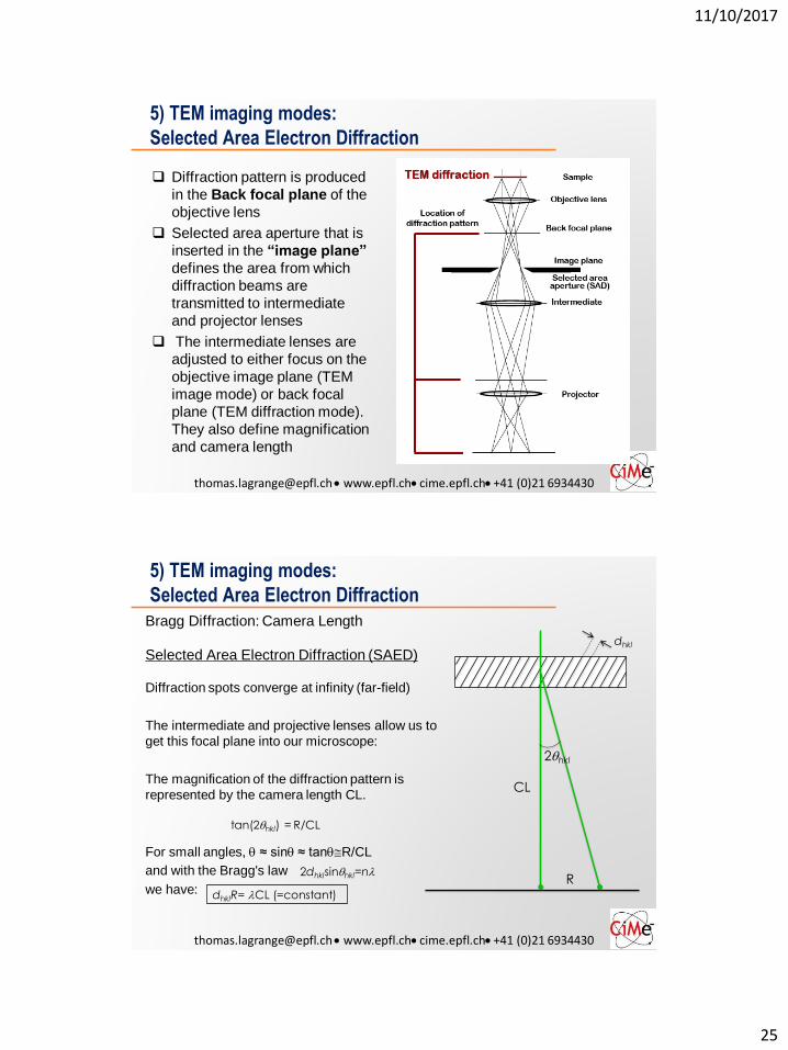
5) TEM imaging modes:
Selected Area Electron Diffraction
Diffraction pattern is produced
in the Back focal plane of the
objective lens
Selected area aperture that is
inserted in the “image plane”
defines the area from which
diffraction beams are
transmitted to intermediate
and projector lenses
The intermediate lenses are
adjusted to either focus on the
objective image plane (TEM
image mode) or back focal
plane (TEM diffraction mode).
They also define magnification
and camera length
[email protected] www.epfl.ch cime.epfl.ch +41 (0)21 6934430
Bragg Diffraction: Camera Length
Selected Area Electron Diffraction (SAED)
Diffraction spots converge at infinity (far-field)
The intermediate and projective lenses allow us to
get this focal plane into our microscope:
The magnification of the diffraction pattern is
represented by the camera length CL.
For small angles, q ≈ sinq ≈ tanqR/CL
and with the Bragg's law
we have:
tan(2qhkl) = R/CL
dhklR= CL (=constant)
2dhklsinqhkl=nR
CL
dhkl
2qhkl
5) TEM imaging modes:
Selected Area Electron Diffraction

11/10/2017
26
[email protected] www.epfl.ch cime.epfl.ch +41 (0)21 6934430
5) TEM imaging modes:
Selected Area Electron Diffraction
Bragg DiffractionPowder diagram
111
200
220
311
222 Right image is diffraction pattern from
a fine grained material (Polycrystalline
TiCl fcc calibration sample) that
produces “rings” if the selected area
is large
Scattering from angles which undergo
constructive interference or
“reflections” (i.e. all atomic planes with
non-zero intensity in the structure
factor) are present
Powder patterns are also called "ring
or powder pattern"
Angular relations between the atomic
planes are lost in powder patternsLarge grains or single
crystals produce spot
patterns
[email protected] www.epfl.ch cime.epfl.ch +41 (0)21 6934430
5) TEM imaging modes:
Selected Area Electron DiffractionDiffraction pattern indexing
Indexing is used to determine phase and orientation
Cubic system can be done by hand but more
complex crystal structures require simulations and
software
Simulations: Software JEMS (P. Stadelmann), e.g.,
calulates orientation of a known structure and
compares with experimental diffraction pattern.
11/10/2017
27
[email protected] www.epfl.ch cime.epfl.ch +41 (0)21 6934430
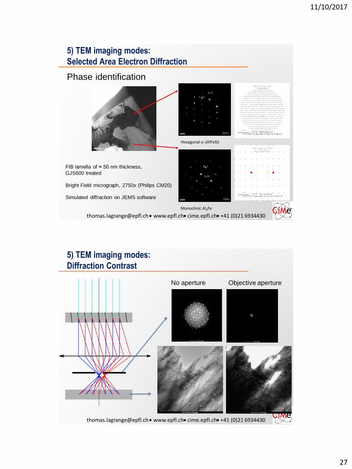
5) TEM imaging modes:
Selected Area Electron Diffraction
Phase identification
FIB lamella of ≈ 50 nm thickness,
GJS600 treated
Bright Field micrograph, 2750x (Philips CM20)
Simulated diffraction on JEMS software
Hexagonal -(AlFeSi)
Monoclinic Al3Fe
40-3
0-20
[304]
[831]
0-13
1-2-2
[email protected] www.epfl.ch cime.epfl.ch +41 (0)21 6934430
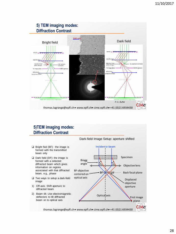
No aperture Objective aperture
5) TEM imaging modes:
Diffraction Contrast
11/10/2017
28
[email protected] www.epfl.ch cime.epfl.ch +41 (0)21 6934430
Bright field Dark field100 nm
P.-A. Buffat
5) TEM imaging modes:
Diffraction Contrast
[email protected] www.epfl.ch cime.epfl.ch +41 (0)21 6934430
5)TEM imaging modes:
Diffraction Contrast
Dark-field Image Setup: aperture shifted
Bright fied (BF) : the image is
formed with the transmitted
beam only
Dark field (DF): the image is
formed with a selected
diffracted beam which gives
information on regions
associated with that diffracted
beam, e.g., phase
Two ways to setup a dark-field
image
1) Off-axis: Shift aperture to
diffracted beam
2) Beam tilt: Use electromagnetic
deflectors to tilt diffracted
beam on to optical axis
Incident e-beam
Specimen
Objective lens
Back focal plane
First imageplane
BF DF
Displaced objective aperture
Bragg angle 2qB 2qB
Optical axis
BF objective centered on optical axis

11/10/2017
29
[email protected] www.epfl.ch cime.epfl.ch +41 (0)21 6934430
5)TEM imaging modes:
Diffraction Contrast
Dark-field Image Setup: beam tilted
Bright fied (BF) : the image is
formed with the transmitted
beam only
Dark field (DF): the image is
formed with a selected
diffracted beam which gives
information on regions
associated with that diffracted
beam, e.g., phase
Two ways to setup a dark-field
image
1) Off-axis: Shift aperture to
diffracted beam
2) Beam tilt: Use electromagnetic
deflectors to tilt diffracted
beam on to optical axis
Specimen
Objective lens
Back focal plane
First imageplane
Tilt incidente-beam by –2𝜃B
DF
Bragg angle
Optical axis
DF objective centered on optical axis
2qB2qB
2qB
[email protected] www.epfl.ch cime.epfl.ch +41 (0)21 6934430
5)TEM imaging modes:
Diffraction Contrast
Beam Tilted
Which method produces fewer distortions, i.e., has
spatial resolution, off-axis or beam tilt method?
Aperture Shifted
Specimen
Objective lens
Back focal plane
First imageplane
Tilt incidente-beam by –2𝜃B
DF
Bragg angle
Optical axis
objective centered on optical axis
Incident e-beam
DF
Displaced objective aperture
Bragg angle
Optical axis
2qB 2qB
2qB
2qB2qB

11/10/2017
30
[email protected] www.epfl.ch cime.epfl.ch +41 (0)21 6934430
5) TEM imaging modes:
Diffraction Contrast
59
Structural and Morphological Analysis using Dark-field Images
[email protected] www.epfl.ch cime.epfl.ch +41 (0)21 6934430 60
Weak Beam Dark-field TEM image Two Beam Bright-field TEM image
5) TEM imaging modes:
Diffraction Contrast
Stacking Fault defects (striped contrast) look different. Why??
11/10/2017
31
[email protected] www.epfl.ch cime.epfl.ch +41 (0)21 6934430 61
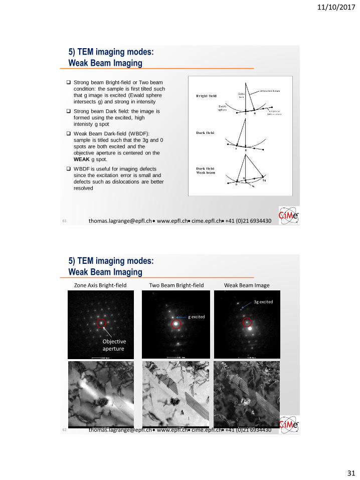
5) TEM imaging modes:
Weak Beam Imaging
Strong beam Bright-field or Two beam
condition: the sample is first tilted such
that g image is excited (Ewald sphere
intersects g) and strong in intensity
Strong beam Dark field: the image is
formed using the excited, high
intenisty g spot
Weak Beam Dark-field (WBDF):
sample is titled such that the 3g and 0
spots are both excited and the
objective aperture is centered on the
WEAK g spot.
WBDF is useful for imaging defects
since the excitation error is small and
defects such as dislocations are better
resolved
[email protected] www.epfl.ch cime.epfl.ch +41 (0)21 6934430 62
Weak Beam ImageTwo Beam Bright-fieldZone Axis Bright-field
5) TEM imaging modes:
Weak Beam Imaging
3g excited
g excited
Objective aperture

11/10/2017
32
[email protected] www.epfl.ch cime.epfl.ch +41 (0)21 6934430
5) TEM imaging modes:
Weak Beam Imaging
63
Weak Beam ImageTwo Beam Bright-field
Stripes spacing in the Stacking Fault correlate to partial dislocation separation
distances which can only be seen by weak beam dark-field imaging
[email protected] www.epfl.ch cime.epfl.ch +41 (0)21 6934430
Summary
TEM imaging modes
64
1. Mass-Thickness contrast
Applies for both crystalline and amorphous phase and scales with Z2t
2. Fresnel contrast
Developed by the interference of two waves, reference vacuum wave and one which scatters off the edges in the sample causing a path length difference and phase shift, resulting in fringe patterns that depend on the focus setting of the microscope
Can be used to correct objective astigmatism
3. Diffraction patterns
Can used to identify phase, orientation and crystal structure and these data can be correlated to the nanostructure features in the TEM image
Most calculate the camera constant (camera length for the TEM) in order to precisely index patterns
Simulations are needed to index lower symmetry crystals (non-cubic)
4. Diffraction contrast
Brightfield: objective aperture centered on “unscattered” beam (spot)
Dark-field: objective aperture centered on “diffracted beams (spot)
Weak Beam Dark-field: sample tilted to excited higher order “3g” reflections to higher intensity and objective aperture centered on low intensity “1g” spot
5. HR-TEM or Phase contrast
Developed by the interference of two waves, one which undergoes a phase shift due to the interactions with the sample crystal structure of a given thickness and is altered by the microscope aberrations
Simulations are needed to interpret phase contrast images properly
