intro to logic design 2 - homework for you
TRANSCRIPT
2 /100
CDA3201 Intro to Logic Design Lab Assignment
Name: Grade:
Dr. Petrie Lab 2, p. 1
Note: Each variable is one digit, the answer takes up 2 variables Cout and Sum. If you have more than 1 column of numbers, addition
is done from right to left. For the right most (least significant) column you only add 2 numbers, but for the rest of the columns you
add the 2 numbers shown in the column plus the carry from the column to its right. So to build an arithmetic unit that adds we will
need two types of components, one that adds 2 binary numbers, and one that adds 3:
Half Adder is used to add the least significant (right-most) column. It has 2 inputs: A,
and B; and 2 outputs (one for each digit in the answer). The least significant digit of the
answer is called Sum (written below the column), and the most significant digit of the
answer is called “carry” (Cout, written above the next column on left).
Full Adder to add each column other than the least significant column. It has 3 inputs:
the 2 numbers in the column: A, B, plus the carry Cout from the column to its right, now
called Cin. There are 2 outputs (one for each digit of the answer), the least significant
digit is the Sum, while the most significant is the carry out to the next column to its
left, which we call Cout.
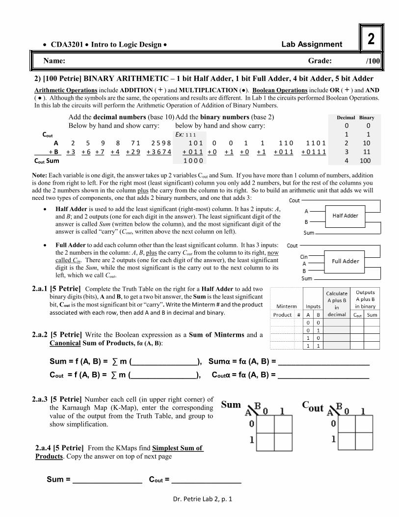
2.a.1 [5 Petrie] Complete the Truth Table on the right for a Half Adder to add two
binary digits (bits), A and B, to get a two bit answer, the Sum is the least significant
bit, Cout is the most significant bit or “carry”. Write the Minterm # and the product associated with each row, then add A and B in decimal and binary.
2.a.2 [5 Petrie] Write the Boolean expression as a Sum of Minterms and a
Canonical Sum of Products, fα (A, B):
Sum = f (A, B) = ∑ m (_______________), Sumα = fα (A, B) = _____________________
Cout = f (A, B) = ∑ m (_______________), Coutα = fα (A, B) = _____________________
2.a.3 [5 Petrie] Number each cell (in upper right corner) of
the Karnaugh Map (K-Map), enter the corresponding
value of the output from the Truth Table, and group to
show simplification.
2.a.4 [5 Petrie] From the KMaps find Simplest Sum of
Products. Copy the answer on top of next page
Sum = ________________ Cout = ________________
2) [100 Petrie] BINARY ARITHMETIC – 1 bit Half Adder, 1 bit Full Adder, 4 bit Adder, 5 bit Adder
Arithmetic Operations include ADDITION ( + ) and MULTIPLICATION (●). Boolean Operations include OR ( + ) and AND
( ● ). Although the symbols are the same, the operations and results are different. In Lab 1 the circuits performed Boolean Operations.
In this lab the circuits will perform the Arithmetic Operation of Addition of Binary Numbers.
Add the decimal numbers (base 10) Add the binary numbers (base 2) Decimal Binary
Below by hand and show carry: below by hand and show carry: 0 0 Cout Ex: 1 1 1 1 1 A 2 5 9 8 7 1 2 5 9 8 1 0 1 0 0 1 1 1 1 0 1 1 0 1 2 10 + B + 3 + 6 + 7 + 4 + 2 9 + 3 6 7 4 + 0 1 1 + 0 + 1 + 0 + 1 + 0 1 1 + 0 1 1 1 3 11 Cout Sum 1 0 0 0 4 100
2 /100
CDA3201 Intro to Logic Design Lab Assignment
Name: Grade:
Dr. Petrie Lab 2, p. 2
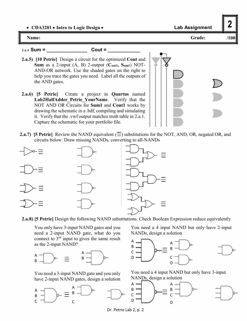
2.a.4 Sum = _______________ Cout = ____________
2.a.5) [10 Petrie] Design a circuit for the optimized Cout and
Sum as a 2-input (A, B) 2-output (Cout1, Sum1) NOT-
AND-OR network. Use the shaded gates on the right to
help you trace the gates you need. Label all the outputs of
the AND gates.
2.a.6) [5 Petrie] Create a project in Quartus named
Lab2HalfAdder_Petrie_YourName. Verify that the
NOT AND OR Circuits for Sum1 and Cout1 works by
drawing the schematic in a .bdf, compiling and simulating
it. Verify that the .vwf output matches truth table in 2.a.1.
Capture the schematic for your portfolio file.
2.a.7) [5 Petrie] Review the NAND equivalent ( ) substitutions for the NOT, AND, OR, negated OR, and
circuits below. Draw missing NANDs, converting to all-NANDs
2.a.8) [5 Petrie] Design the following NAND substitutions. Check Boolean Expression reduce equivalently
You only have 3-input NAND gates and you
need a 2-input NAND gate, what do you
connect to 3rd input to gives the same result
as the 2-input NAND?
You need a 3-input NAND gate and you only
have 2-input NAND gates, design a solution
You need a 4 input NAND but only have 2-input
NANDs, design a solution
You need a 4 input NAND but only have 3-input
NANDs, design a solution
A B C D A
B
AB
AB C
A B
C
A B
C D
A B C D
AB C
D
2 /20
CDA3201 Intro to Logic Design Lab Assignment
Name: Grade:
Dr. Petrie Lab 2, p. 3
2.a.9) [5 Petrie] Convert the simplified NOT-AND-OR circuit
in 2.a.5 to an all-NAND gates. Make sure to remove
these pair of extra NANDs to make the Simplest all
NAND circuit. Label outputs Cout2, Sum2 Note: when
you do the substitution that sometimes you end up with two “NOTs” in a row
along the same wire. This “NOT” pair can be removed because they cancel:
(A’)’ = A. You may want to draw it on scratch paper before transferring your
design to the diagram on the right
2.a.10) [5 Petrie] Open the 2.a.6 Quartus project. Add to
the .bdf file the schematics of the Cout2 and Sum2
of all-NAND circuits. Compile, simulate, and
verify 2.a.5 and 2.a.7 circuits are equivalent.
Capture the all-NAND schematic and .vwf results
for portfolio.
2.a.11) [10 Petrie] Once verified equivalent, plan your wiring below of both circuits but DO NOT WIRE
on the breadboard. Label all inputs and outputs of the gates used. Note: wires from gray/green tube in kit contains four twisted-
pairs of wires: BROWN and Brown/White, ORANGE and Orange/White, GREEN and Green/White, BLUE and Blue/White. These
can be used for up to 4 inputs that can be noted. Note: you have other colors that have no corresponding white striped wire: WHITE,
GREY, PURPLE, YELLOW, besides these: RED used for Vcc (Power), and BLACK used for Ground (avoid using these in your
circuit except for these uses). Use a different colored solid wire for each input, and corresponding color/White for corresponding NOT
(use dashed lines and color below to plan the use of wires).
Suggested
color code
Inputs:
BLUE GREEN BROWN ORANGE
In-Between:
WHITE
YELLOW
Outputs:
GREY
PURPLE
Vcc and GND:
RED
BLACK
Cout Sum
Cout2 Sum2

2 /100
CDA3201 Intro to Logic Design Lab Assignment
Name: Grade:
Dr. Petrie Lab 2, p. 4
2.a.12 [10 Petrie] By abstracting our design for the Half Adder into a “black box”, hiding all the gates
of the circuit (does not matter if NOT-AND-OR or all-NAND), we can use it as a component to
simplify how to design more complex components. Use Half Adders as
components to build a Full Adder. A Full Adder adds 3 inputs: Carry-in (Cin)
plus the two input bits: A and B. A Half Adder can only add 2 at a time, so we
need multiple Half Adders. Figure out how many Half Adders below are
needed and connect them to get the Cout and Sum answer of a Full Adder.
2.a.13 [5 Petrie] Complete the truth table for a Full Binary Adder. There are 3 inputs: A and B, and the carry
from previous stage, called Cin. Label the sum bit is Sum3 and the carry to next stage is Cout3.
Inputs A B Cin
Calculate sum of A, B, Cin in
decimal
Outputs in binary
Cout3 Sum3 0 0 0
0 0 1
0 1 0
0 1 1
1 0 0
1 0 1
1 1 0
1 1 1
2.a) [2 Petrie] From the Truth Table,write the Sum of Minterms and the Canonical Sum of Products:
Sum3 = f (A, B, Cin) = ∑ m (_____________), Sum3α = __________________________
Cout3 = f (A, B, Cin) = ∑ m (_____________), Cout3α = __________________________
2.b) [2 Petrie] Optimize the above functions using K-
maps, label each cell with the corresponding minterm
number in the upper right of each cell, then fill in the
values of each cell according to the Truth table, find
the groupings and the simplest Sum of Products:
Sum3 = f (A, B, Cin) = __________________
Cout3 = f (A, B, Cin) = __________________
2 /100
CDA3201 Intro to Logic Design Lab Assignment
Name: Grade:
Dr. Petrie Lab 2, p. 5
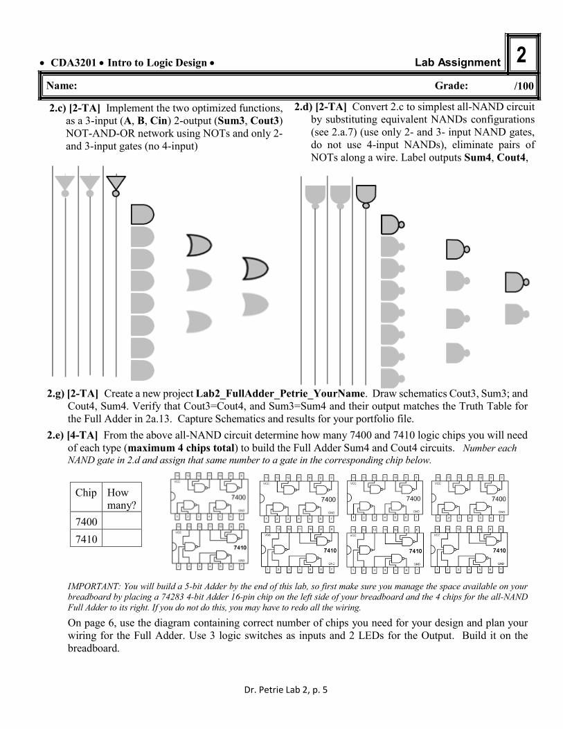
2.c) [2-TA] Implement the two optimized functions,
as a 3-input (A, B, Cin) 2-output (Sum3, Cout3)
NOT-AND-OR network using NOTs and only 2-
and 3-input gates (no 4-input)
2.d) [2-TA] Convert 2.c to simplest all-NAND circuit
by substituting equivalent NANDs configurations
(see 2.a.7) (use only 2- and 3- input NAND gates,
do not use 4-input NANDs), eliminate pairs of
NOTs along a wire. Label outputs Sum4, Cout4,
2.g) [2-TA] Create a new project Lab2_FullAdder_Petrie_YourName. Draw schematics Cout3, Sum3; and
Cout4, Sum4. Verify that Cout3=Cout4, and Sum3=Sum4 and their output matches the Truth Table for
the Full Adder in 2a.13. Capture Schematics and results for your portfolio file.
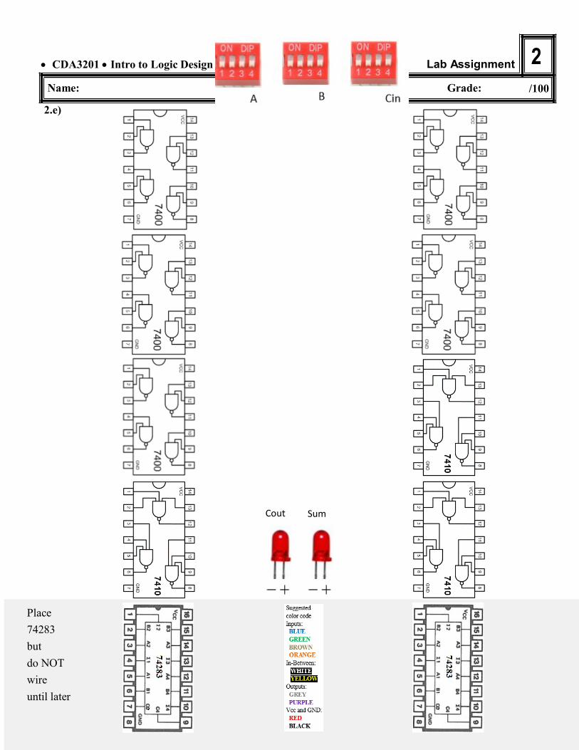
2.e) [4-TA] From the above all-NAND circuit determine how many 7400 and 7410 logic chips you will need
of each type (maximum 4 chips total) to build the Full Adder Sum4 and Cout4 circuits. Number each
NAND gate in 2.d and assign that same number to a gate in the corresponding chip below.
Chip How
many?
7400
7410
IMPORTANT: You will build a 5-bit Adder by the end of this lab, so first make sure you manage the space available on your
breadboard by placing a 74283 4-bit Adder 16-pin chip on the left side of your breadboard and the 4 chips for the all-NAND
Full Adder to its right. If you do not do this, you may have to redo all the wiring.
On page 6, use the diagram containing correct number of chips you need for your design and plan your
wiring for the Full Adder. Use 3 logic switches as inputs and 2 LEDs for the Output. Build it on the
breadboard.
2 /100
CDA3201 Intro to Logic Design Lab Assignment
Name: Grade:
Dr. Petrie Lab 2, p. 6
2.e)
Place
74283
but
do NOT
wire
until later
Cout Sum
2 /100
CDA3201 Intro to Logic Design Lab Assignment
Name: Grade:
Dr. Petrie Lab 2, p. 7
As you see there are many connections to create a 1 bit adder. Now we abstract
all those gates into a “black box” as shown at right. We will use the black box as
a component to build other things, only worrying about the inputs and outputs and
how to interconnect the components, not what
is inside the box.
Below we see how we can connect four 1-bit Full Adders to create a 4-bit adder.
Note instead of A and B the inputs are a 4-bit number: A4 A3 A2 A1 and another
4-bit number B4 B3 B2 B1 and a 1 bit Cin, and the outputs, Cout remains 1 bit but
instead of Sum is a 4-bit S4 S3 S2 S1.
We can abstract the 4-bit adder we built above into one “black box”, which turns out to be packaged into
the 74283 chip. Below we see the logical diagram vs pinout diagram of the 74283. Note from the pinouts
of the 74283, C0 is equivalent to Cin, C4 is equivalent to Cout, and ∑ is S (Sum).
How do we connect four 74283 4-bit adders to make a 16-bit adder? (Hint: see connections of four 1-bit
adders above to make a 4-bit adder above)
Sum
FULL
ADDER
Cout
A B Cin
2 /100
CDA3201 Intro to Logic Design Lab Assignment
Name: Grade:
Dr. Petrie Lab 2, p. 8
Sum
A B
FULL
ADDER Cout
Cin
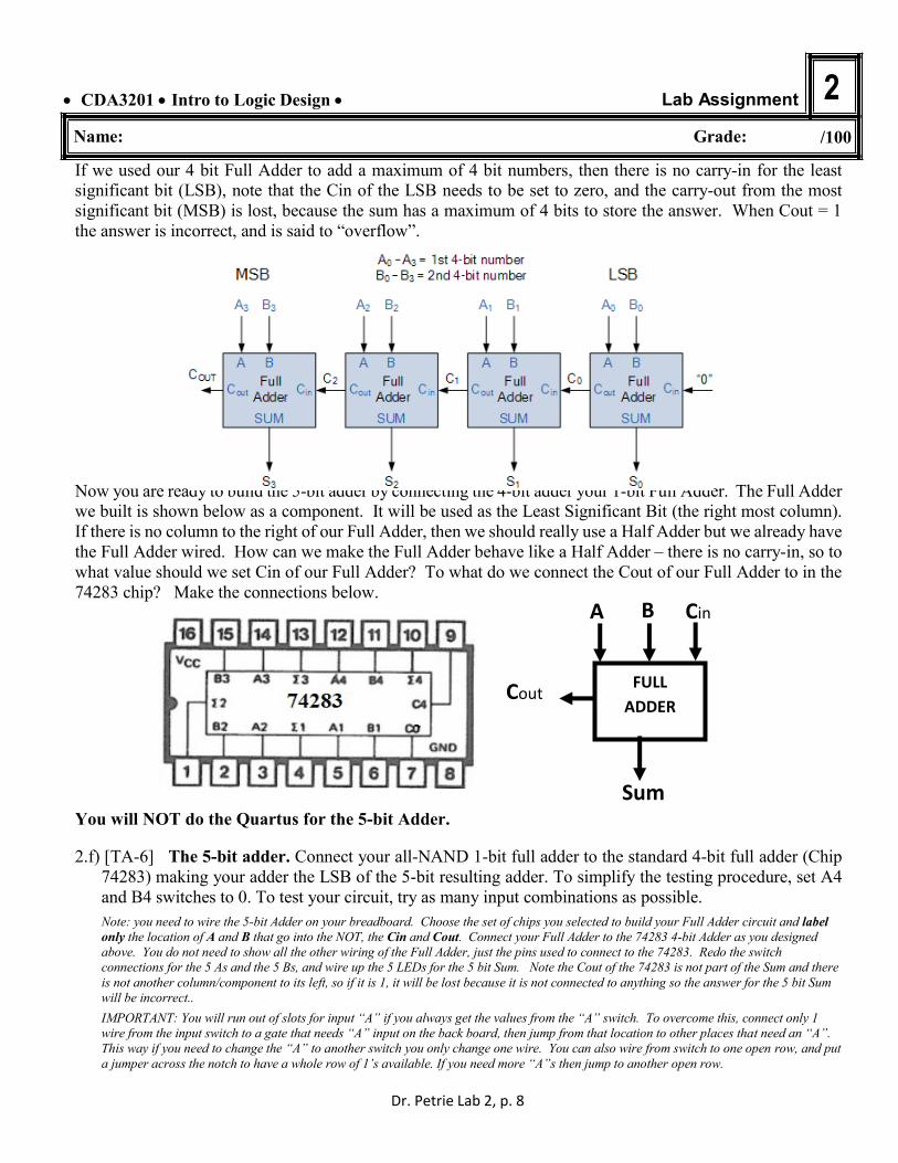
If we used our 4 bit Full Adder to add a maximum of 4 bit numbers, then there is no carry-in for the least
significant bit (LSB), note that the Cin of the LSB needs to be set to zero, and the carry-out from the most
significant bit (MSB) is lost, because the sum has a maximum of 4 bits to store the answer. When Cout = 1
the answer is incorrect, and is said to “overflow”.
Now you are ready to build the 5-bit adder by connecting the 4-bit adder your 1-bit Full Adder. The Full Adder
we built is shown below as a component. It will be used as the Least Significant Bit (the right most column).
If there is no column to the right of our Full Adder, then we should really use a Half Adder but we already have
the Full Adder wired. How can we make the Full Adder behave like a Half Adder – there is no carry-in, so to
what value should we set Cin of our Full Adder? To what do we connect the Cout of our Full Adder to in the
74283 chip? Make the connections below.
You will NOT do the Quartus for the 5-bit Adder.
2.f) [TA-6] The 5-bit adder. Connect your all-NAND 1-bit full adder to the standard 4-bit full adder (Chip
74283) making your adder the LSB of the 5-bit resulting adder. To simplify the testing procedure, set A4
and B4 switches to 0. To test your circuit, try as many input combinations as possible.
Note: you need to wire the 5-bit Adder on your breadboard. Choose the set of chips you selected to build your Full Adder circuit and label
only the location of A and B that go into the NOT, the Cin and Cout. Connect your Full Adder to the 74283 4-bit Adder as you designed
above. You do not need to show all the other wiring of the Full Adder, just the pins used to connect to the 74283. Redo the switch
connections for the 5 As and the 5 Bs, and wire up the 5 LEDs for the 5 bit Sum. Note the Cout of the 74283 is not part of the Sum and there
is not another column/component to its left, so if it is 1, it will be lost because it is not connected to anything so the answer for the 5 bit Sum
will be incorrect..
IMPORTANT: You will run out of slots for input “A” if you always get the values from the “A” switch. To overcome this, connect only 1
wire from the input switch to a gate that needs “A” input on the back board, then jump from that location to other places that need an “A”.
This way if you need to change the “A” to another switch you only change one wire. You can also wire from switch to one open row, and put
a jumper across the notch to have a whole row of 1’s available. If you need more “A”s then jump to another open row.

2 /100
CDA3201 Intro to Logic Design Lab Assignment
Name: Grade:
Dr. Petrie Lab 2, p. 9
2.f)
∑1 ∑4 ∑3 ∑2 ∑0
2 /100
CDA3201 Intro to Logic Design Lab Assignment
Name: Grade:
Dr. Petrie Lab 2, p. 10
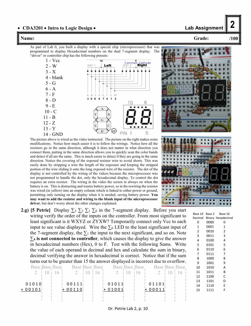
As part of Lab 0, you built a display with a special chip (microprocessor) that was
programmed to display Hexadecimal numbers on the dual 7-segment display. The
“driver” or controller chip has the following pinouts:
1 - Vcc
2 - W
3 - X
4 - blank
5 - G
6 - A
7 - F
8 - D
9 - E
10 - C
11 - B
12 - Z
13 - Y
14 - GND The picture above is wired as the video instructed. The picture on the right makes some
modifications. Notice how much easier it is to follow the wirings. Notice how all the
resistors go in the same direction, although it does not matter in what direction you
connect them, putting in the same direction allows you to quickly scan the color bands
and detect if all are the same. This is much easier to detect if they are going in the same
direction. Notice the covering of the exposed resistor wire to avoid shorts. This was
easily done by stripping a wire the length of the exposure and keeping the stripped
portion of the wire sliding it onto the long exposed wire of the resistor. The dot of the
display is not controlled by the wiring of the videos because the microprocessor was
not programmed to handle the dot, only the hexadecimal display. To control the dot
requires an extra resistor. The wiring in the video the screen in always on when the
battery is on. This is distracting and wastes battery power, so in the rewiring the resistor
was wired (in yellow) into an empty column which is linked to either power or ground,
permitting only turning on the display when it is needed, saving battery power. You
may want to add the resistor and wiring to the blank input of the microprocessor
driver, but don’t worry about the other changes explained.
2.g) [5 Petrie] Display ∑3 ∑2 ∑1 ∑0 in the 7-segment display. Before you start
wiring verify the order of the inputs on the controller. From most significant to
least significant is it WXYZ or ZYXW? Temporarily connect only Vcc to each
input to see value displayed. Wire the ∑0 LED to the least significant input of
the 7-segment display, the ∑1 the input to the next significant, and so on. Note
∑4 is not connected to controller, which causes the display to give the answer
in hexadecimal numbers (Hex), 0 to F. Test with the following Sums. Write
the value of each operand in decimal and hex and calculate the sum in binary,
decimal verifying the answer in hexadecimal is correct. Notice that if the sum
turns out to be greater than 15 the answer displayed is incorrect due to overflow.
Base Base Base Base Base Base Base Base Base Base Base Base
2 10 16 2 10 16 2 10 16 2 10 16
0 1 0 1 0 0 0 1 1 1 0 1 0 1 1 0 1 1 0 1 + 0 0 1 0 1 + 0 0 1 1 0 + 0 1 0 0 1 + 0 0 0 1 1
Base 16 Hexadecimal
0 1 2 3 4 5 6 7 8 9 A B C D E F
Base 2 Binary
0000 0001 0010 0011 0100 0101 0110 0111 1000 1001 1010 1011 1100 1101 1110 1111
Base 10 Decimal
0 1 2 3 4 5 6 7 8 9
10 11 12 13 14 15