international technology roadmap for photovoltaic … downloads/itrpv_2014_road… · international...
TRANSCRIPT

International TechnologyRoadmap for Photovoltaic (ITRPV)
2013 Results
International Technology Roadmap for Photovoltaic
FifthEditionMarch 2014
Supported by:

2
AcknowledgementList of Authors (in alphabetical order by company)Hali Forstner, Sandeep Bandil; Applied MaterialsMartijn Zwegers; BE Semiconductor Industries
Roel Bollen; Ducatt NVGianluca Coletti, Wim Sinke, Jan Bultman, Paul
Wyers; ECN Solar EnergyRoland Wertz; Fraunhofer IPAStone Wu; GD SolarKC Lin; Gintech Energy CorporationAxel Metz*; Moritz Meixner; h.a.l.m. elektronikMarkus Fischer*, Thomas Spiess, Michael
Mette, Ansgar Mette, Kai Petter, Alexander
Gerlach, Peter Engelhart; Hanwha Q-CellsGuoqiang Xing*; Hareon SolarAndrey Demenik; Helios ElectroDavid McMullen, Carsten Mohr, Arno Stassen;
Heraeus Precious Metals (PV Business Unit)Jozef Slufcik; imecLiu Yong*; JA SolarStefan Kaufmann; Komax Solar
Yuepeng Wan; LDK SolarYingge Wang, Sophie Liu; LONGi SiliconAndré Richter; Meyer BurgerRichard Pai, Kirin Wang; Motech IndustriesBob Chen, Andy Luan; Neo Solar Power CorporationIryna Buchovskaja; Pillar Ltd. Burkhard Spill, Roger Pingel; PVA TePlaArun Ramakrishnan; RCT Solutions Stein Julsrud*, Wayne Osborne, Archie Flores;
REC SiliconPeter Fath, Hartmut Nussbaumer; RENAStephan Raithel; SEMISebastian Pingel, Oliver Frank; SOLONJim Zhu; Suntech PowerAlan Ristow, Lars Oberbeck; TOTAL New EnergyGrigory Demenik; Technology K
* Co-chair of the ITRPV working group
h.a.l.m. develops and delivers high-end measuring systems for photovoltaic technologies worldwide. For further information visit www.halm.de
SEMI promotes the development of the global micro and nano-manufacturing supply chain and positively influences the growth and prosperity of its members. SEMI advances the mutual business interests of its membership and promotes fair competition in an open global marketplace.
VDMA Photovoltaics Equipment delivers key services to the photovoltaic equipment industry in Germany.
Industry Supporters
www.itrpv.net 3
Table of Contents1. Executive summary 4
2. Approach 5
2.1 Materials 5
2.2 Processes 5
2.3 Products 5
3. PV learning curve and cost reduction 7
4. Cost considerations 8
5. 2013 Results 10
5.1 Materials _______________________________________________ 10
5.1.1 Materials – crystallization and wafering 10
5.1.2 Materials – cell processing 12
5.1.3 Materials – modules 15
5.2 Processes ______________________________________________ 17
5.2.1 Processes – manufacturing __________________________ 17
5.2.2 Processes – technology _____________________________ 22
5.3 Products _______________________________________________ 27
6. PV Systems 32
7. Outlook 34
8. References 36

4
1. Executive summaryThe photovoltaic (PV) industry has to provide power generation products that are competitive with conventional and other renewable sources of energy. An international technology roadmap helps to identify trends and define requirements for necessary improvements. The aim of the SEMI International Technology Roadmap for Photovoltaic (ITRPV) is to inform suppliers and customers about expected technology trends in the field of crystalline silicon (c-Si) photovoltaic and to add to discussions on required improvements and standards. The objective of the roadmap is not to recommend detailed technical solutions for identified areas of improvement, but to emphasize to the PV community the need for improvement and to encourage comprehensive solutions to be found. The present, fifth edition of the ITRPV was jointly prepared by 28 leading international c-Si solar cell manufacturers, module manufacturers, silicon producers, wafer suppliers, PV equipment suppliers and production material providers, as well as PV research institutes. The present publication covers the entire PV value chain from crystallization, wafering and cell manufacturing to module manufacturing and PV systems. Significant parameters set out in earlier editions are reviewed along with some new ones, and discussions about emerging trends in the PV industry are reported.The global PV module production capacity in 2014 is assumed to be approximately 62.7 GW (c-Si: 56.6 GW; thin film: 6.1 GW; the c-Si market has a market share of 90% while the thin-film market has 10%) [0]. Technological developments and trends for c-Si module production capacity are described in this roadmap. The costs of ownership for c-Si crystallization, wafering, cell and module manufacturing revealed that despite prices having stabilized since the summer of 2013, the industry focus remains on reducing the costs per Watt peak (Wp) by improving the efficiency of all resources, materials and consumables, including silicon, as well as by introducing new technologies to increase module output power. New technologies have to be implemented without significantly increasing costs per unit, despite the necessarily more complex manufacturing processes involved. A historic learning rate of above 20% can be maintained over the next few years by introducing new double- and single-sided contact cell concepts with improved Si-wafers, as well as improved cell fronts and rear sides and better module technologies. This will result in standard multi-crystalline silicon (mc-Si) modules with an average output power of above 290 Wp (60-cell modules) by 2024. The combination of increased cell and module performance in conjunction with significantly reduced manufacturing costs will support the reduction of PV system costs and thus ensure the long-term competitiveness of PV power generation.
This roadmap activity will be continued in cooperation with SEMI, and updated information will be published in the spring of each year to ensure good communication between manufacturers and suppliers across the value chain. More information is available at www.itrpv.net.

www.itrpv.net 5
2. ApproachAll topics along the value chain were divided into three areas: materials, processes and products. Data values were collected from the participating companies and were processed anonymously by SEMI. All companies jointly agreed to the results being reported in this roadmap publication. Color marking, as shown in Table 1, is used to describe the maturity of a technology according to different parameters: green indicates that the technology is in use, yellow means that an industrial solution is known but is not yet used in mass production, orange means that an interim solution exists, but it is too expensive, while red indicates that there is no known industrial solution available. All parameters are median values based on data from recent production line output.As stated above, the topics are split into three areas: materials, processes and products. We address issues connected with crystallization, wafers, cells, modules and PV systems for each of these areas respectively.
Green Industrial solution exists, and is being optimized in production
Yellow Industrial solution is known but not yet in mass production
Orange Interim solution is known, but too expensive or not suitable for production
Red Industrial solution is not known
Table 1 Color marking to visualize the maturity of technologies.
2.1 MaterialsThe requirements and trends concerning raw materials and consumables used within the value chain are described in this section. Replacing some materials will be necessary in order to secure availability, avoid environmental risks, reduce costs and increase efficiency. Price development plays a major role in making PV-generated electricity competitive with other renewable sources of energy.
2.2 ProcessesNew technologies, materials and highly productive manufacturing equipment are required to reduce production costs. By providing information on key production figures, as well as details about processes designed to increase cell efficiency and the power output of modules, this roadmap constitutes a guide to new developments with the aim of supporting their progress. The section on processes identifies manufacturing and technology issues for each part of the value chain. Manufacturing topics center on increased productivity while technological developments aim at ensuring higher cell and module efficiencies.
2.3 ProductsEach part of the value chain has a final product. The product section therefore discusses the development of key elements such as ingots, wafers, c-Si solar cells, and modules and PV systems over the coming years.

6
The ITRPV is updated using information provided by manufacturers, R&D institutes and equipment and material suppliers. Furthermore, the contributors not only represent the whole manufacturing supply chain but also equally represent the relevant regions for PV manufacturing.
Fig. 0 ITRPV contributors by affiliation to PV value chain.
33%
11%
55%SuppliersR&D InstitutesManufacturers

www.itrpv.net 7
3. PV learning curve and cost reductionIt is obvious that cost reductions in PV production processes have to result in price reductions [1]. Fig. 1 shows the price experience curve for PV modules, displaying the average module sales price (in USD/Wp for 2011) as a function of cumulative module shipments from 1976 to 12/2013 (in MWp) [2]. Module shipments have been ahead of PV system installations for years [3]. Displayed on a log-log scale, the plot is approximately linear until the shipment value of 3.1 GWp (representing shipments at the end of 2003) despite kinks at around 100 MWp. This indicates that for every doubling of cumulative PV module shipments, the average selling price decreases with a learning rate (LR) of about 21%. The large deviations from the LR plot in Fig.1 are caused by tremendous market fluctuations that have taken place since 2003. The first point below 1 USD/Wp indicates the average module price at the end of 2011 of 0.95 USD/Wp with over 77 GWp shipped. Enormous oversupply between 2011 and 2012 caused a significant price drop to 0.69 USD/Wp at the cumulated shipment of 110 GWp. The last data point considers the estimated shipment volume in 2013 of about 39 GWp [3], [4] at the price of 0.72 USD/Wp [2]. The 100 GWp landmark was therefore clearly exceeded in 2012 [5] and the current cumulated shipped module power is approximately 149 GWp.
Fig.1 Learning curve for module price as a function of cumulative PV module shipments.
ITRPV 2014
10 -1 10 0 10 1 10 2 10 3 10 4 10 5 10 6 10 70,1
1
10
100
10 -1 10 0 10 1 10 2 10 3 10 4 10 5 10 6 10 7
0,1
1
10
100
aver
age
mod
ule
sale
s pric
e (U
SD 2
011/
Wp)
cumulative PV module shipments (MWp)
historic data LR 21,5%

8
4. Cost considerationsFig. 2 shows the price development of mc-Si modules from January 2010 to January 2014 with separate price trends for poly-Si, multi crystalline (mc) wafers and cells respectively [6]. The price erosion in 2011/2012 was mainly caused by huge oversupply along the PV value chain, resulting in prices that were even below the production cost of c-Si modules [7]. The current module price level appears to be stable and sustainable, with a 28% PV market growth in 2013 (approximately 39 GW) compared to 2012 [8]. The average poly-Si price was approximately 20 USD/kg in January 2014 [6]. This indicates that the poly-Si price drop has halted due to upcoming demand, and prices have even increased slightly compared to January 2013. 20 USD/kg represented the total level of costs for top tier suppliers in 2012 [9]. This resulted in changes to the different cost elements in module production. This is a drawback for module manufacturing as it has increased pressure to find further cost reductions.
Fig. 3 shows the proportion of costs attributable to silicon, wafer, cell, and module costs. The overall price level did not change significantly from 01/2013 to 01/2014 but the share of different cost elements shifted slightly. Increased cell costs were not fully transferred to the module price.
0.0
0.2
0.4
0.6
0.8
1.0
1.2
1.4
1.6
1.8
2.0
Avar
age
Multi
Mod
ule
Pric
es (U
SD/W
p)
Silicon Multi Wafer Multi Cell Multi Module
ITRPV 2014
Fig. 2 Price trends for poly-Si, mc-Si wafers, cells and c-Si modules (Assumption: 44.1 Wafers per kg with ~22.7g/wafer, average mc-Si cell efficiency 17.3% (4.21 Wp) [6].

www.itrpv.net 9
Non-silicon module manufacturing costs are mainly driven by consumables and materials, as discussed in the c-Si PV module cost analysis in the third edition of the ITRPV. Taking into account that the expected global PV module production capacity in 2014 of >62.7 GW [4] will still slightly exceed the global market demand of about 45-55 GW, prices will not compensate for cost increases. Driving cost reductions in consumables and materials will therefore remain a major task for the industry.
Three strategies will help meet this challenge:
i) Continue to reduce costs per unit along the whole value chain by optimizing usage of installed production capacity and by the efficient use of Si and non-Si materials, ii) Introduce specialized module products for different market applications (i.e. balance cost- optimized high-volume products with fully customized niche products), and iii) Improve module power/cell efficiencies without significantly increasing processing costs.
The latter implies that improvements in efficiency have to be implemented using lean processes, requiring minimum investments in new tool sets in order to avoid a significant increase in depreciation costs.
Poly Si 17% Poly Si 13% Poly Si 15%
Wafer 25%Wafer 16% Wafer 17%
Cell 25%
Cell 22% Cell 23%
Module 33%Module 49% Module 44%
Share 01/2010 Share 01/2013 Share 01/2014
ITRP
V 20
14
Fig. 3 Comparison of the proportion of price attributable to different module cost elements between 01/2010, 01/2013 and 01/2014 (1.86, 0.69, and 0.72 $/W).

10
5. 2013 Results5.1 Materials
5.1.1 Materials – crystallization and waferingPoly-Si production technologies show a potential for improvement, as discussed in Section 3. We expect FBR technology to increase its share against Siemens processing, as shown in Fig. 4. Other technologies such as umg-Si are not predicted to yield significant cost advantages compared to conventional poly-Si technologies over the coming years.
Discussions with producers have revealed that major poly-Si quality reductions do not lead to significant cost reductions. Despite the possibility of using 6N material for p-type mc-Si cells, its application would not result in cost reductions as the price is not significantly lower than that of 9N [9]. We foresee that a PV-grade poly-Si quality of between 8N and 9N will be sufficient for current and future p- and n-type cell concepts, another reason for this being the fact that feedstock purity is not the sole variable affecting wafer quality.
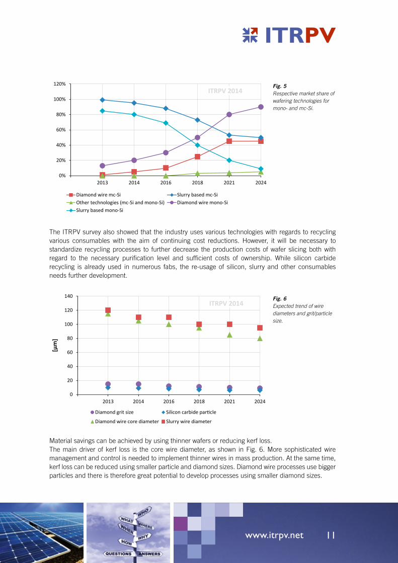
A significant improvement in cost reductions in the wafering process is expected due to the introduction of diamond wire sawing, especially for mono wafers. Diamond wire sawing is expected to become widespread for mono-Si wafering; however, the field is open with regard to mc-Si wafering. Other new wafer manufacturing techniques, especially kerf-less technologies, are not expected to gain notable market shares due to the maturity of the established sawing technologies. Fig. 5 shows the expected share of wafering technologies in volume production. The roll out of diamond wire sawing technology requires synchronization with cell process development.
0%
10%
20%
30%
40%
50%
60%
70%
80%
90%
2013 2014 2016 2018 2021 2024
Share of Siemens Process Share of FBR Process Share of other
ITRPV 2014Fig. 4 Expected change in share of poly-Si production technologies.
www.itrpv.net 11
The ITRPV survey also showed that the industry uses various technologies with regards to recycling various consumables with the aim of continuing cost reductions. However, it will be necessary to standardize recycling processes to further decrease the production costs of wafer slicing both with regard to the necessary purification level and sufficient costs of ownership. While silicon carbide recycling is already used in numerous fabs, the re-usage of silicon, slurry and other consumables needs further development.
Material savings can be achieved by using thinner wafers or reducing kerf loss.The main driver of kerf loss is the core wire diameter, as shown in Fig. 6. More sophisticated wire management and control is needed to implement thinner wires in mass production. At the same time, kerf loss can be reduced using smaller particle and diamond sizes. Diamond wire processes use bigger particles and there is therefore great potential to develop processes using smaller diamond sizes.
0%
20%
40%
60%
80%
100%
120%
2013 2014 2016 2018 2021 2024
Diamond wire mc-Si Slurry based mc-SiOther technologies (mc-Si and mono-Si) Diamond wire mono-SiSlurry based mono-Si
ITRPV 2014Fig. 5 Respective market share of wafering technologies for mono- and mc-Si.
Fig. 6 Expected trend of wire diameters and grit/particle size.
0
20
40
60
80
100
120
140
2013 2014 2016 2018 2021 2024
[µm
]
Diamond grit size Silicon carbide particle
Diamond wire core diameter Slurry wire diameter
ITRPV 2014

12
If we take into consideration all factors in kerf losses (wire core diameter, grit size and sub-surface damage), the overall kerf-loss reduction potential is higher for diamond wire processes, as shown in Fig. 19.
Consumables such as crucibles, graphite parts, slurry and sawing wires provide opportunities for cost reduction in crystallization and wafering. We foresee that prices will also be affected by the cost of these goods and price reductions of between 5% and 10% per year, as shown in Fig. 7, seem possible.The increasing share of diamond wiring means that the price level of diamond wires will need to reach 25% of today’s price by 2023.
5.1.2 Materials – cell processingThe Si wafers account for approximately 57% of the cell price today, as shown in Fig. 3. Reducing the as-cut wafer thickness would result in a more efficient use of silicon. Wafer thickness reduction has the following technological implications:
i) improved wafer sawing technologies + reduced kerf loss and Total Thickness Variation (TTV), ii) innovative handling concepts, iii) new high eta cell concepts suitable for thinner wafers, iv) new interconnect and encapsulation technologies at module level.
Wafer and cell manufacturers would like to reduce the thickness of wafers to cut costs. Fig. 8 shows the expected trend of mass-produced thin as-cut wafers. Former roadmaps have not materialized as predicted due to lower market prices for wafers. Instead of using thinner wafers to reduce production costs, cost-effective thicker wafers were used, thereby reducing the breakage on production lines. The pressure to use thinner wafers to further decrease costs will increase due to the expected tight wafer market situation [3]. Fig. 8 also shows the cell thickness limits of current module technologies, with tool suppliers and R&D institutes predicting a more pronounced reduction for alternative interconnection
Fig. 7 Expected relative price reductions for key consumables in crystallization and wafering (2013 = 100%).
65%
70%
75%
80%
85%
90%
95%
100%
105%
2013 2014 2016 2018 2021 2024
CZ graphite parts CZ crucibles Casting graphite parts Casting crucibles
ITRPV 2014

www.itrpv.net 13
technologies, e.g. for rear-side contact cells. The wafer thickness requirements of cell producers will meet the targets of wafer suppliers until 2017/2018. Following that, reductions will continue but the rate at which this happens shall depend on the material and technology (e.g. PERC) used. R&D institutes and tool manufacturers are making preparations to be ahead of industry demands. Wafers in the current standard format (156x156 mm²) will remain standard until 2023; larger wafers (210x210 mm²) are not expected to appear in production in the near future.
Metallization pastes/inks containing silver (Ag) and aluminium (Al) are the most process-critical and expensive materials used in current cell technologies aside from the wafer itself. Paste consumption therefore needs to be reduced. Fig. 9 shows our estimations for reducing the silver that remains on a 156x156 mm² cell after processing. Compared to the last edition of the ITRPV, reductions have increased substantially and only 100 mg is deposited on cells today. New developments in pastes and screens enabled this reduction, which clearly shows the reaction of suppliers to the needs of cell manufacturers. The average price of silver of 690 USD/kg in February 2014 resulted in costs of 7 USD/cell (0.0167 USD/Wp), or about 10% of the non-Si cell price, as shown in Fig. 2. This is one third of the assumed total costs for last year. Because the price of silver is expected to remain high, following the recommendations laid out in this roadmap for reducing silver consumption is therefore mandatory if further cost reductions are to be achieved.
Fig. 8Predicted trend for minimum as-cut wafer thickness in mass production of solar cells and minimum cell thickness in module manufacturing.
0
25
50
75
100
125
150
175
200
225
2013 2014 2016 2018 2021 2024
[µm
]
Avg. wafer thickness multi + monoMinimum wafer thicknessMaximum wafer thicknessLimit of cell thickness in current module technologyLimit of cell thickness in alternative module technology
ITRPV 2014

14
As an alternative to the reduction of silver consumption at the cell manufacturing level, silver should be replaced on a large-scale basis by a more cost-effective material. Copper (Cu) is the intended substitute. The expected introduction of Cu into mass production is not expected to start before 2018 in any significant volume. This delay with respect to the assumptions of the fourth edition of the ITRPV is mainly due to the lack of progress in screen printing. Before the introduction of alternative metallization techniques, technical issues in reliability and adhesion have to be resolved. Appropriate equipment and processes also need to be available. Screen printing will remain a widespread metallization technology. Plating technologies are expected to obtain a wider share in metallization technologies in the long run, as shown in Fig. 9.
Pastes containing lead are restricted according to legislation that came into force in 2011 under the EU Directive on the Restriction of Use of Hazardous Substances (RoHS 2). This restriction affects the use of lead and other substances in electric and electronic equipment (EEE) on the EU market. It also applies to components used in equipment that fall within the scope of the Directive. PV panels are excluded from RoHS 2, meaning that they can contain lead and do not have to comply with the maximum weight concentration thresholds set out in the Directive.1 PV’s exclusion from the Directive will remain in force for the next few years – a review of RoHS 2 should take place by mid-2021 at the latest.2 Cell manufacturers should tread carefully, however: the exclusion in question is limited to PV panels installed in a defined location for permanent use (i.e. power plants, rooftops, building integration etc). Should the component in question also be useable in other equipment that is not excluded from RoHS 2, e.g. to charge calculators, then the component must comply with the Directive’s provisions.
1 Article 2(i) of the RoHS Directive [2011/65/EU] excludes “photovoltaic panels intended to be used in a system that is designed, assembled and installed by professionals for permanent use at a defined location to produce energy from solar light for public, commercial, industrial and residential applications” from the scope of the Directive.2 Article 24 of the RoHS Directive [2011/65/EU] requires an evaluation and possible revision of the Directive, including its scope, by 22 July 2021.
Fig. 9Proportion of silver per cell (156x156 mm²) and the predicted share of different metallization technologies in the cell process. (Color coding refers to silver reduction).
0%
10%
20%
30%
40%
50%
60%
70%
80%
90%
100%
0.000
0.020
0.040
0.060
0.080
0.100
0.120
0.140
0.160
2013 2014 2016 2018 2021 2024
[g/c
ell]
Silver per cell Plating in production
ITRPV 2014

www.itrpv.net 15
5.1.3 Materials – modulesModule add-on costs are heavily influenced today by material costs. Both improvements in module performance, as shown in section 5.3, as well as reductions in material costs, are required to reduce module add-on costs. Approaches to improve performance include the reduction of optical losses, e.g. the absorption and reflection of front cover glass and the reduction of interconnector losses. Approaches for reducing material costs include:
i) reducing material volume, e.g. material thickness, ii) replacing expensive materials, iii) reducing waste material.
To improve the transmission of the front cover glass, the use of antireflective- (AR-) coated or surface-structured glass has become common in recent years. Increasing the transmission over the relevant range of the solar spectrum requires further optimization of antireflective coatings and glass surface structures matched to module applications and the material used (e.g. solar cells). Increases in module performance by up to 2% can be expected, as shown in Fig. 10.
Furthermore, the transmission of encapsulant materials in the UV-range of the spectrum can be significantly improved by shifting the UV cut-off to lower wavelengths in order to use the improved blue response of advanced cell structures (e.g. low-doped and selective emitters) effectively.
Fig. 11 shows the trend for reducing the thickness of the front-side glass, encapsulant and backsheet. Reducing the thickness of glass to 2 mm requires new solutions for mechanical stabilization if used in a single glass module design. However, if used in a double glass module, even two 2 mm thin glass sheets should provide sufficient mechanical stability to avoid the use of additional stabilization
Fig. 10Effective transmission of front cover glass for PV-modules.
92.5%
93.0%
93.5%
94.0%
94.5%
95.0%
95.5%
96.0%
2013 2014 2016 2018 2021 2024
Transmission of glass

16
structures. In recent years the industry has made significant progress in both cost-effectively producing hardened glass with a thickness even below 2.5 mm and making this product available on the market.
Identified consumables in module production such as frames, backsheets, encapsulants, interconnectors and junction boxes have contributed more or less equally to the distribution of costs. All materials should therefore have an equal impact on ongoing efforts to reduce module manufacturing costs. Fig. 12 shows an example of the reduction of material used in module framing.
Based on the recent ITRPV survey, the portion of module frames made from aluminum remains the norm. However, from 2018 the share of frames constructed from plastic or other alternative metals will increase by up to 20% by 2024.
Fig. 11Predicted trend for the thickness of glass, EVA and backsheets used in module assembly.
0
100
200
300
400
500
600
700
0.0
0.5
1.0
1.5
2.0
2.5
3.0
3.5
2013 2014 2016 2018 2021 2024
[mic
ron]
[mm
]
Thickness Glass [mm] Thickness EVA [micron] Thickness backsheet [micron]
ITRPV 2014
Fig. 12Expected trend for mass reduction for module frames.
0.20
0.25
0.30
0.35
0.40
0.45
0.50
0.55
2013 2014 2016 2018 2021 2024
[kg/
m]
Module frames
ITRPV 2014

www.itrpv.net 17
In order to maintain quality levels, including for thinner cells, solar cells used for module assembly should be free of microcracks. The majority of the contributing companies test all their products during the manufacturing process. There is an agreement among the contributors to offer Potential Induced Degradation (PID) resistant cell and module concepts.
However, there is no industry-wide accepted and applied definition of microcracks, nor is there a standardized test method either for microcracks or PID testing. A common (standardized) agreement would certainly reduce testing costs. As a suggestion, the ITRPV authors propose, for PID testing on a module level, using the test procedures as described by the draft of the future IEC standard 62804 on PID until a final standard has been established. This would eliminate “excessive testing”.
5.2 Processes
5.2.1 Processes – manufacturingIncreasing the throughput of the crystallization process is possible by changing the common sizes of the ingots. Figures 13 and 14 show the increase in ingot mass for casted silicon materials and for Czochralski (CZ) monocrystalline silicon (mono-Si) respectively, as predicted by the roadmap. The overlap of the arrows indicating the different generations shows that today G6 ingoting with masses of up to 1,000 kg is already in production. Multicasting furnaces are expected to jump from G6 to G8; nevertheless, bypassing G7 may be a challenge from a technical point of view.
The size and prices of graphite parts in G8 dimensions will be critical. Mechanical stability issues for G8 crucibles may lead to increased thicknesses, which will have a negative influence on the cycle time. This could eat up the cost advantages gained from more efficient crucible utilization. The only advantage of G8 is its better crucible/load ratio. One kg of silicon still requires the same energy to be molten and cooling times might be increased due to the large ingot mass needed to avoid strong thermal gradients.
Some drastic changes in endurance design are needed in order to achieve this. Although constantly improved furnace features such as active cooling during the casting process and furnace sizes have driven advanced casting materials (e.g. mc-Si, monolike-Si and High-Performance mc-Si (HPmc-Si)), different furnace generations are not yet available. The switch to G8 is not expected to take place in mass production before 2020.
In comparison, CZ technology offers similar productivity improvement by increasing crucible volume, placing active cooling features close to the ingot and using the crucible for at least two ingots by recharging while cooling the ingot. These technologies have not yet been implemented and can lead to approximately 30% cost reductions in CZ production. Combined with the n-type cell-efficiency advantage, CZ-mono remains a strong competitor against mc-silicon. Furthermore, CZ has the capability to use new crucible materials which may change the situation completely in favour of CZ.

18
According to economies of scale, the productivity of tools needs to be improved by increasing the yield and throughput of a production line, resulting in the reduction of labor costs and tool costs per product.
Fig. 15 shows further potential for improving processes and material usage in crystallization and wafering.
Fig. 13Predicted trend for mc-Si, mono-like and HPmc-Si ingot mass indicating the type of crucible generation in mass production.
Fig. 14Predicted trend for ingot mass for mono-Si crystallization.
0
200
400
600
800
1'000
1'200
1'400
2013 2014 2016 2018 2021 2024
[kg]
Ingot Mass casted material
Gen5
Gen6 / Gen7
Gen8
ITRPV 2014
0
50
100
150
200
250
300
350
2013 2014 2016 2018 2021 2024
[kg]
Ingot Mass mono-Si
Modest Technology change from Cz to CCz expected
ITRPV 2014

www.itrpv.net 19
The trend towards continuous improvement in tool productivity is driven by the switch to a higher generation of furnaces for casted silicon materials, as indicated in Figures 13 and 15, and CZ technology (22” to 24” or larger) which has additional potential through increased pulling speeds, multiple use of the crucible and a switch to n-type technology.A large installed multi-capacity base has led to the market being flooded with cheap multi-modules which hide the improvement potential of CZ.
Fig. 16 shows that diamond wire sawing throughput is expected to grow steadily over the next few years, along with the expected appearance of new tools and processes accelerated by the introduction of this technology to market. Slurry-based wire sawing will continue to improve its throughput over the next few years, but new developments such as structured wires show promising and significant throughput improvements.
Fig. 15Throughput per tool for ingot growth of casted silicon material and mono-Si.
0%
50%
100%
150%
200%
250%
300%
2013 2014 2016 2018 2021 2024
mc-Si (incl. Mono-like & HPM) per tool mono-Si per tool
Gen5
Gen6 / Gen7
Gen8ITRPV 2014
Fig. 16Throughput per tool for diamond wire and slurry based wafer sawing.
90%
95%
100%
105%
110%
115%
120%
125%
130%
135%
2013 2014 2016 2018 2021 2024
Slurry based sawing casted / cz-ingot per tool Diamond wire sawing casted / cz-ingot per tool
ITRPV 2014

20
Continuous improvement and increasing the efficiency of installed equipment are the main goals for the industry over the next few years. Mechanical yield loss in cell production is expected to decrease to 1% by 2021. Considering the continuous reduction of wafer thickness, this remains a challenging task for suppliers of cell manufacturing equipment.
Optimizing productivity is essential in order to remain cost competitive. Increasing the throughput of the equipment to achieve maximum yield figures is therefore a suitable way to reduce tool-related costs per cell. To match the throughput in a cell production line both front-end (chemical and thermal processes) and back-end (metallization and classification) processes should have equal capacity. Table 2 summarizes the expected throughput of cell production equipment, with synchronized front-end and back-end throughput processes anticipated by 2024.Metallization tools with throughputs at 3200 wafers per hour are currently available on the market. Further improvements in this field depend strongly on progress in screen printing technology that is currently focused on smaller line width and reduced paste consumption. To discuss this topic in more detail, two scenarios are considered. The standard one reflects the evolutional optimization approach which is suitable for batch as well as in-line equipment (the evolutionary scenario). The progressive scenario also enables in-line or cluster line layouts but combines this with fairly new automation concepts and potentially increased process throughput. Both scenarios are based on substantial improvements through new tools which are necessary to reduce depreciation and labor cost. More optimistic forecasts in previous editions were offset by the current investment cycle. No new “high throughput” equipment has been installed on a large scale in mass production. Manufacturers are currently focusing on continuous process improvements and the upgrading of existing machinery.Single tools with increased throughput in chemical and thermal processing can be implemented, especially in cluster lines as replacements or upgrades. New tool concepts for the next investment cycle can now be implemented on a small scale.
Front-end [wafer/h](chemical + thermal)
Single line back-end [wafer/h] (metallization + classification)
Year Evolutional scenario
Progressive scenario
Evolutional scenario
Progressive scenario
2014 3600 3800 3000 3200
2016 3800 4000 3200 3700
2018 4600 5400 3600 4300
2021 5400 6600 4000 6000
2024 6200 7200 5400 7200
Table 2: Expected throughput of production tools. Front- and back-end tool throughput is expected to be 1:1 by 2024. All numbers are to be seen as minimum requirements for a high-end production environment.
Increasing the system throughput is one suitable way to reduce tool costs per cell. Fig. 17 shows the expected reduction of investment for new cell fabs per MWp as a result of improvements in manufacturing technologies and equipment. This data is based on input from participating cell manufacturing companies. The figures we asked for could be interpreted in two ways as the costs are in correlation to cell efficiency. This number could be optimized by reducing investment costs per

www.itrpv.net 21
system while keeping current cell technology, or by continued efforts to increase cell efficiency through steady investment. Both ways are feasible as the most important KPI in PV industry is USD/Wp.
In order to reduce floor space, and hence the costs of module manufacturing, equipment should occupy less floor space and achieve higher throughput (see Fig. 18). This should be possible by combining continuous improvement and new developments, particularly for interconnection and encapsulation processes. For the latter process, new encapsulant materials with shorter processing times are desirable. For the interconnection process, a significant improvement is expected after 2015 with the arrival of new interconnection technology and back-contacted cell concepts. As tool throughput in module production increases, the relative number of operators relative to line output will decrease.
Fig. 17Chart showing the relative investment per MWp for a c-Si cell production line.
40%
50%
60%
70%
80%
90%
100%
110%
2013 2014 2016 2018 2021 2024
relative investment per MWp for a c-Si cell production line
ITRPV 2014
Fig. 18Expected improvement in throughput for module manufacturing equipment.
90%
100%
110%
120%
130%
140%
150%
160%
2013 2014 2016 2018 2021 2024
Lamination & Stringing
ITRPV 2014

22
5.2.2 Processes – technologyAlongside the need to improve production elements, cell efficiency should also improve but at an even faster rate due to heavy price pressures (see Section 1). In the following passages we identify the process parameters that are required to achieve this improvement.One essential requirement from a cell production point of view is the reduction of Total Thickness Variation (TTV). The TTV of the wafers should not exceed 10% of the wafer thickness and this must be achieved at no additional cost.Another challenging parameter is the kerf loss from slurry-based and diamond wire-based technologies, as shown in Fig. 19. Kerf loss must decrease in order to achieve reductions in wafer thickness and silicon consumption. Additional cost savings are expected by the introduction of diamond wire sawing processes as discussed in 5.1.1. Comparing the predictions of wafer thickness and kerf loss trends beyond 2018, it is unclear whether it is economically feasible to have higher kerf loss than wafer thickness values.
Both solar cell recombination losses on the front and rear sides and crystalline silicon bulk material have to be reduced in accordance with high efficiency cell concepts. The recombination currents J0bulk, J0front, J0rear, indicating the recombination losses in volume on the cell’s front and rear sides, are a reasonable way to describe recombination losses [10]. Figures 20a and 20b show that all recombination currents need to be reduced.
Fig. 19Prediction for kerf loss reduction trend.
80
90
100
110
120
130
140
150
160
2013 2014 2016 2018 2021 2024
Kerf
Los
s [µm
]
Diamond wire sawing Slurry based sawing
ITRPV 2014

www.itrpv.net 23
Recombination currents can be measured as described in literature [11], or they can be extracted from the IV curve if the other J0 components are known. Rear-side recombination current values below 200 fA/cm² cannot be attained with an Al Back Surface Field (BSF). Since 2012, several new cell concepts using rear-side passivation with dielectric layer stacks have been introduced to production (PERC technology). Al2O3 is the layer mostly used for this purpose and it is currently beginning to be used in mass production lines. There is a large deviation between trends for mainstream cell producers and R&D perspectives. In Fig. 20b such trends reflect the use of a-Si heterojunction technologies which have demonstrated excellent surface passivation and therefore contribute to the dramatic reduction of J0 front and rear sides.
Fig. 20aPredicted trend for recombination currents J0bulk, J0front, J0rear for p-type cell concepts (cell manufacturer perspective).
0255075
100125150175200225250275300325
2013 2014 2016 2018 2021 2024
Reco
mbi
natio
n cu
rren
t [fA
/cm
2]
J0 bulk J0 front J0 rear
ITRPV 2014
Fig. 20bPredicted trend for recombination currents J0bulk, J0front, J0rear (R&D Perspective). The trend shows the dramatic reduction of J0 front & rear, e.g. using HJT. The J0bulk is also extremely low, showing that high material quality is needed when considering cell architecture aiming at very high efficiencies.
0
25
50
75
100
125
150
175
2013 2014 2016 2018 2021 2024
Reco
mbi
natio
n cu
rren
t [fA
/cm
2]
J0 rear min (e.g. HJT concepts) J0 front min (e.g. HJT concepts) J0 bulk min
ITRPV 2014

24
Various dielectric materials and corresponding types of machinery are available on the market. However, the cost of ownership of this equipment is not optimized. The predictions made in earlier editions of the ITRPV have proved to be accurate, as can be seen in Fig. 20a.
Reductions of J0bulk originate from improvements in the crystallization process (see also 5.3). The introduction of improved casted silicon materials (e.g. HPmc-Si, monolike-Si) has led to reduced bulk recombination currents. The J0bulk trend from an R&D perspective (Fig. 20b) is extremely low, showing that high material quality is needed when considering cell architecture with the aim of achieving very high efficiencies in line with the low J0 front and rear sides.
Nevertheless, casting/crystallization processes have to be improved in order to get to stable levels at and below 150 fA/cm² for J0bulk. The switch to n-type cell concepts would enable a significant reduction of J0bulk but this requires major adjustments to the cell process (such as doping with Boron) or even a switch to new cell concepts.
One parameter that influences recombination losses on the front surface is emitter sheet resistance. Recommendations made in earlier ITRPV editions to increase emitter sheet resistance have been implemented. The predicted values for n-type emitters are shown in Fig. 21. Increased sheet resistances of 100 Ohm/square are in production with and without selective emitters and will become standard. Higher sheet resistances, however, will require further improvements in contact formation. If a selective emitter is used, sheet resistance shall refer only to the lower doped region, whereas J0front includes all relevant front-side parameters (emitter, surface, contacts).
Front metallization is a key process in the production of c-Si solar cells. New front-side metallization pastes enable the contacting of low-doped emitters without a significant reduction in printing process quality.
A reduction in finger width is needed without significantly increasing finger resistance. Furthermore, the contact with a shallow emitter needs to be reliably established. One possible way to achieve these
Fig. 21Expected trend for the emitter sheet resistance.
60
70
80
90
100
110
120
130
2013 2014 2016 2018 2021 2024
[ohm
/squ
are]
Phosphorous doping (p-type cells)
ITRPV 2014

www.itrpv.net 25
goals is to use a selective emitter structure, preferably without increasing processing costs. Fig. 22 shows that finger widths of around 65µm are currently in production. This is much less than predicted in the fourth edition of the ITRPV. Reducing the finger width increases efficiency, but a trade-off has to be found to follow the roadmap for silver reduction as discussed in 5.1.2. Different approaches to improve printing quality are possible. Single print technology is currently the mainstream technique used, followed by double printing. Double printing requires an additional printing step and good alignment. A third, more robust technology, the dual print, separates the finger print from the bus bar print, enabling the usage of bus bar pastes with less silver. The expected share of these technologies is shown in Fig. 23. An additional front-side print requires either an upgrade of existing printing lines or the elimination of printing steps at the rear side. Both approaches would require investment. Substituting the bus bar would enable even smaller finger widths but this requires upgraded module interconnect technologies. It is therefore not certain which technology will dominate screen printing beyond 2018.
Fig. 22Predicted trend for alignment accuracy and finger width in screen-printing. The finger width needs to be reduced without a significant reduction in conductivity.
0
10
20
30
40
50
60
70
2013 2014 2016 2018 2021 2024
[µm
]
Finger width Alignment precision
ITRPV 2014
Fig. 23Share of different screen printing technologies in production.
0%
10%
20%
30%
40%
50%
60%
70%
80%
90%
100%
2013 2014 2016 2018 2021 2024
screen printing - single printingscreen printing - double print on FS (i.e. print front side twice)screen printing - dual print on FS (i.e. separated print of BBs and fingers)
ITRPV 2014

26
As screen printing will remain widespread over the next few years, improvements in screen technology and the printability of pastes are needed to achieve the finger width reduction discussed above. Finger widths below 50µm require more precise, robust screens or new approaches like stencils that are widely used in the semiconductor industry. Stencil printing is expected to be introduced into mass production for front-side printing around 2016.
The replacement of silver printing by copper plating (mainly due to costs) is expected to be further delayed due to the encouraging improvements in screen printing as discussed in 5.1.2.
It is important that alignment precision improves, especially for the front contact. Using current screen-printing technology, approximately 30µm–20µm can be achieved, as shown in Fig. 22. More complex cell structures expected to appear by 2015 require an alignment accuracy of more than 10µm.
It is crucial to obtain as much power out of the assembled solar cells as possible. A good parameter expressing this is the cell-to-module power ratio, defined as module power divided by cell power multiplied by the number of cells (module power/(cell power x number of cells)). This ratio is currently at around 99% for multicrystalline silicon cell technology (acidic texturing) and about 97% for monocrystalline silicon cell technology (alkaline texturing), as shown in Fig. 24.
As can be seen from Fig. 24, the cell-to-module power ratio is predicted to exceed 1.0 for both modules with acidic-textured (multicrystalline) and alkaline-textured (monocrystalline) cells. This means that eventually the power of the finished module will exceed the power of the cells used in the module. This effect is made possbile by further improving light management within the module in order to redirect light from active module areas on to active cell areas. The introduction of new interconnection and encapsulation technologies (e.g. narrower ribbons, encapsulants with improved UV-performance) will result in further improvement, enabling further power gains.
Fig. 24Expected trend for cell to module power ratio.
95%
96%
97%
98%
99%
100%
101%
102%
103%
104%
105%
2013 2014 2016 2018 2021 2024
alkaline Texturing acidic Texturing
ITRPV 2014

www.itrpv.net 27
The junction box is the electrical interface of the module to the system. We expect that the internal electrical interconnection currently performed by soldering/clamping will be replaced by welding starting from between 2015 and 2017. The mounting of the junction box to the back side of the module is expected to be carried out using silicone. The maximum reverse current will increase from 20 A to 25 A. A trend towards “smart junction boxes” is visible, but their implementation on a bigger scale in mass manufacturing will depend on the definition of the respective manufacturers. Junction box types such as DC/DC converters, microinverters (DC/AC) or integrated power-off switches will depend on the market requirements with regards to installations. Another long-term trend to be expected on a system level is the trend towards an increase of the system voltage from 1000 V to 1500 V, which should become visible from 2018 onwards. The increase in system voltage is an important measure to reduce resisitive losses and/or BOS costs by reducing the required diameter of the interconnection cables within a PV system.
5.3 ProductsCurrently, the wafers used for crystalline silicon solar cell manufacturing are dominated by casted materials, which achieved a market share in 2014 of more than 60%. However, this market share will eventually shrink to 50%, at which point it will have an equal share with mono Si (prediction for 2024: 50% for each material type). Simply distinguishing between mono-Si and mc-Si, as was the case in the past, will no longer be sufficient. The c-Si materials market will diversify, as shown in Fig. 25.
The appearance of high performance (HP) mc-Si shows the high potential of casted silicon. Due to its excellent performance, this material is expected to replace conventional mc-Si, as shown in Fig. 25. The market growth of monolike-Si predicted in the third edition of the ITRPV had to be revised due to the technology’s lack of maturity.
The roadmap predicts a clear shift from p-type to n-type mono-Si within the mono-Si material market. N-type casted material (including mc-Si, HPmc-Si and monolike-Si) is predicted to not achieve a significant market share. This prediction is related to the segregation coefficients of n-type dopants, which lead to a significant change in wafer resistivity from the bottoms to the tops of casted blocks. In mono crystalline silicon materials this effect can be greatly reduced through the continuous feeding of dopants and silicon.
The cost and therefore the price of mono wafers is expected to be about 20 to 30% higher than the cost of casted HP mc-Si wafers. Furthermore, n-type wafers are expected to be more expensive than p-types, at least until 2018. This makes it difficult to predict if the share of high efficiency n-type mono crystalline silicon will materialize as forecast in Fig. 25.

28
In light of responses to our enquiry concerning the future shape of mono-Si solar wafers, we expect a trend towards full-square mono-Si wafers which should result in a market share of 30% from 2018 onwards. This means the vast majority of mono wafers will stay pseudo-square-shaped.
As can be seen from Fig. 26, which shows the expected average stabilized efficiencies in state-of-the-art mass production lines for double-sided contact and rear contact cells on different wafer materials, there is still great potential for all technologies to improve their performance. For n-type materials, including back contact cells which are also predominantly based on n-type wafers, significantly higher efficiencies are expected than for p-type cells. Furthermore, the expected efficiency increase over time is noticeably higher for n-type cells, leading to an efficiency advantage of 2.5% to 4.5% absolute over p-type cells by 2024.
Fig. 25Expected relative market shares for casted and mono-Si materials.
0%
10%
20%
30%
40%
50%
60%
70%
80%
90%
100%
2013 2014 2016 2018 2021 2024
p-type mc-Si p-type HPmc-Si n-type HPmc-Si
p-type monolike-Si p-type mono-Si n-type mono-Si
ITRP
V 20
14
Fig. 26Stabilized cell efficiency trend curve for different c-Si cell types.
17%
18%
19%
20%
21%
22%
23%
24%
25%
26%
2013 2014 2016 2018 2021 2024
Cell
Effici
ency
p-type mc-Si p-type HPmc-Si p-type monolike-Sip-type mono-Si n-type mono-Si back contact cells
ITRPV 2014
www.itrpv.net 29
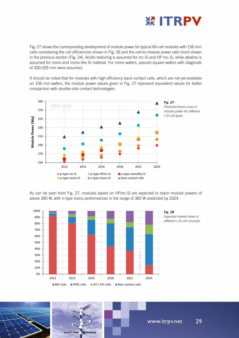
Fig. 27 shows the corresponding development of module power for typical 60-cell modules with 156 mm cells considering the cell efficiencies shown in Fig. 26 and the cell-to-module power ratio trend shown in the previous section (Fig. 24). Acidic texturing is assumed for mc-Si and HP mc-Si, while alkaline is assumed for mono and mono-like Si material. For mono wafers, pseudo-square wafers with diagonals of 200-205 mm were assumed.
It should be noted that for modules with high efficiency back contact cells, which are not yet available on 156 mm wafers, the module power values given in Fig. 27 represent equivalent values for better comparison with double-side contact technologies.
As can be seen from Fig. 27, modules based on HPmc-Si are expected to reach module powers of above 300 W, with n-type mono performances in the range of 360 W predicted by 2024.
Fig. 27Predicted trend curve of module power for different c-Si cell types.
250
270
290
310
330
350
370
390
2013 2014 2016 2018 2021 2024
Mod
ule
Pow
er [W
p]
p-type mc-Si p-type HPmc-Si p-type monolike-Sip-type mono-Si n-type mono-Si back contact cells
ITRPV 2014
Fig. 28Expected market share of different c-Si cell concepts.
0%
10%
20%
30%
40%
50%
60%
70%
80%
90%
100%
2013 2014 2016 2018 2021 2024
BSF cells PERC cells HIT / HJT cells Rear contact cells
ITRP
V 20
14

30
The current edition of the ITRPV predicts a mainstream market for double-sided contact cell concepts – within this market, new approaches like rear-side passivated PERC cells will gain significant market share, as can be seen in Fig. 28. Additionally, heterojunction (HIT/HJT) cells are expected to gain a market share of up to 10% by 2024. The last edition of the ITRPV’s forecast for rear-side contact cells has been reduced by one-third, to slightly over 20% this time around.
Furthermore, it is expected (see Fig. 28) that an increasing number of cells will be light-sensitive on both sides and hence will be bifacial cells. Our research predicts that starting from 2014 the percentage of bifacial cells will steadily increase to a value above 15% by 2024. Since not all bifacial cells will be integrated in bifacial type modules with transparent backsheets or double glass, the proportion of bifacial modules will be smaller than for cells.
In Fig. 29 some important module trends are depicted. Our research shows that a strong increase in market share can be expected for double glass modules in which the backsheet is replaced by a glass pane. We predict that by 2024 roughly 60% of all c-Si modules will be double-glass modules. This trend is enabled by the increased availability of 2 mm hardened front-cover glass panes. Another main driver is the trend towards longer module lifetimes and increased long-term stability, which can be realized by using a double-glass design.
Furthermore, it is expected that by 2021 about 20% of c-Si modules will be frameless (see Fig. 29). However, this requires the development of cost-effective alternative edge protection and mounting technologies.
Fig. 29Market share of different c-Si module types as fraction of worldwide production.
0%
10%
20%
30%
40%
50%
60%
70%
2013 2014 2016 2018 2021 2024
frameless c-Si modules double glass c-Si modules
ITRPV 2014
www.itrpv.net 31
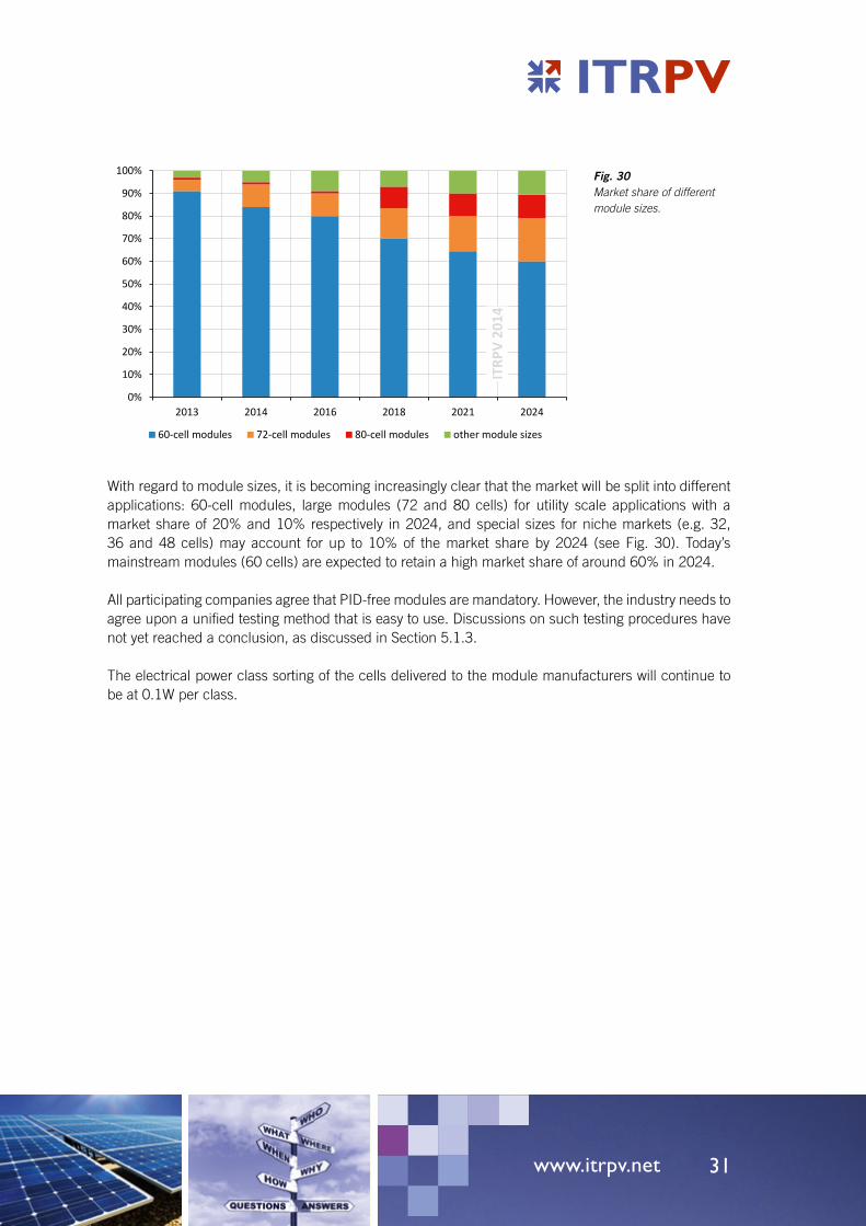
With regard to module sizes, it is becoming increasingly clear that the market will be split into different applications: 60-cell modules, large modules (72 and 80 cells) for utility scale applications with a market share of 20% and 10% respectively in 2024, and special sizes for niche markets (e.g. 32, 36 and 48 cells) may account for up to 10% of the market share by 2024 (see Fig. 30). Today’s mainstream modules (60 cells) are expected to retain a high market share of around 60% in 2024.
All participating companies agree that PID-free modules are mandatory. However, the industry needs to agree upon a unified testing method that is easy to use. Discussions on such testing procedures have not yet reached a conclusion, as discussed in Section 5.1.3.
The electrical power class sorting of the cells delivered to the module manufacturers will continue to be at 0.1W per class.
Fig. 30Market share of different module sizes.
0%
10%
20%
30%
40%
50%
60%
70%
80%
90%
100%
2013 2014 2016 2018 2021 2024
60-cell modules 72-cell modules 80-cell modules other module sizes
ITRP
V 20
14

32
6. PV SystemsDue to the significant reduction of PV module prices over the last few years, balance of system (BOS) costs have become a crucial factor in overall system costs and hence the levelized cost of electricity (LCOE). In Figures 31 and 32 we show the relative development of BOS costs for large systems greater than 100 kWp in Europe, the USA and Asia. It should be noted that no “soft costs”, such as costs for permits or financing, are included as these costs can vary greatly from country to country. Excluding such soft costs, the distribution of BOS costs as well as their development over time is expected to be very similar for Europe and the USA.
As can be seen from Fig. 32, the overall trend of BOS cost reductions of about 30% in 10 years is expected to apply to Asia as well as to Europe and the USA. However, the distribution of inverter, wiring, mounting and ground cost components is noticeably different; indeed, the share of wiring and ground costs in Asia are higher by a factor of two compared to the other two continents.
Fig. 31Relative BOS cost development for systems > 100kW in Europe and US (2013 = 100%).
38% 33% 30% 27% 23% 20%
8%8%
8%8%
8%8%
46%44%
42%40%
38%34%
8%8%
8%8%
8%
8%
100%94%
89%84%
77%
70%
0%
10%
20%
30%
40%
50%
60%
70%
80%
90%
100%
2013 2014 2016 2018 2021 2024
Inverter Wiring Mounting Ground
ITRPV 2014
Fig. 32BOS costs for systems > 100kW in Asia.
32% 27% 24% 22% 20% 17%
15%15% 15% 15%
12% 12%
32%32%
29% 29%27%
24%
22%20%
17% 17%
17%17%
100%
93%
85% 83%
76%71%
0%
10%
20%
30%
40%
50%
60%
70%
80%
90%
100%
2013 2014 2016 2018 2021 2024
Inverter Wiring Mounting Ground
ITRPV 2014

www.itrpv.net 33
As a key component of energy production, the levelized costs of electricity LCOE are of paramount importance when comparing different renewable and non-renewable technologies for electricity generation. In order to demonstrate the potential of PV power generation we calculated the LCOE in USD for large PV Systems under different insolation conditions (see Fig. 33). As the actual system price is highly dependent on the location of the system, we assumed 1,400 USD/kWp in 2013 for our calculation, which is typical for large scale systems in Southern Europe. Taking into account the trends of BOS and module costs depicted in Fig. 31 and Table 3 (next section) respectively, the system costs will reduce to values below 830 USD by 2024.
As can be seen from Fig. 33, LCOE values of between 0.05 and 0.10 USD, depending on the insolation level, are already feasible today. Considering the system price trend expected by the ITRPV, PV electricity costs in the range of 0.03 to 0.07 USD/kWh are predicted by 2024. It should be noted that the LCOE, besides depending on the system price and the insolation level, is strongly influenced by financing conditions and the usable life of the system. For our calculations we have assumed a usable system life of 25 years. However, it is expected that with the progress in module technology as outlined in the ITRPV, the life of a system can reach 30 years and more, which would allow LCOE levels to be reduced even further. This clearly makes PV-power generation a cost-competive clean energy source which will play a major role in worldwide energy supply.
Fig. 33Calculated LCOE values for different insolation conditions. Financial conditions: 80% debt, 5%/a interest rate, 20 years loan tenor, 2%/a inflation rate, 25 years usable system life.
0.1110.102
0.0940.084
0.0740.065
0.0740.068
0.0620.056
0.0490.044
0.056 0.051 0.0470.042
0.037 0.033
14001286
1181
1061
930824
0
200
400
600
800
1000
1200
1400
1600
0.00
0.02
0.04
0.06
0.08
0.10
0.12
0.14
0.16
2013 2014 2016 2018 2021 2024
Assu
med
syst
em p
rice
[USD
/kW
p]
LCO
E [U
SD/k
Wh]
1000 kWh/kWp 1500 kWh/kWp 2000 kWh/kWp assumed system price
ITRPV 2014
34
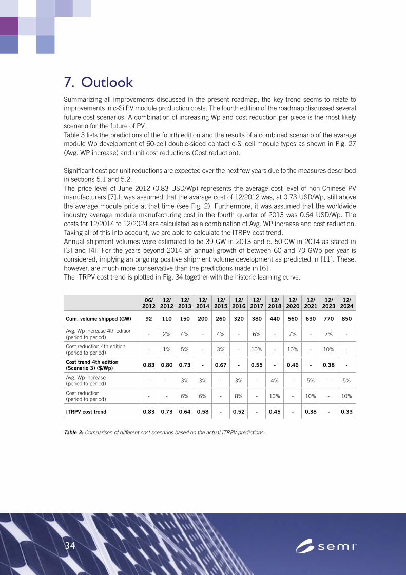
7. OutlookSummarizing all improvements discussed in the present roadmap, the key trend seems to relate to improvements in c-Si PV module production costs. The fourth edition of the roadmap discussed several future cost scenarios. A combination of increasing Wp and cost reduction per piece is the most likely scenario for the future of PV.Table 3 lists the predictions of the fourth edition and the results of a combined scenario of the avarage module Wp development of 60-cell double-sided contact c-Si cell module types as shown in Fig. 27 (Avg. WP increase) and unit cost reductions (Cost reduction).
Significant cost per unit reductions are expected over the next few years due to the measures described in sections 5.1 and 5.2.The price level of June 2012 (0.83 USD/Wp) represents the average cost level of non-Chinese PV manufacturers [7].It was assumed that the avarage cost of 12/2012 was, at 0.73 USD/Wp, still above the average module price at that time (see Fig. 2). Furthermore, it was assumed that the worldwide industry average module manufacturing cost in the fourth quarter of 2013 was 0.64 USD/Wp. The costs for 12/2014 to 12/2024 are calculated as a combination of Avg. WP increase and cost reduction. Taking all of this into account, we are able to calculate the ITRPV cost trend.Annual shipment volumes were estimated to be 39 GW in 2013 and c. 50 GW in 2014 as stated in [3] and [4]. For the years beyond 2014 an annual growth of between 60 and 70 GWp per year is considered, implying an ongoing positive shipment volume development as predicted in [11]. These, however, are much more conservative than the predictions made in [6].The ITRPV cost trend is plotted in Fig. 34 together with the historic learning curve.
06/ 2012
12/ 2012
12/ 2013
12/ 2014
12/ 2015
12/ 2016
12/ 2017
12/ 2018
12/ 2020
12/ 2021
12/ 2023
12/ 2024
Cum. volume shipped (GW) 92 110 150 200 260 320 380 440 560 630 770 850
Avg. Wp increase 4th edition (period to period) - 2% 4% - 4% - 6% - 7% - 7% -
Cost reduction 4th edition (period to period) - 1% 5% - 3% - 10% - 10% - 10% -
Cost trend 4th edition (Scenario 3) ($/Wp) 0.83 0.80 0.73 - 0.67 - 0.55 - 0.46 - 0.38 -
Avg. Wp increase (period to period) - - 3% 3% - 3% - 4% - 5% - 5%
Cost reduction (period to period) - - 6% 6% - 8% - 10% - 10% - 10%
ITRPV cost trend 0.83 0.73 0.64 0.58 - 0.52 - 0.45 - 0.38 - 0.33
Table 3: Comparison of different cost scenarios based on the actual ITRPV predictions.

www.itrpv.net 35
Fig. 34 Learning curve of module price as function of the cumulative PV module shipments with historic data and the ITRPV cost trend shown in Table 3.
The future cost reductions of c-Si modules will cause a shift in the c-Si based PV system cost structure [12] and will therefore enable a sustainable cost reduction for those systems.
Table 3 shows that the industry could reduce costs faster than assumed in the fourth edition of the ITRPV in 2013. The reduction of costs per Wp will be supported by an increase in the Wp/module in parallel with unit cost reductions. The resulting learning rate of 23.5% as shown in Fig. 34 is slightly ahead of the historic learning rate. An increase of module shipments would result in a slight reduction of the learning rate. The ITRPV cost trend assumption shows that the PV industry has begun the process of “learning” once again after the turbulences of recent years. The PV industry can therefore provide power generation products that are competitive with conventional and other renewable sources of energy.
This roadmap was based on data collected from leading international PV manufacturers along the c-Si value chain, PV equipment suppliers, production material providers, and PV institutes in 2013. An annual update of this information is planned. Topics such as wafer thickness require cooperation between tool suppliers, cell manufacturers and other entities along the value chain. A download of the current issue of this document and information about how to get involved in the roadmap activity are available on the website at www.itrpv.net.
ITRPV 2014
10 -1 10 0 10 1 10 2 10 3 10 4 10 5 10 6 10 70,1
1
10
100
10 -1 10 0 10 1 10 2 10 3 10 4 10 5 10 6 10 7
0,1
1
10
100
aver
age
mod
ule
sale
s pric
e (U
SD 2
011/
Wp)
cumulative PV module shipments (MWp)
ITRPV cost trend LR 23,5%
historic data LR 21.5%

36
8. References[0] Stefan de Haan, IHS Solar, personal information
[1] F. Kersten, R. Doll, A. Kux, D. M. Huljic, M. A. Görig, C. Berger, J. W. Müller. P. Wawer, “PV learning curves: past and future drivers of of cost reduction”, Proceedings of 26th European Photovoltaic Solar Energy Conference,pp. 4697-4702, 2011.
[2] A. Ristow, “Compilation of pricing and cumulated c-Si-PV installations” based on data published in : i) Maycock, „The World Photovoltaic Market 1975-2001“, PV Energy Systems, 2001, ii) “PVNews”, Prometheus Institute & Greentech Media, 2005 till 2010, iii) Mehta, „PV News annual data collection results: 2010 cell, module production explodes past 20 GW“, GTM Research, May 2011 and iv) EPIA-market-report-2011, www.epia.org, TOTAL Energies Nouvelles, Paris la Defense, France, 2013.
[3] V. Shah, J. Booream-Phelps, Susie Min, Deutsche Bank Markets ResearchIndustry update Solar Industry, “2014 Outlook: Let the Second Gold Rush Begin”, Deutsche Bank AG, Januar 2014.
[4] Stefan de Hann, in IHS iSuppli Whitepaper, “Predictions for the Solar Industry in 2014 – Top 10 Trends for the Year Ahead”, IHS iSuppli, www.isupplis.com/Photovoltaics/News, December 2013.
[5] EPIA press release, “World’s solar photovoltaic capacity passes 100-gigawatt landmark after strong year”, www.epia.org/news/press-releases, Brussels, February 2013.
[6] A. Gerlach, “Data compilation” from: i) Bloomberg New Energy Finance https://surveys. bnef.com/, ii) Energy Trend http://pv.energytrend.com, iii) Photon Consulting “The Wall” www.photonconsulting.com/thewall/, and iv) PV Insights www.Pvinsights.com, Hanwha Q.Cells GmbH, Bitterfel-Wolfen, Germany, 2014.
[7] S. Mehta, “GLOBAL PV MODULE MANUFACTURERS 2013: Competitive Positioning, Consolidation and the China Factor”, GTM Research, October 2012.
[8] Nathaniel Bullard, “CHINA‘S 12GW SOLAR MARKET OUTSTRIPPED ALL EXPECTATIONS IN 2013”, Bloomberg New Energy Finance (BNEF), January 2014.
[9] H. Wicht, “Silicon Pricing Trends Price developments of various grades of Silicon”, 10th Photon’s Solar Silicon Conference, Berlin, March 2012.
[10] Kane, IEEE PVSEC, 18, 1985.
[11] EPIA, “Global market outlook for photovoltaics 2013-2017”, www.epia.org, Brussels, March 2013.
[12] A. Goodrich et. al., “Residential, Commercial, and Utility-Scale Photovoltaic (PV) System Prices in the United States: Current Drivers and Cost-Reduction Opportunities”, technical report, NREL/TP-6A20-53347, February 2012.

www.itrpv.net
About SEMI – Solar/PVSEMI member companies provide equipment, and materials to enable photovoltaics manufacturing. Our mission is to advance industry growth, support continuous efficiency improvements and promote sustainable business practices through international standards development, events, public policy advocacy, EHS support, market intelligence, and other services.
www.semi.org/PVwww.itrpv.net
SEMI OfficesSEMI EuropeMr. Stephan RaithelHelmholtzstrasse 2-9Haus D / 3.OG10587 BerlinGermany
+49 30 3030 8077 [email protected]
SEMI ChinaMr. Toby LiuRoom 201, Bldg. 2295 Zuchongzi RoadZhangijang Hi-tech ParkPudong, 201203 ShanghaiP.R. China
+86 21 6027 [email protected]
SEMI TaiwanMr. Paxon Lee11F-2, Taiyuan 1st St.,Zhubei City,Hsinchu County,30265, Taiwan
+886 3 573 3399 ext [email protected]
SEMI USMrs. Bettina Weiss3081 Zanker RoadCA 95134 San JoseUSA
+1 408 943 [email protected]