intensity control of dielectric barrier discharge...
TRANSCRIPT


INTENSITY CONTROL OF DIELECTRIC BARRIER DISCHARGE FILAMENTS
by
MATTHEW CRAWFORD PALIWODA
A THESIS
Presented to the Faculty of the Graduate School of the
MISSOURI UNIVERSITY OF SCIENCE AND TECHNOLOGY
In Partial Fulfillment of the Requirements for the Degree
MASTER OF SCIENCE IN AEROSPACE ENGINEERING
2016
Approved by
Joshua L. Rovey Ph.D., Advisor
Xiaodong Yang, Ph.D
Carlos H. Castano, Ph.D


iii
ABSTRACT
When operated in a filamentary mode, a volume dielectric barrier discharge
(DBD) is known to produce patterned plasma structures. These structures are currently
being explored for reconfigurable metamaterial applications. In this work the presence
and intensity of a single filament, within an array of filaments, was controlled by
adjusting the voltage to that filament’s individual needle electrode. The current, voltage,
and time-averaged normalized light intensity were measured while varying the voltage of
the needle through a self-biasing resistance. For a 7.5 kV, 3.2 kHz DBD in air, the
needle-controlled filament intensity varies from that of the surrounding filaments to zero
measurable light intensity. The total bias on the needle does not exceed 7 % of the
driving voltage. Analysis of an electrostatic field model showed that the varying intensity
filament does not produce light when the curve of the electric field along the filament
centerline is below the curve of the electric field along the centerline of an adjacent
unbiased filament. Surface charge interaction, on the dielectric barrier furthest from the
needle electrode, is the mechanism that extinguishes the filament while the applied
electric field is above the dielectric strength of air. The light intensity was calculated as
the total charge transferred across the filament. The total charge was estimated from the
simulation model and varies with the measured light intensity.

iv
ACKNOWLEDGMENTS
I am extremely grateful to my advisor, Dr. Joshua Rovey, for the opportunity,
support and guidance over the past two years. The laboratory independence and freedom
to pursue different avenues of thought made the research experience an absolute pleasure.
I would like to thank both Dr. Rovey and the Aerospace and Mechanical
Department at Missouri S&T for the graduate research assistant positions and the
graduate teaching position that provided financial support for this degree.
I would like to thank my committee members Dr. Carlos Castano and Dr.
Xiaodong Yang for their assistance and insight.
I would like to thank my fellow students and friends for their technical and moral
support: Dr. Warner Meeks for his mentorship in the laboratory, Mitch Wainwright for
his computer simulation work on this project, and Joshua Heck for assistance finishing
the thesis.
Finally, I would like to thank my family and friends for their advice, support, and
proof reading. To my parents, thank you for everything.

v
TABLE OF CONTENTS
Page
ABSTRACT ....................................................................................................................... iii
ACKNOWLEDGMENTS ................................................................................................. iv
LIST OF ILLUSTRATIONS ............................................................................................ vii
NOMENCLATURE ........................................................................................................ viii
SECTION
1. INTRODUCTION ...................................................................................................... 1
1.1. METAMATERIALS .......................................................................................... 1
1.2. PLASMA AS METAMATERIAL ..................................................................... 2
1.3. DBD AS A RECONFIGURABLE METAMATERIAL .................................... 4
1.4. FOCUS OF CURRENT WORK ......................................................................... 5
1.5. PARAMETERS OF DBD PLASMA ................................................................. 6
1.6. STREAMER DISCHARGE THEORY .............................................................. 7
2. EXPERIMENTAL SETUP ........................................................................................ 9
2.1. VOLUME DBD PHYSICAL AND ELECTRICAL SETUP. ............................ 9
2.2. NEEDLE ELECTRODE SETUP ..................................................................... 11
3. EXPERIMENTAL RESULTS ................................................................................. 12
3.1. FILAMENT PHOTOGRAPHS ........................................................................ 12
3.2. NEEDLE CURRENT AND VOLTAGE .......................................................... 14
3.3. INCREASED FILAMENT INTENSITY ......................................................... 15
3.4. EFFECT OF RESIDUAL CHARGE ................................................................ 17
4. ELECTRIC FIELD MODELING ............................................................................ 19
5. RESULTS ................................................................................................................. 21
5.1. LONGITUDINAL ELECTRIC FIELD ............................................................ 21
5.2. POTENTIAL..................................................................................................... 22
5.3. TRANSVERSE ELECTRIC FIELD ................................................................ 23
5.4. FREE SURFACE CHARGE LIMITATION. ................................................... 24
6. DISCUSSION .......................................................................................................... 27
6.1. FILAMENT EXTINGUISHING MECHANISM............................................. 27

vi
6.2. LIGHT INTENSITY RELATIONSHIP ........................................................... 28
7. CONCLUSION ........................................................................................................ 32
BIBLIOGRAPHY ............................................................................................................. 34
VITA ................................................................................................................................ 40

vii
LIST OF ILLUSTRATIONS
Page
Figure 2.1. Photograph of DBD setup.. ........................................................................... 10
Figure 2.2. Diagram of experimental set up. ................................................................... 11
Figure 3.1. Photographs of the filament at the needle: on and off.. ................................. 13
Figure 3.2. Light intensity as a function of resistance at 6.5kV, 7.5kV, and 9.0kV. ....... 14
Figure 3.3. Voltage and current as a function of resistance at 6.5kV and 7.5kV. ........... 15
Figure 3.4. Photographs of the decreasing filaments surrounding the needle position. ... 16
Figure 3.5. Light intensity as a function of resistance for a self-biased mesh. ................. 17
Figure 3.6. Light intensity of the acetone and non-acetone treatment as a function of
resistance at 9.0kV.. ........................................................................................ 18
Figure 3.7. DBD voltage for the acetone and non-acetone treatment as a function of
resistance at 9.0kV. ......................................................................................... 18
Figure 4.1. Isometric view of the 3D CST model. ............................................................ 20
Figure 5.1. Contour of longitudinal electric field. ............................................................ 22
Figure 5.2. Difference between needle and mesh centerline electric field. ...................... 22
Figure 5.3. Difference between needle and mesh centerline potential.. ........................... 23
Figure 5.4. Transverse electric field as a function of x-position ...................................... 24
Figure 5.5. Contour map of the displacement field on the cathode dielectric surface, at
0.2MΩ. ............................................................................................................ 26
Figure 5.6. Ratio of needle to mesh charge, on the cathode dielectric. ............................ 26
Figure 6.1. Potential difference between the needle and mesh on the anode dielectric
surface. ............................................................................................................ 28
Figure 6.2. Calculated and measured light intensity as a function of resistance. ............. 31

viii
NOMENCLATURE
Symbol Description
A Surface Area
B Magnetic Field
Bavg Average Magnetic Field
D Displacement Field
Davg Average Displacement Field
E Electric Field
Eavg Average Electric Field
Eo Baseline Electric Field
Er Electric Field of Electron Avalanche
H Magnetic Strength
Havg Average Magnetic Strength
G|| Translation Vector
Je Electron Current Density
J1 Bessel Function
L Path Length
R Filament Radius
S Integral Surface
V Voltage
a Lattice Constant
e Elementary Charge
me Electron Mass
n Surface Normal Unit Vector
ne Electron Number Density
ng Neutral Gas Number Density
nineg Negative-Ion number Density
nipos Positive-Ion Number Density
p Pressure
q Surface Charge

ix
r Surface Charge Area Radius
t Time
to Streamer Initiation Time
ue Electron Drift Velocity
x Position Parallel to Dielectric Surface
z Position Across the Air Gap
First Townsend Coefficient
Effective Permittivity
Permittivity of Free Space
Permittivity in Fourier space
κ Inverse Fourier Coefficient
Effective Permeability
Volume Charge Density
Electron-Neutral Collision Frequency
Surface Charge Density
Electron-Neutral Collisional Cross-Section
Electric Potential
Light Intensity Flux Rate
Time-Space Integrated Light Intensity
Incident Electromagnetic Wave Frequency
Plasma Electron Frequency

1. INTRODUCTION
Filamentary plasma has been previously studied for application in the growing
field of microwave metamaterials due to its electrically variable structure, variable
negative permittivity, and sub-microwave scale. 1-9
Metamaterials are artificial periodic
composite structures that create permittivities and permiabilities not commonly found in
nature, including negative values. Manipulation of these two material properties leads to
unique propagation of electromagnetic waves through the material, such as negative
refraction. Metamaterials have application in communication, radar, signal processing,
energy transfer, and non-destructive sensing.
1.1. METAMATERIALS
A metamaterial modifies electromagnetic wave propagation by resonating with
the wave fields on a subwavelength scale, inducing opposing electromagnetic fields and
shifting the average displacement field/magnetic field away from the average electric
field/magnetic field strength, as expressed in Equation 1. Pendry et al. initially discussed
filling space with thin wire resonators to allow wave propagation bellow the plasma cut-
off frequency of the wire10
as well as the relocation of electromagnetic energy to modify
the permeability and permittivity of split ring resonators.11
avgo
avg
effE
D
(1a)
avgo
avg
effH
B
(1b)
For a metal wire hexagonal lattice structure, the relation between the geometric
arrangement of the wires – defined by the wire radius and the separation between
wires or lattice constant , – and the material properties of the metal wires – defined by
the electron frequency and the permittivity of the surrounding gas , –
determines the effective perimittivity ( of the composite material, as expressed in

2
Equation 2 and Equation 3.12
The permittivity is expressed in its inverse Fourier
coefficients in Equation 4, whereby is the position vector of the lattice structure,
is the frequency of the incident electromagnetic wave, and is the translation
vector, a function of the reciprocal lattice. Numerical methods are used to define more
complex structures that do not have an analytical solution.
||
||||)()|( ||||
G
xjGeGx (2)
0,33
21
1
33
2)( ||2
2
2
2
22
2
||
G
a
R
a
R
jv
jvG
gpec
c
(3)
0,),(
),(2
33
21)( ||
||
||1
2
2
22
2
||
G
RG
RGJ
a
R
jv
jvG
gpec
c
(4)
1.2. PLASMA AS METAMATERIAL
Plasma’s non-linear permittivity makes it a prime candidate for metamaterial
application. The complex plasma permittivity is defined by Equation 5,13
dependent upon
the incident wave frequency ( ), the electron plasma frequency ( , and the collisional
frequency ( . By adjusting the plasma frequency, the permittivity can be tuned between
unity and negative values of permittivity for a given incident wave frequency.
2222
2
1c
cpe
c
pe
effv
v
jv
(5)
Structures providing negative permeabilities, such as ring resonators and helix
structures,14
immersed in plasma have been investigated for creating a negative index of
refraction metamaterial. In these structures, plasma is the component that provides the
negative permittivity. Another benefit of plasma is that it provides electrical variability,

3
since the electron frequency is related to the plasma density ( ) by Equation 613
and
varies with the applied voltage and frequency.9, 15
By tuning the plasma’s electron
density, a desired permittivity can be obtained during operation. This creates a variable
index of refraction, or range of frequencies, over which the metamaterial can function.
eo
epe
m
en
2
(6)
Another aspect of the plasma is its physical malleability, forming plasma as a
periodic structure instead of as a homogeneous material. The permittivity can be further
altered by changing the lattice constant of the structure. Then the permittivity is then
dependent upon the plasma structure in addition to the electron density and collisional
frequency. Thus, by varying the structure, the bandwidth for a given permittivity is
extended.
A large variety of solid variable metamaterials in the microwave frequency have
been investigated.16
However, variability of these structures is limited by their electrical
and structural components. The demonstrated bandwidth is on the order of ~5GHz.
Plasma metamaterial variability is limited only by the electron density and the bounds
that define its physical structure, providing a potentially larger bandwidth.
In addition to being tunable, the plasma can sustain high energy waves without
failure due to its inherent high energy state. High power microwaves (HPM), defined by
Benford and Swegle17
as frequencies between 1 and 300GHz and peak power levels
above 100 MW, are a potential niche area for plasma metamaterial application. Solid
metamaterials have been investigated for HPM; however, gas breakdown,18
material
combustion,19
and losses from failed components20
due to large electric fields between
components of a centimeter scale have proven to be an issue. For plasma based
metamaterials, gas breakdown defines the microstructure, which eliminates ionization as
a design limitation. Application of high energy microwaves includes directed energy
weapons, plasma heating, radar, communication systems, and high energy particle
research.17, 21, 22
4
1.3. DBD AS A RECONFIGURABLE METAMATERIAL
Filamentary dielectric barrier discharge (DBD) as a potential metamaterial is of
particular interest due to its inherent microstructure. A DBD plasma filament is formed
by discharging gas between two parallel plates that are covered with dielectric material,
producing filaments ( plasma columns ~0.1 mm in diameter ) across the gas gap.23, 24
The
filaments have surface charges on the dielectric and space charges in the gas gap which
interact with one another.25
These dynamics limit the number of neighboring filaments;
creating a memory effect that promotes filament restrike at the same location during the
reversed polarity of the AC voltage.25, 26
These filaments and their dynamics provide the
structural element and mechanism to define a two dimensional microstructure made of
plasma columns, similar to the thin rod metamaterials.
The filaments’ interaction with an incident electromagnetic wave is defined by
their permittivity. They support electric fields parallel with the plasma columns
(transverse electric waves – TE waves), similar to wire photonic crystals, as well as
plasmons that travel around the column surfaces created by the interface between the
negative and positive permittivities (transverse magnetic waves – TM waves).27
Research using plasma filaments to construct metamaterials and affect the
propagation of electromagnetic waves has focused on plasma photonic crystals (PPC) for
application to microwaves.9 Sakai et al
7 used individual cathode electrodes without a
dielectric surface to demonstrate that bandgaps occur in plasma filament photonic
crystals.6 In addition to the plasma potential for bandgap waveguides, Sakai et al
7
demonstrated a waveguide consisting of a single row of filaments transmitting a signal
around a ninety degree turn. Dong et al2-4
has focused on demonstrating the formation of
plasma structures in self-organized DBDs, and then numerically modeling the resulting
bandgaps. Zhang et al,28-30
conducted numerical models on exotic two dimensional
plasma structures, exploring more diverse band structures than those previously
demonstrated in self-organized DBDs. Methods for solving arbitrary geometries
numerically for band gaps have been developed so that more elaborate geometric
structures may be analyzed.29, 30
For these geometries, direct control of the plasma
position would be necessary to physically recreate their effect.

5
Plasma filaments are similar to the thin metal rods in previously demonstrated
metamaterials since both permittivities are described by the Drude model, Equation 5.
Although metal rods serve best to excite changes in the permittivity when resonating with
TE waves, Park and Wu31
demonstrated a negative permeability excited by TM waves
using square clusters of metal rods. The clusters enhanced the magnetic dipoles created
by the electric field traveling around the cluster, perpendicular to the filament axis.
Further, they numerically calculated a negative index of refraction with the composite of
negative permeability wire clusters and negative permittivity metal components.32
Plasma’s capability for negative permittivity and the potential to create a negative
permeability through filament clusters suggests a similar plasma composite could
produce negative index of refraction.
1.4. FOCUS OF CURRENT WORK
Control of the filament structural position has been demonstrated using both fixed
electrode arrays6-8
and self-organized DBDs.1-5
The self-organized filament DBDs form
organized structures over the entire surface of a DBD due to limiting interactions
between filaments. However these organized structures link structure, filament size, and
electron densities to the two independent variables of driving frequency and applied
voltage. They are also limited to a maximum lattice dimension on the order of the
filament’s surface charge and there is no direct method for implementing predesigned and
simulated structures.
Fixed individual electrode filaments allow for direct position control of the
filaments but limit the variety of structural arrangements in the PPC to the grid assembly
of the individual electrodes. Those demonstrating individual control over each electrode
require a kilovolt switching or separate driving mechanism. Self-organizing DBD
structures using arrays of individual electrodes have been demonstrated3, 8
and show that
filament discharges can occur in between electrode surface positions, extending the
bandwidth of the system; however, for these demonstrations, each electrode was driven
by the same voltage.

6
The eventual goal of the presented work is to form electrode arrays behind a
dielectric individually controlling the filaments over the entire surface of the dielectric.
The application could then be extended to discharging filaments between the electrode
surface positions and manipulating the filaments with the surrounding electrode
potentials. Since the total average voltage can be increased while maintaining relative
voltage differences between individual electrodes, the electron density and position
become uncoupled. By using voltage to control the filament position, the structural tuning
remains electrical. The position and electron density of each filament is then
independently controlled with electrical signals over the entire surface of the dielectric.
With this approach, a larger range of effective permittivities may be directly implemented
during DBD operation.
1.5. PARAMETERS OF DBD PLASMA
The applied conditions for a DBD plasma, such as gas pressure, gas species,
voltage, and frequency determine the two defining parameters of a plasma microstructure
element: the permittivity and the filament’s radius. DBD filaments have electron densities
of 1013
-1015
(cm-3
).33
At atmospheric pressure in air the neutral gas density is 2.5 x 10¹⁹
kg/cm3. This makes the degree of ionization < 10
-3 %, defining the gas as weakly ionized,
where the main form of collision is with neutrals. The collision frequency is then
dependent upon the pressure and molecular make up of the gas. For the presented results,
atmospheric air was used, defining a collision frequency of 260 GHz and estimated using
Equation 7.34
The collision frequency ( ) is equal to the product of the neutral gas
number density ( ), the electron-neutral collisional cross-section ( ),35
and the drift
velocity ( ).36
The parameters are dependent upon the electron temperature ( ), which
can range from 1-10eV33
but is 3-4eV37
for the presented experimental condition. The
electron temperature does not change with pressure, and is weakly proportional to the
driving voltage.15
eengc unv (7)

7
The cut-off electron frequency, calculated using Equation 6, under which an
incident wave will experience a negative permittivity, is 30GHz to 300GHz. These
frequencies produce wavelengths in the microwave range of 10mm to 1mm. With a
defined pressure and gas species, the electron density is determined by the applied DBD
voltage and frequency.15
The filament diameter is a lower dimensional bound to the
applicable incident wavelength. For a fixed pressure, the radius of the filament depends
upon the driving voltage38
and frequency.39
1.6. STREAMER DISCHARGE THEORY
The type of discharge that forms DBD plasma columns is a streamer discharge.
The theory was initially developed by Meeks, Loeb, and Raether40, 41
to describe the
disagreement between Townsend discharge and the observed discharge which precedes
an arc. The streamer initiates with a Townsend discharge where an electron avalanche
travels across the gas gap towards the anode. The difference between ion and electron
drift velocities forms a concentration of electrons at the avalanche head and a trail of
relatively stationary ions, creating a strong local electric field distortion at the head that
opposes the applied electric field. The radius of the avalanche head grows due to
diffusion and defines the field at the head. When the avalanche grows large enough for
the distorted field to equal the applied field, electrons near the head experience a total
force towards the head causing an intense multiplication of ionizations. Increased photons
produced by ionization at the avalanche head increase secondary photoionization. The
secondary electrons ahead and behind the streamer create a conductive path for the
streamer to travel. The streamer then grows at the faster rate of the traveling
photoionization process across the gap rather than the electron drift velocity.
Two types of streamers can form: either a positive or a negative streamer. They
are directed in the positive or negative electric field direction. Photoionization leads the
positive streamer towards the cathode along the distorted tail of the electron avalanche,
extending the streamer with successive ionizations and directing the electrons through the
conductive path of the streamer. Photoionization for a negative streamer leads the
streamer towards the anode by creating sequential avalanches ahead of the initial

8
avalanche tip that provide a conductive path of ions for streamers electrons to travel
along. Positive streamers are more often observed than the negative streamers and
produce lower electron densities.42
After the streamer reaches both dielectric surfaces, the streamer acts as a highly
conductive path for charge to transfer across. Surface charge builds up on the dielectric
and distributes radially from the streamer. Built-up charge eventually shields the streamer
from the applied electric field until the field driving the ionization process drops below
the dielectric strength of air. At this point, the streamer is extinguished. Residual space
and surface charge increases the electric field at the location of the streamer during the
reversed polarity of the applied electric field so that another streamer discharges at the
same location. The surface charge and space charge create a memory effect that causes
the time-averaged light from multiple filaments to maintain its position.

9
2. EXPERIMENTAL SETUP
2.1. VOLUME DBD PHYSICAL AND ELECTRICAL SETUP
The DBD investigated in this work consists of two parallel copper mesh
electrodes, both covered with microscope slide glass. The driving signal mesh electrode
allows for end-on photos of the filament position across the surface of the dielectric. The
mesh and dielectric barrier of the driving electrode are of dimensions that create a
uniform charge distribution over the discharging surface: 0.15 mm opening (#100 mesh
size), 0.056 mm wire diameter, and 1.0 mm thick dielectric.43, 44
The grounded mesh
electrode has an opening of 0.85mm (#20 mesh size), a 0.40 mm diameter wire, and a
dielectric barrier thickness of 0.12 mm. The larger mesh size and thinner dielectric barrier
are sufficient to create an electric field on the surface of the grounded dielectric barrier
that causes filaments to preferentially discharge at the mesh nodes. The wire weave of the
mesh used for the grounded electrode has an offset between the vertical and horizontal
directions that keeps the vertical weave 0.12 mm away from the glass. The peak to peak
sinusoidal amplitude of the horizontal wire weave is 0.92 mm and the vertical wire weave
is 0.68 mm.
The DBD is mounted on an ABS plastic stand with acme screws on the side to
permit fine tuning of the gap width. The air gap between the two plates is set at 1.0 mm.
The mesh electrodes and dielectric cover a 22 mm by 22 mm area. Adhesive gel on the
edge of the mesh prevents charge from making a direct path to the electrodes and thus
ensures the current travels through the dielectric. A photograph of the DBD is shown in
Figure 2.1. The DBD is operated at 6.5 kV, 7.5 kV, and 9.0 kV at 3.2 kHz.
A Canon EOS Rebel XL records the time-averaged discharge of the filament
position and light intensity at an exposure time of 125 seconds. As shown in the electrical
schematic of Figure 2.2, the driving voltage signal is created by a Rigol DG-1022
Function Generator, the power is supplied by a Crown Macro-Tech 1202 Audio
Amplifier, and a Corona Magnetics 5525-2 Transformer with a turn ratio of 1:357
increases the voltage signal producing a maximum voltage of 25 kV with a frequency
range of 0.9 – 5 kHz. A North Star PVM-5 High Voltage Probe, with a 1:1000 ratio,
monitors the voltage supplied to the DBD. A 1:1 Pearson Current Probe, Model 114,

10
monitors the current through the system. A 1:10 Tektronix P2221 passive voltage probe
reads the voltage across a 200kohm resistor in series with the larger resistor controlling
the voltage at the positioned needle. Both the Pearson and the North Star Probes are
recorded by an Agilent Infinium 500MHz 1GSa/s Model #54815A Oscilloscope.
Figure 2.1. Photograph of DBD setup. The DBD consists of two parallel glass plates
backed with (a) powered electrode and (b) grounded electrode. The air gap is controlled
by (c) acme screws. Voltage across the (d) biasing resistors is measured using a voltage
divider with (e) a 200kΩ reference resistor and (f) 10:1 voltage probe. Both grounded
electrode and the voltage divider are referenced to (g) ground. Current supplied from the
(h) transformer is limited by (i) a 5.9kΩ resistor to protect the transformer. The lead from
the (j) high voltage probe measures voltage across the DBD.

11
Figure 2.2. Diagram of experimental set up.
2.2. NEEDLE ELECTRODE SETUP
An independently electrically controlled needle is used to control the intensity of
a plasma filament within the DBD. The needle and its electrical setup are shown in
Figure 2.1 and Figure 2.2. The needle is constructed from a magnetic wire with flattened
tip mounted flush to the back surface of the grounded dielectric barrier. The wire
(diameter 0.57 mm) with an added Kapton insulation layer (0.14 mm thickness, ε = 3.5)
is centered between the mesh so that the only electrical connections between the two are
through the dielectric or their respective lead wires. Resistors connect the needle to
ground causing the needle to have a non-zero floating potential or self-biasing potential.
By adjusting the resistance, the self-biasing potential of the needle can be adjusted.

12
3. EXPERIMENTAL RESULTS
The following section presents the results from needle-controlled filament tests in
the DBD. In some cases the DBD has 1mm gas gap, the voltage is set at 6.5 kV or 7.5
kV. When the driving voltage is at 9.0 kV, the air gap is at 1.5mm. Results are shown
below for different DBD voltages, needle electrode self-biasing resistances, surface
cleansings, and mesh self-biasing resistances.
3.1. FILAMENT PHOTOGRAPHS
Photographs of the DBD filaments for different self-biasing needle resistances are
shown in Figure 3.1. This data is for the 6.5 kV DBD driving voltage. The regular pattern
of dots is made up of individual DBD plasma filaments. The filaments form at alternating
nodes over the grounded wire mesh electrode since the meshes’ vertical wires are slightly
below the mesh surface plane and cannot make a connection. For resistances below 4.7
MΩ, a filament clearly forms in between the wire mesh nodes at the needle location. As
the needle’s self-biasing resistance increases the filament light intensity decreases. It is
clear from these photographs that the independent needle can control both the presence
and intensity of the new filament. Resistance below 200 kΩ was investigated with a 1 kΩ
resistor, however, prominent current spikes reduced the reliability of the measurement.
Resistances above 30 MΩ were not investigated because the data showed further
increases had no effect on the discharge of the filament.
To get a better measure of the intensity change at the needle-controlled filament, a
photographic analysis was conducted. The numerical value of the photograph pixels at
the needle-controlled filament location were compared with the pixel values for mesh
filament and for a region with no filament (i.e., the mid-point between two mesh
filaments). An 8x8 pixel square section of the photograph, fitting the size of the filament,
was selected using Photoshop software and the average luminosity value of the area was
used as the intensity value. A 15x15 size square section was used to select the average
value of a region without any discharge and was subtracted from the intensity values. In
this way the intensity of the needle-controlled filament was compared with a mesh
13
filament and also a region where there was no discharge. Figure 3.2 (b) shows the results
as the ratio of the needle filament to the mesh filament and Figure 3.2 (a) shows the ratio
of the needle filament to the background intensity for 6.5kV, 7.5kV, and 9.0kV. The error
bars were created by taking the standard deviation of ten mesh node filaments between
photos, averaging that deviation, and creating its ratio with the respective plot intensity.
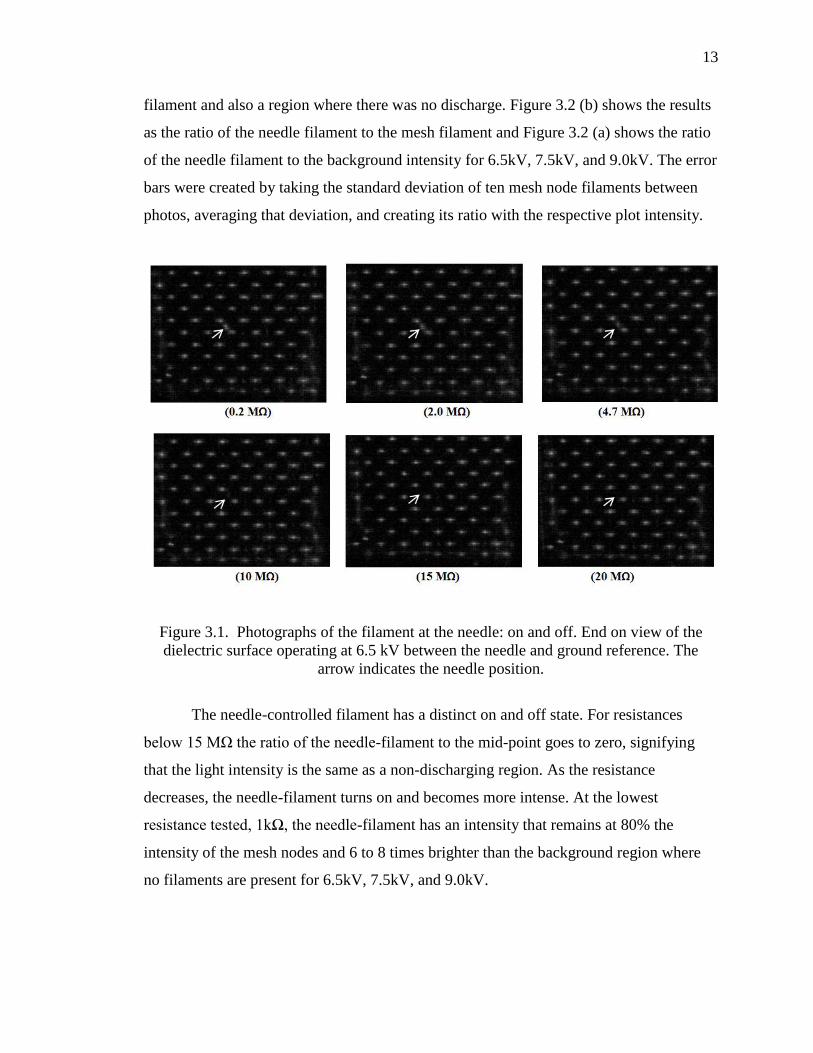
Figure 3.1. Photographs of the filament at the needle: on and off. End on view of the
dielectric surface operating at 6.5 kV between the needle and ground reference. The
arrow indicates the needle position.
The needle-controlled filament has a distinct on and off state. For resistances
below 15 MΩ the ratio of the needle-filament to the mid-point goes to zero, signifying
that the light intensity is the same as a non-discharging region. As the resistance
decreases, the needle-filament turns on and becomes more intense. At the lowest
resistance tested, 1kΩ, the needle-filament has an intensity that remains at 80% the
intensity of the mesh nodes and 6 to 8 times brighter than the background region where
no filaments are present for 6.5kV, 7.5kV, and 9.0kV.

14
Figure 3.2. Light intensity as a function of resistance at 6.5kV, 7.5kV, and 9.0kV. Light
intensity at the needle position (a) as a ratio to the light intensity of a mesh gap midpoint
(no filament) and (b) as a ratio to a mesh node filament.
At 1 kOhm, the needle filament intensity is still less than the surrounding node
filaments. Since the needle filament is surrounded by two other node filaments, it
competes for surface charge with these nodes. If the needle filament was not surrounded
by two other filaments we expect its ratio would rise to near 1 at 1 kΩ resistance. As the
resistance increases, the filament eventually stops discharging. At this point the ratio of
the needle filament to the non-discharging midpoint is zero since the background is
subtracted from the needle value. Assuming there is no discharge in the mesh gap, this
ratio signifies that no discharge occurs at the needle’s position. The measured luminosity
in the regions without filaments is due to ambient light. The camera’s photos also have an
inherent background light value that contributes to the intensity.
3.2. NEEDLE CURRENT AND VOLTAGE
Adjusting the needle self-biasing resistance affects the needle voltage and current.
These results are shown in Figure 3.3. The voltage at the needle does not rise linearly as
it begins to curve with increased resistance. Although the voltage appears as though it
may approach a limit, the point of interest where the filament at the needle ceases to
discharge is met before any definitive evidence of a limit. The voltage for the turn off of
the filament at the needle is 476V and 560V respective to the driving voltages 6.5kV and
( a ) ( b )
15
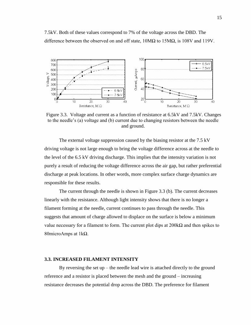
7.5kV. Both of these values correspond to 7% of the voltage across the DBD. The
difference between the observed on and off state, 10MΩ to 15MΩ, is 108V and 119V.
Figure 3.3. Voltage and current as a function of resistance at 6.5kV and 7.5kV. Changes
to the needle’s (a) voltage and (b) current due to changing resistors between the needle
and ground.
The external voltage suppression caused by the biasing resistor at the 7.5 kV
driving voltage is not large enough to bring the voltage difference across at the needle to
the level of the 6.5 kV driving discharge. This implies that the intensity variation is not
purely a result of reducing the voltage difference across the air gap, but rather preferential
discharge at peak locations. In other words, more complex surface charge dynamics are
responsible for these results.
The current through the needle is shown in Figure 3.3 (b). The current decreases
linearly with the resistance. Although light intensity shows that there is no longer a
filament forming at the needle, current continues to pass through the needle. This
suggests that amount of charge allowed to displace on the surface is below a minimum
value necessary for a filament to form. The current plot dips at 200kΩ and then spikes to
80microAmps at 1kΩ.
3.3. INCREASED FILAMENT INTENSITY
By reversing the set up – the needle lead wire is attached directly to the ground
reference and a resistor is placed between the mesh and the ground – increasing
resistance decreases the potential drop across the DBD. The preference for filament

16
discharge is switched to the needle. As the potential on the mesh increases, the larger
potential drop across the air gap between the needle and driving electrode draws more
charge from the surrounding surface. Figure 3.4 shows the resulting filament changes
from reversing the self-biasing process.
Figure 3.4. Photographs of the decreasing filaments surrounding the needle position. End
on view of the dielectric surface operating at 6.5 kV with increasing resistances between
the mesh electrode and ground reference. The surrounding filaments turn off while the
needle filament intensity grows.
The reduction in the available surface charge decreases the intensity of the
surrounding filaments until the mesh node filaments that are one mesh gap unit-distance
away from the needle position have an intensity level less than double the mid-mesh
(ambient) intensity. The two mesh nodes immediately adjacent to the filament also
reduce in intensity. However, two high intensity points occur between the needle and
these mesh nodes, at 1MΩ. Resistances beyond 1MΩ were not investigated since the
current wave forms suggested a transition away from the preferred filament discharge to
that of an arc between the needle and mesh electrodes, which might damage the set up.
Due to the interaction with more than 10 surrounding filaments, the intensity of
the needle filament, shown in Figure 3.5, is significantly different than the self-biased

17
needle intensity results of Figure 3.1. The change observed with the self-biased mesh
occurs over a logarithmic space where orders of magnitude resistance change are required
to increase the intensity of the needle filament. The maximum voltage created by the
1MΩ resistance was measured as 470V and the light intensity was 178% of the
unaffected mesh filaments.
Figure 3.5. Light intensity as a function of resistance for a self-biased mesh. Light
intensity at the needle position as a ratio to mesh filament intensity from unaffected areas
of the DBD.
3.4. EFFECT OF RESIDUAL CHARGE
Charge build up on a DBD affects the charge transfer.23
To analyze the effect of
residual charge between consecutive data points, the charge was removed with acetone,
the 9.0kV conditions were replicated, and compared with the previous data. The acetone
was applied to a Kimwipe wrapped over a razor blade in order to fit into the air gap. Both
dielectric surfaces were wiped with the Kimwipe prior to discharging. Acetone cleaned
surfaces required breakdown voltage above that for non-acetone treated surfaces. To
replicate the same DBD voltage value, the voltage was initially increased to 10kV to
initiate breakdown then reduced back to 9kV.
The acetone treatment results in a higher needle light intensity level, as shown in
Figure 3.6. Although elevated in magnitude, the trend of the acetone data follows that of
the non-acetone treatment. The filament transitions from on to off between 10MΩ and
15MΩ for both cases. The difference in intensity ratio between the two cases, at the
maximum intensity value (200kΩ), is 0.1 for the needle to mesh filament ratio (3.6b) and
1.6 for the needle to mesh gap ratio (3.6a).
102
103
104
105
106
0.8
1
1.2
1.4
1.6
1.8
Resistance,
Inte
nsi
ty R
atio

18
Figure 3.6. Light intensity of the acetone and non-acetone treatment as a function of
resistance at 9.0kV. Light intensity at the needle position (a) as a ratio to the light
intensity of a mesh gap midpoint and (b) as a ratio to a mesh node filament. Air gap
distance set at 1.5mm.
The bias voltage increases only slightly with the acetone treatment and the trend
of the non-acetone data closely follows it, as shown in Figure 3.7. The maximum voltage
difference between the two sample sets occurs at 15MΩ and is 10.4V; a difference of
1.6%. With the consistency of voltage values and similar intensity trends, the effect of
charge build up on the dielectric surface is negligible for this study considering the
additional effect the acetone treatment has on the breakdown voltage.
Figure 3.7. DBD voltage for the acetone and non-acetone treatment as a function of
resistance at 9.0kV. Air gap distance set at 1.5mm.
0 5 10 15 20 250
100
200
300
400
500
600
700
800
Resistance, M
Volt
age,
V
Acetone
Non-Acetone
( a ) ( b )

19
4. ELECTRIC FIELD MODELING
The experimental DBD was simulated using Computer Simulations Technologies
(CST), Electromagnetic Studios to determine the electric field formed over the needle
and mesh filaments. Field transitions between 10MΩ and 15MΩ are associated with the
light intensity transition from an on to off state. Excited charged particles in these fields
are used to explain the observed light intensity variations. The potential distribution and
electric fields produced by these simulations are analyzed to estimate light intensity of
the filament at the needle relative to the filament at the mesh node. Since the discharge of
the filament occurs over ~200ns,45
the applied electric field, with a 312.5µs period, is
considered constant during the discharge period. The focus of this modeling is on
understanding how changes in the field affect the needle vs. mesh filament formation.
The applied electric field used in the simulation corresponds to the maximum
voltage drop, i.e., the time when the driving voltage is at its maximum value. Since the
applied voltage and voltage bias were measured by their peak values, the maximum
voltage value was simulated. Since only the magnitudes of the fields will change between
driving voltage conditions, a trend and ratio analysis can still be performed to find the
relevant field conditions that affect the light intensity variation. Although the model
assumes no free charge or time variation on the order of the discharge period (~200ns),
the electrostatic results provide an understanding of the boundary conditions of the
filaments.
The 3D model was created using the in-house CAD software. The wire mesh of
the model, shown in Figure 4.1, replicates the height difference between the intertwining
wires following a sinusoidal path along the horizontal and vertical orientation of the mesh
weave. When placed against the surface of the dielectric, the wire closest to the surface
creates the lowest potential drop. Additionally the model contains a cylindrical electrode
placed within the mesh to simulate the needle electrode. The end of the cylinder is flush
with the dielectric replicating the assembly of the physical needle and dielectric.
The electric field in the air gap was calculated using a low frequency, electrostatic
solver. The potential boundary conditions consisted of a zero voltage applied to the mesh
(cathode electrode), the maximum driving voltage applied to the external surface of the

20
1.0mm dielectric (anode electrode), and the measured needle voltage applied to the
cylindrical needle electrode. The boundary conditions perpendicular to the dielectric
surface were set to allow only tangential electric fields. The boundary behind the needle
and mesh was set as an open boundary, 0.5 mm away from the solid model. The materials
chosen for the simulation came from the CST library. Both dielectrics were made of
lossy glass pyrex (ε = 4.87), the air gap (ε = 1.00059), and the conducting materials
(needle and mesh) were made of perfect electrical conductors (PEC).
The finite element simulation mesh was also constructed using the CST software
with tetrahedral unit shapes. The finite elements of the dielectrics, air gap, and
conducting components all had a maximum dimension of 0.03 mm. Local refined mesh
volumes had a maximum mesh size of 0.02 mm to create 50 simulation mesh nodes
across the air gap and 30 nodes between the center points of the needle and mesh. These
refined areas included: the 0.1 mm dielectric and an oval section inserted 0.1mm deep
into the 1.0mm dielectric and extending across the air gap. The remaining model volume
had a mesh size of 0.03 mm.
Figure 4.1. Isometric view of the 3D CST model. The oval volume in the Air Gap defines
section of refined simulation mesh for the air gap, the remaining air gap volume is not
shown for clarity.
Needle Mesh

21
5. RESULTS
The electrostatic solver calculated the potential distribution, the electric field, and
the displacement field within the model volume. The results are presented below and are
used in the remainder of this analysis to determine the aspect of the field that caused the
observed intensity decrease and eventual extinction of the filament. It is important to
remember that the experimental results showed the needle filament intensity decreasing
as the self-biasing resistance increased and eventually turning extinguishing at the 15 MΩ
case. Therefore analysis of the simulation data focuses on how the field changes as the
self-biasing resistance approaches the 15MΩ case.
5.1. LONGITUDINAL ELECTRIC FIELD
The cross-section – defined by the center line of the needle filament and line that
passes through both the needle and mesh center lines – of the longitudinal electric field
(the field perpendicular to the dielectric surface) is plotted in Figure 5.1. These contour
plots display the general form of the electric field when the needle filament is fully active
(0.2MΩ), minimally active (10MΩ), and no longer visible (15MΩ). For conditions 0.2-
10MΩ the longitudinal field along the centerline of the needle and away from the cathode
is larger than the longitudinal field along the centerline of the mesh. The difference
between needle and mesh fields ( MeshNeedle xExExE )()()( ) at all locations along
the centerline is shown in Figure 5.2. The field near the cathode dielectric surface is 11%
larger at the mesh than at the needle even when the needle is biased by 0.2 MΩ. This is
due to the difference in the geometry of the needle and mesh. The mesh wire curvature
creates a concentration in the field compared with the flat surface of the needle. At
15MΩ, the needle longitudinal field at the anode surface transitions to less than the field
of the mesh. Then all points along the needle centerline are less than their respective
counterparts along the mesh centerline. For clarity, the far end of the Figure 5.2(a) is
expanded in Figure 5.2 (b). At the dielectric anode the curve of the 15MΩ approaches
zero. Both needle and mesh apply the same amount of longitudinal force on a unit of
charge at the dielectric anode for the filament extinction condition.
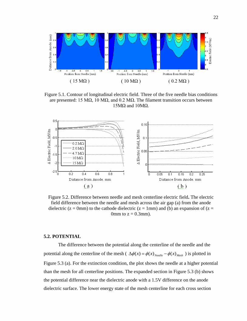
22
Figure 5.1. Contour of longitudinal electric field. Three of the five needle bias conditions
are presented: 15 MΩ, 10 MΩ, and 0.2 MΩ. The filament transition occurs between
15MΩ and 10MΩ.
Figure 5.2. Difference between needle and mesh centerline electric field. The electric
field difference between the needle and mesh across the air gap (a) from the anode
dielectric (z = 0mm) to the cathode dielectric (z = 1mm) and (b) an expansion of (z =
0mm to z = 0.3mm).
5.2. POTENTIAL
The difference between the potential along the centerline of the needle and the
potential along the centerline of the mesh ( MeshNeedle xxx )()()( ) is plotted in
Figure 5.3 (a). For the extinction condition, the plot shows the needle at a higher potential
than the mesh for all centerline positions. The expanded section in Figure 5.3 (b) shows
the potential difference near the dielectric anode with a 1.5V difference on the anode
dielectric surface. The lower energy state of the mesh centerline for each cross section
( 15 MΩ ) ( 10 MΩ ) ( 0.2 MΩ )

23
along the filament length means charge will flow perpendicularly from the needle
filament to the mesh filament dependent upon the conductivity of the path.
Figure 5.3. Difference between needle and mesh centerline potential. The voltage
difference between the needle and mesh across the air gap (a) from the anode dielectric (z
= 0mm) to the cathode dielectric (z = 1mm) and (b) an expansion of (z = 0mm to z =
0.2mm).
5.3. TRANSVERSE ELECTRIC FIELD
The transverse field (parallel to the dielectric surface), over the spatial cross-
section of Figure 5.1, applies a force to free charges that moves them towards or away
from the needle centerline. The transverse fields, positioned along the filament
centerlines at the anode dielectric surface, the centerline midpoint, and the cathode
dielectric surface for the 0.2-15MΩ conditions are shown in Figure 5.4. These plots
illustrate the voltage bias dependent change of the electric force directed between the
needle and mesh filaments. At the cathode dielectric surface, the needle and mesh
charges are isolated by the transverse force directing mesh and needle positive charges
towards their respective centerlines. At the cross-section of the centerline halfway point
and near the anode dielectric surface ( Figure 5.4, 0.5mm and 0.9mm ), the needle and
mesh charge is isolated by the transverse fields for conditions 0.2-10 MΩ. At the 15MΩ
condition, the needle transverse field relaxes near the cathode and reverses near the

24
anode. The resulting force draws negative charge on the anode towards the needle
filament position.
Figure 5.4. Transverse electric field as a function of x-position. The transverse electric
field which intersects the needle and mesh node positions at different distances away
from the anode dielectric for the range of bias conditions (0.2MΩ – 15MΩ).
The largest ratio of transverse field to longitudinal field for any point is 0.16
located at the cathode dielectric. Since the distance between the dielectrics ( 1.0 mm ) is
on the order of the distance between the needle and mesh position ( 0.88 mm ), the
movement of free charge in the gas volume is dominated by the 4.7-7.8 MV/m
longitudinal field with relatively little transverse movement along the filament. The
majority of lateral charge movement will occur on the charged dielectric surfaces where
the longitudinal force is balanced by the dielectric normal force. The transverse force
then dominates and has a compounding effect on the surface charge, which is present
beyond the period of the filament discharge. Since the transverse fields isolate the needle
and mesh charges present on the cathode dielectric surface, charge transfer between the
needle and mesh filaments is assumed to occur on the anode dielectric surface.
5.4. FREE SURFACE CHARGE LIMITATION
The charge density on the dielectric surfaces was estimated by the displacement
field, with units [C/m2] from the simulation. The displacement field and an integral form
of Gauss’s Law, Equation 8, were used to compare the dielectric surface charge at the
( 0.1 mm ) ( 0.5 mm ) ( 0.9 mm )
25
needle with the surface charge at the mesh. At the interface of the two mediums, Gauss’s
Law can be simplified to Equation 9 46
so that the difference between the normal
components of the dielectric ( and air ( equal the surface charge ( . The surface
charge is assumed to build up during discharge on the dielectric until it reduces the
electric field across the gas gap to below the dielectric strength of air ( ).
Equation 10 is then used to determine the respective needle and mesh surface charge
from the simulation data.
VS
xddanD 3
(8)
nDD aird
)( (9)
airairod ED (10)
The surface charges on the cathode dielectric surface at the needle and mesh
locations were estimated by taking the surface integrals. The areas of integration were
selected by using the areas which fell within a minimum field value over the needle and
mesh positions. The distribution of charge at 0.2MΩ is plotted in Figure 5.5 with the
integration area for 0.2MΩ condition outlined. The ratios shown in Figure 5.6 of the
needle to mesh charge vary by < 5% for different minimum field values selected with the
condition that they do not eliminate or combine the needle and mesh areas. At the
filament extinction condition the charge at the needle and mesh are equal.

26
Figure 5.5. Contour map of the displacement field on the cathode dielectric surface, at
0.2MΩ. Representative of the distribution of the charge on the dielectric surface. The
black outlines are the perimeter of the integration areas.
Figure 5.6. Ratio of needle to mesh charge, on the cathode dielectric. Charge calculated
from the displacement field charge distribution.
The same analysis was not conducted on the anode dielectric since the charge
distribution varies by 1% at the 0.2MΩ condition and <0.01% for the 15MΩ condition.
Charge distributions on the anode dielectric surface are assumed to be independent of
longitudinal field distribution and not inhibit transverse movement of surface charge.
0 5 10 15
1
1.2
1.4
1.6
1.8
2
Resistance, M
Ch
arg
e R
ati
o

27
6. DISCUSSION
In the context of the previously discussed filament formation physics, the field
changes are used to explain the experimental results of the light intensity. At the 15MΩ
condition, light intensity measurements give evidence that no filament forms at the
needle position. The measured needle voltage biases of the 475V and 560V for the
respective 6.5kV and 7.5kV driving voltages do not bring the electric field below the
dielectric strength of air. The charge that would otherwise travel through the filament
must be redistributed to offset the field forming along the centerline above the needle to
prevent a filament from forming.
6.1. FILAMENT EXTINGUISHING MECHANISM
At the 15MΩ condition the potential at all positions along the mesh centerline is
lower than the respective positions along the needle centerline. Considering the filament
is highly conductive along its length, this puts the entire filament as a whole at a higher
potential than the mesh filament. The transverse electric field on the cathode dielectric
surface prevents the surface charge on the cathode from moving between filaments. The
transverse electric field along the gas gap is < 16% of the longitudinal field and does not
have time to significantly affect the charge distribution within the air gap. The transverse
electric field on the anode transitions at the 15MΩ from positive to negative, reversing
the current of surface charge. The uniformity of the charge density on the anode with
variation of 1% - 0.01% create a uniform surface resistance. Charge transfer between the
two filaments can only appreciably occur on the anode dielectric surface, the dielectric
furthest from the needle electrode.
With constant surface resistance, surface current between the mesh and needle is
related to the surface voltage difference between the two positions. For the 0.2MΩ –
4.7MΩ conditions, the potential difference ( ), shown in Figure
6.1, is negative so that the current is directed towards the needle. This directs the
electrons from the filament at the needle away from the needle position. Increased needle
bias decreases the potential difference between the needle and the mesh position. This
decreases the flow of electrons from the needle position to the mesh position on the

28
anode. At 10MΩ the potential difference is zero and no electrons travel from the needle
position to the mesh position. At 15MΩ the current becomes negative. Positive charge
moves away from the needle position on the anode dielectric and the electrons from the
mesh position move towards the needle position. The surface charge transfer displaces
the field along the needle centerline so that the gas breakdown does not occur.
Figure 6.1. Potential difference between the needle and mesh on the anode dielectric
surface. The potential difference is representative of the negative surface current (electron
flow) directed from the mesh to the needle.
For the reversed polarity of the driving voltage, the electric field magnitude
remains the same but the directions switches. The charge movement still occurs on the
anode dielectric but with a reversed current direction. Surface electrons move away from
the needle centerline towards the mesh centerline to transfer across the gas gap through
one of the mesh filaments.
6.2. LIGHT INTENSITY RELATIONSHIP
The relationship between the modeled field values and measured light intensity
originates from Equation 11,47-49
the instantaneous light intensity flux rate ( ) equal to
the excitation flux rate (number of electron ionizations per cross-sectional area per time).
),(),(),(),( txutxntxtx ee (11)
0 5 10 15-5
-4
-3
-2
-1
0
1
2
Resistance, M
P
ote
nti
al,
V

29
Since the light of the discharge was recorded along the axis of the filament and over a
time period (125 ms) far greater than the discharge cycle (~200ns), 45
the total light
intensity is the time and space integral of the instantaneous light intensity, as expressed in
Equation 12.
dtdxtxutxntxT L
ee ),(),(),( (12)
The electric field oscillation has a period of 312.5μs so the applied electric field is
assumed constant for the period of time when the filament is producing light. The
electrons constitute the initial current charge carriers, when the majority of the current
and light emission occurs in the first ~20ns.47
The light intensity from a single discharge
is approximated as an instantaneous delta function where the value for is considered
constant with respect to time and obtained from the initial discharge field values.
The electron number density and the drift velocity can be combined in the
electron current density, as shown in Equation 13.
e
Jun e
ee (13)
The time integral of the current density results in the surface charge over the cross-
section of the filament, Equation 14.
T
es dttxJq ),( (14)
The radius of the filament is dependent upon the applied voltage and pressure, so it is
assumed constant across the gap as well as between the needle and the mesh filaments.38
The surface charge is then just a constant in the line integral along the filament and
represents the total electron charge (majority of the initial transferred charge) that passes
across the filament. The ratio of the light intensities can then be simplified to Equation 15

30
where the filament cross-sectional area is the same for both needle and mesh so that the
areas cancel. The light intensity flux areas also cancel since the same cross-section was
used for intensity sampling.
L
MM
L
NN
M
N
dxxq
dxxq
)(
)(
(15)
The first Townsend coefficient is integrated over the length of the gap using Equation 16
to relate the coefficient to the electric field.
E
Bp
pAex)( (16)
The first Townsend coefficient ( ) represents the number of ionzing electron-nuetral
collisions per unit distance as a function of E / p, defined by the empirical Equation 16.
The coefficient values A = 8.805 and B = 258.45, provided by a Sandia National
Laboratories Report,50
are curve-fits to a collection of literature data.
Due to the small variation between the electric fields, the ratios of the Townsend
coefficient are 1 ± 0.002 for each voltage bias condition. The light intensity variation, for
this approximation, is then solely dependent upon the total charge that crosses the air gap.
The charge ratio is compared to the light intensity in Figure 6.2. Since there is no
discharge at 15MΩ, the calculated surface charge is fixed to zero at 15MΩ while
maintaining the charge trend by subtracting the 15MΩ ratio value ~ (1:1) from the total
charge ratio. As justification, there will be a point at which a certain amount of charge
exists at the surface of dielectric but no discharge occurs. For this case, that occurs at the
1:1 ratio where charge competition eliminates the needle filament.
The assumption is supported by the results of Figure 6.2, where the calculated
trend of the light intensity falls along the average light intensity trends of the two
adjacent mesh nodes for 6.5kV and 9.0kV. The light intensity of the 7.5kV has a 160%

31
offset from the calculated values at 10MΩ but its initial and final values converge with all
sets of data. This trend may be due to additional surface charge built up across the
dielectric surface over areas of the mesh wire close to the dielectric but not at the mesh
node. The agreement of the calculated data and the cleaner filament data, at 6.5kV and
9.0kV, suggests that the trend of light intensity can be correlated with the electron charge
transferred.
Figure 6.2. Calculated and measured light intensity as a function of resistance. The
averaged light intensity values of the two adjacent filaments for 6.5kV, 7.5kV, and 9.0kV
are compared to the simulation surface charge ratio of the needle filament to the adjacent
filament. The calculated value assumes no intensity at 15MΩ, setting the trend of the total
charge to zero.

32
7. CONCLUSION
The data presented demonstrates the capability of a voltage biased by a resistive
load applied to an individual electrode to turn on and off a single filament while adjacent
to other discharging filaments in a DBD. The light intensity of the filament ranges from
~100% to 0% of the surrounding filaments intensities. Peak voltages of 476V and 560V
respective to the 6.5kV and 7.5kV driving voltages are required to completely turn off the
filament. However, lesser voltage changes of 100V can cause the observed transition
between a discharging filament and no filament. This relatively small change keeps the
voltage difference applied across the gas gap above the breakdown voltage for air. The
transition from discharge to no discharge at the needle is then dependent upon the space
charge interaction between the needle filament and its adjacent filaments.
The reverse of the self-bias process was demonstrated by applying a resistive load
to the mesh. The needle filament intensity doubled to 180% of the surrounding reference
filament intensity for a 470V bias rise applied to the mesh. The increased current
preference through the needle filament rerouted surrounding charge away from the mesh
node filaments which reduced their intensity to less than twice the ambient intensity
value.
The effect of built-up charge was investigated by comparing an acetone wiped
dielectric surface to a non-acetone treated surface for discharging. The acetone treatment
raised the required breakdown voltage and light intensity values. However, the light
intensity trend of the acetone treatment was consistent with the non-acetone treatment
and the filament transitioned to an off state between the same resistive values for both
treatments. The largest difference in voltage values was 10.4V (1.6% of the needle bias
voltage). The effect of cleaning the dielectric surface with acetone for each discharge was
determined to be negligible for this study.
Simulations of the field conditions for the biased needle produced trends with the
15MΩ extinguishing condition. The filament turns off when: 1) the electric field of the
needle is less than the field of the mesh at all respective points along the two filament
centerlines, 2) the charge at the needle and the mesh on the cathode dielectric are equal,
and 3) the transverse field between the needle and the mesh at the anode dielectric

33
creates a current from the needle to the mesh when the driving voltage polarity is positive
and a current from the mesh to the needle when the driving voltage polarity is negative.
These trends are associated with the movement and redistribution of charge particles,
specifically electrons, on the anode dielectric surface. Charge transferred from the mesh
filament displaces the field at the needle so that there is no breakdown at 15MΩ. Space
charge and cathode surface charge both have transverse fields that don’t allow
translational charge movement. The variation of the light intensity is related to the total
charge transferred across the air gap, represented by the surface charge at the needle. The
light intensity trend agrees with the shifted surface charge trend.
Control of a DBD filament intensity has been demonstrated by changing an
applied non-driving bias voltage by less than 7% of the driving voltage value, while the
filament was adjacent to other fixed filament discharges. This investigation also showed
that the voltage variation can affect other discharges beyond the immediately adjacent
filaments. The interaction between these filaments is determined by the charge interaction
on the dielectric with the uniform field distribution that allows charge to move between
filament positions.

34
BIBLIOGRAPHY
[1] Dong, L., Xiao, H., Fan, W., Zhao, H., and Yue, H. "A Plasma Photonic Crystal
With Tunable Lattice Constant," IEEE Transactions on Plasma Science Vol. 38,
No. 9, 2010, pp. 2486-2490.doi: 10.1109/TPS.2010.2055586
[2] Dong, L. F., Fan, W. L., Wang, S., Ji, Y. F., Liu, Z. W., and Chen, Q. "Pattern
formation in dielectric barrier discharges with different dielectric materials,"
Physics of Plasmas Vol. 18, No. 3, 2011, p. 033506.doi: 10.1063/1.3566003
[3] Wang, Y., Dong, L., Liu, W., He, Y., and Li, Y. "Generation of tunable plasma
photonic crystals in meshed dielectric barrier discharge," Physics of Plasmas Vol.
21, No. 7, 2014, p. 073505.doi: 10.1063/1.4889900
[4] Fan, W., Zhang, X., and Dong, L. "Two-dimensional plasma photonic crystals in
dielectric barrier discharge," Physics of Plasmas Vol. 17, No. 11, 2010, p.
113501.doi: 10.1063/1.3503625
[5] Dong, L., Li, B., Lu, N., Li, X., and Shen, Z. "Hexagonal superlattice pattern
consisting of colliding filament pairs in a dielectric barrier discharge," Physics of
Plasmas Vol. 19, No. 5, 2012, p. 052304.doi: 10.1063/1.4717466
[6] Sakaguchi, T., Sakai, O., and Tachibana, K. "Photonic bands in two-dimensional
microplasma arrays. II. Band gaps observed in millimeter and subterahertz
ranges," Journal of Applied Physics Vol. 101, No. 7, 2007, p. 073305. doi:
10.1063/1.2713940
[7] Sakai, O., Maeda, J., Shimomura, T., and Urabe, K. "Functional composites of
plasmas and metamaterials: Flexible waveguides, and variable attenuators with
controllable phase shifts)," Physics of Plasmas Vol. 20, No. 7, 2013, p.
073506.doi: 10.1063/1.4816698
[8] Sinclair, J., and Walhout, M. "Dielectric-Barrier Discharges in Two-Dimensional
Lattice Potentials," Physical Review Letters Vol. 108, No. 3, 2012, p.
035005.URL: http://link.aps.org/doi/10.1103/PhysRevLett.108.035005
[9] Osamu, S., and Kunihide, T. "Plasmas as metamaterials: a review," Plasma
Sources Science and Technology Vol. 21, No. 1, 2012, p. 013001.URL:
http://stacks.iop.org/0963-0252/21/i=1/a=013001
35
[10] Pendry, J. B., Holden, A. J., Stewart, W. J., and Youngs, I. "Extremely Low
Frequency Plasmons in Metallic Mesostructures," Physical Review Letters Vol.
76, No. 25, 1996, pp. 4773-4776.
URL:http://link.aps.org/doi/10.1103/PhysRevLett.76.4773
[11] Pendry, J. B., Holden, A. J., Robbins, D. J., and Stewart, W. J. "Magnetism from
conductors and enhanced nonlinear phenomena," IEEE Transactions on
Microwave Theory and Techniques Vol. 47, No. 11, 1999, pp. 2075-2084.doi:
10.1109/22.798002
[12] Zhang, H.F., Liu, S.B., and Li, B.X. "Investigation on the properties of
omnidirectional photonic band gaps in two-dimensional plasma photonic
crystals," Physics of Plasma No. 23, 2016, p.012105.
[13] Marr, G. V. Plasma spectroscopy. Amsterdam, New York [etc.] :: Elsevier Pub.
Co., 1968.
[14] Sakai, O., Shimomura, T., and Tachibana, K. "Negative refractive index designed
in a periodic composite of lossy microplasmas and microresonators," Physics of
Plasmas Vol. 17, No. 12, 2010, p. 123504.doi: 10.1063/1.3524561
[15] Naz, M., Ghaffar, A., Rehman, N., Shahid, S., and Shukrullah, S.
"Characterization of an In-house Built 50 Hz Single Dielectric Barrier Discharge
System Having Asymmetric Electrodes," International Journal of Engineering &
Technology IJET-IJENS Vol. 12, No. 05, 2012, pp. 53-60.
[16] Oliveri, G., Werner, D. H., and Massa, A. "Reconfigurable Electromagnetics
Through Metamaterials—A Review," Proceedings of the IEEE Vol. 103,
No. 7, 2015, pp. 1034-1056.doi: 10.1109/JPROC.2015.2394292
[17] Benford, J., and Swegle, J. High-Power Microwaves: Artech House, 1992.
[18] Liu, C.-H., Neher, J. D., Booske, J. H., and Behdad, N. "Investigating the
effective range of vacuum ultraviolet-mediated breakdown in high-power
microwave metamaterials," Journal of Applied Physics Vol. 116, No. 14, 2014, p.
143302.doi: 10.1063/1.4897219
[19] Seviour, R., Tan, Y. S., and Hopper, A. "Effects of high power on microwave
metamaterials," Advanced Electromagnetic Materials in Microwaves and Optics
(METAMATERIALS), 2014 8th International Congress on. 2014, pp. 142-144.

36
[20] Chien-Hao, L., Neher, J. D., Booske, J. H., and Behdad, N. "Investigating the
Physics of Simultaneous Breakdown Events in High-Power-Microwave (HPM)
Metamaterials With Multiresonant Unit Cells and Discrete Nonlinear Responses,"
IEEE Transactions on Plasma Science Vol. 42, No. 5, 2014, pp. 1255-1264.doi:
10.1109/TPS.2014.2313873
[21] Schamiloglu, E. "High power microwave sources and applications," Microwave
Symposium Digest, 2004 IEEE MTT-S International. Vol. 2, 2004, pp. 1001-1004
Vol.2.
[22] Manheimer, W. M., Fliflet, A. W., St. Germain, K., Linde, G. J., Cheung, W. J.,
Gregers-Hansen, V., Danly, B. G., and Ngo, M. T. "Initial cloud images with the
NRL high power 94 GHz WARLOC radar," Geophysical Research Letters Vol.
30, No. 3, 2003, pp. 1-4.doi: 10.1029/2002GL016507
[23] Kogelschatz, U. "Dielectric-Barrier Discharges: Their History, Discharge Physics,
and Industrial Applications," Plasma Chemistry and Plasma Processing Vol. 23,
No. 1, 2003, pp. 1-46.doi: 10.1023/a:1022470901385
[24] Valentin, I. G., and Gerhard, J. P. "Dynamics of dielectric barrier discharges in
different arrangements," Plasma Sources Science and Technology Vol. 21, No. 2,
2012, p. 024010.URL: http://stacks.iop.org/0963-0252/21/i=2/a=024010
[25] Dong, L., Shang, J., He, Y., Bai, Z., Liu, L., and Fan, W. "Collective vibration of
discharge current filaments in a self-organized pattern within a dielectric barrier
discharge," Physical Review E Vol. 85, No. 6, 2012, p. 066403.URL:
http://link.aps.org/doi/10.1103/PhysRevE.85.066403
[26] Kogelschatz, U. "Filamentary, patterned, and diffuse barrier discharges," IEEE
Transactions on Plasma Science Vol. 30, No. 4, 2002, pp. 1400-1408.doi:
10.1109/TPS.2002.804201
[27] Sakai, O., Sakaguchi, T., and Tachibana, K. "Photonic bands in two-dimensional
microplasma arrays. I. Theoretical derivation of band structures of
electromagnetic waves," Journal of Applied Physics Vol. 101, No. 7, 2007, p.
073304.doi: 10.1063/1.2713939
[28] Zhang, H.-F., Liu, S.-B., and Li, B.-X. "Investigation on the properties of
omnidirectional photonic band gaps in two-dimensional plasma photonic
crystals," Physics of Plasmas Vol. 23, No. 1, 2016, p. 012105.doi:
10.1063/1.4939540

37
[29] Zhang, H.-F., Ding, G.-W., Li, H.-M., and Liu, S.-B. "Complete photonic band
gaps and tunable self-collimation in the two-dimensional plasma photonic crystals
with a new structure," Physics of Plasmas Vol. 22, No. 2, 2015, p. 022105.doi:
10.1063/1.4906886
[30] Zhang, H.-F., Liu, S.-B., and Jiang, Y.-C. "Tunable all-angle negative refraction
and photonic band gaps in two-dimensional plasma photonic crystals with square-
like Archimedean lattices," Physics of Plasmas Vol. 21, No. 9, 2014, p.
092104.doi: 10.1063/1.4894213
[31] Park, W., and Wu, Q. "Negative effective permeability in metal cluster photonic
crystal," Solid State Communications Vol. 146, No. 5–6, 2008, pp. 221-227.doi:
10.1016/j.ssc.2007.10.042
[32] Wu, Q., and Park, W. "Negative index materials based on metal nanoclusters,"
Applied Physics Letters Vol. 92, No. 15, 2008, p. 153114.doi: 10.1063/1.2912529
[33] Eliasson, B., and Kogelschatz, U. "Nonequilibrium volume plasma chemical
processing," IEEE Transactions on Plasma Science Vol. 19, No. 6, 1991, pp.
1063-1077.doi: 10.1109/27.125031
[34] Lieberman, M. A. Principles of plasma discharges and materials processing.
Hoboken, N.J. :: Wiley-Interscience, 2005.
[35] Itikawa, Y. "Cross Sections for Electron Collisions with Nitrogen Molecules,"
Journal of Physical and Chemical Reference Data Vol. 35, No. 1, 2006, pp. 31-
53.doi: 10.1063/1.1937426
[36] Ryzko, H. "Drift velocity of electrons and ions in dry and humid air and in water
vapour," Proceedings of the Physical Society Vol. 85, No. 6, 1965, p. 1283.URL:
http://stacks.iop.org/0370-1328/85/i=6/a=327
[37] Gangwar, R. K., Levasseur, O., Naudé, N., Gherardi, N., Massines, F., Margot, J.,
and Stafford, L. "Determination of the electron temperature in plane-to-plane He
dielectric barrier discharges at atmospheric pressure," Plasma Sources Science
and Technology Vol. 25, No. 1, 2016, p. 015011.URL: http://stacks.iop.org/0963-
0252/25/i=1/a=015011
[38] Eliasson, B., Egli, W., and Kogelschatz, U. "Modelling of dielectric barrier
discharge chemistry," Pure and Applied Chemistry Vol. 66, No. 6, 1994, pp.
1275-1286.doi: 10.1351/pac199466061275

38
[39] Feng, Y., Ren, C. S., Nie, Q. Y., and Wang, D. Z. "Study on the Self-Organized
Pattern in an Atmospheric Pressure Dielectric Barrier Discharge Plasma Jet,"
IEEE Transactions on Plasma Science Vol. 38, No. 5, 2010, pp. 1061-1065.doi:
10.1109/TPS.2010.2043121
[40] Loeb, L. B., and Meek, J. M. "The Mechanism of Spark Discharge in Air at
Atmospheric Pressure. II," Journal of Applied Physics Vol. 11, No. 7, 1940, pp.
459-474.doi: 10.1063/1.1712796
[41] Meek, J. M., Craggs, J. D.,. "Electrical Breakdown of Gases," 1953.
[42] Emelyanov, O. A., and Shemet, M. V. "Single dielectric barrier discharge
characteristics in needle-to-plane configuration," Journal of Physics D: Applied
Physics Vol. 47, No. 31, 2014, p. 315201.URL: http://stacks.iop.org/0022-
3727/47/i=31/a=315201
[43] Xinxin, W., Haiyun, L., Zhuo, L., Ting, M., and Ruili, M. "Influence of wire
mesh electrodes on dielectric barrier discharge," Plasma Sources Science and
Technology Vol. 15, No. 4, 2006, p. 845.URL: http://stacks.iop.org/0963-
0252/15/i=4/a=030
[44] Qizheng, Y., Yunfei, W., Xingwang, L., Tian, C., and Guiwei, S. "Uniformity of
dielectric barrier discharges using mesh electrodes," Plasma Sources Science and
Technology Vol. 21, No. 6, 2012, p. 065008.URL: http://stacks.iop.org/0963-
0252/21/i=6/a=065008
[45] Kettlitz, M., Höft, H., Hoder, T., Reuter, S., Weltmann, K. D., and Brandenburg,
R. "On the spatio-temporal development of pulsed barrier discharges: influence of
duty cycle variation," Journal of Physics D: Applied Physics Vol. 45, No. 24,
2012, p. 245201.URL: http://stacks.iop.org/0022-3727/45/i=24/a=245201
[46] Jackson, J. D. Classical electrodynamics. New York, NY: Wiley, 1999.
[47] Morrow, R., and Lowke, J. J. "Streamer propagation in air," Journal of Physics D:
Applied Physics Vol. 30, No. 4, 1997, p. 614.URL: http://stacks.iop.org/0022-
3727/30/i=4/a=017
[48] Davies, A. J., Davies, C. S., and Evans, C. J. "Computer simulation of rapidly
developing gaseous discharges," Electrical Engineers, Proceedings of the
Institution of Vol. 118, No. 6, 1971, pp. 816-823.doi: 10.1049/piee.1971.0161

39
[49] Morrow, R. "Theory of negative corona in oxygen," Physical Review A Vol. 32,
No. 3, 1985, pp. 1799-1809.
URL:http://link.aps.org/doi/10.1103/PhysRevA.32.1799
[50] Warne, L., Jorgenson, R., Nicolaysen, S. "Ionization Coefficient Approach to
Modeling Breakdown in Nonuniform Geometries," Sandia National Laboratories
Vol. SAND2003-4078, 2003.

40
VITA
Matthew Crawford Paliwoda, attained his bachelor’s degree in aeronautical and
astronautical engineering from the University of Washington in 2012. There he
participated in plasma undergraduate student research with the ZaP Flow Z-Pinch
experiment. He then earned his master’s degree in aerospace engineering from Missouri
University of Science and Technology in July 2016, conducting graduate research with
the Aerospace Plasma Laboratory.

41