integration, the vlsi journalonline.sfsu.edu/mahmoodi/papers/paper_j28.pdf · domino logic designs...
TRANSCRIPT
INTEGRATION, the VLSI journal 46 (2013) 247–254
Contents lists available at SciVerse ScienceDirect
INTEGRATION, the VLSI journal
0167-92
http://d
n Corr
E-m
journal homepage: www.elsevier.com/locate/vlsi
Domino logic designs for high-performance andleakage-tolerant applications
Farshad Moradi a,n, Tuan Vu Cao b, Elena I. Vatajelu c, Ali Peiravi d, Hamid Mahmoodi e, Dag T. Wisland b
a Integrated Circuits and Electronics Lab, Department of Engineering, Aarhus University, Denmarkb Nanoelectronic Group, University of Oslo, Oslo, Norwayc Electronic Engineering Department, Universitat Polit�ecnica de Catalunya, Spaind Ferdowsi University of Mashhad, Irane NeCRL Group, Electrical and Computer Department, San Francisco State University, CA, USA
a r t i c l e i n f o
Article history:
Received 14 December 2011
Received in revised form
23 April 2012
Accepted 24 April 2012Available online 22 May 2012
Keywords:
Domino logic
FinFET
High-speed
Leakage
60/$ - see front matter & 2012 Elsevier B.V. A
x.doi.org/10.1016/j.vlsi.2012.04.005
esponding author. Tel.: þ45 4189 3344.
ail address: [email protected] (F. Moradi).
a b s t r a c t
Robustness of high fan-in domino circuits is degraded by technology scaling due to exponential
increase in leakage. In this paper, we propose several domino logic circuit techniques to improve the
robustness and performance along with leakage power. Lower total power consumption is achieved by
utilizing proposed techniques. According to the simulations in TSMC 65 nm CMOS process, the
proposed circuits increase noise immunity for wide OR gates by at least 3.5X and shows performance
improvement of up to 20% compared to conventional domino logic circuits. For FinFET simulation TCAD
tools have been used.
& 2012 Elsevier B.V. All rights reserved.
1. Introduction
High fan-in compact dynamic gates are often used in highperformance critical units of microprocessors. However, the useof wide dynamic gates is strongly affected by subthresholdleakage and noise sources [1]. This is mainly due to decreasedthreshold voltage that results in exponentially increased leakagecurrents in scaled technologies. To reduce power consumption,supply voltage scaling is used across technology scaling. However,threshold voltage needs to be scaled down as well to maintaintransistor overdrive for large ON currents. Less threshold voltagemeans smaller gate switching trip point in domino circuits.Smaller trip points make the domino circuit more prone to inputnoise. Moreover, excessive leakage can discharge the precharge(dynamic) node of a domino circuit resulting in a logic failure(wrong evaluation). In addition to reduced trip point andincreased leakage, other noise sources such as supply noise andcross talk noise also increase by technology scaling, furtherdegrading the robustness of domino logic [2–7].
A conventional approach to improve the robustness of dominocircuits is keeper transistor upsizing. However, as the keepertransistor is upsized, the contention between keeper transistorand NMOS evaluation network increases in the evaluation phase.
ll rights reserved.
Such current contention increases evaluation delay of the circuitand increases power dissipation. Thus, keeper upsizing trades offdelay and power to improve noise and leakage immunity. Suchtrade-off is not acceptable because it may make the circuit tooslow or too power hungry. There are techniques proposed in theliterature to address this issue. High speed domino logic [8] andconditional keeper [9] are among the most effective solutions forimproving the robustness of domino logic [10–14]. In this paper,we propose a new domino circuit for high fan-in and high-speedapplications in ultra-deep submicron technologies. The proposedcircuit employs a footer transistor that is initially OFF in theevaluation phase to reduce leakage and then turned ON tocomplete the evaluation. In order to avoid the delay penalty dueto an initially OFF footer transistor, an extra path for evaluation isprovided that is controlled by the output. According to simula-tions in a TSMC 65 nm process, the proposed circuit increasesnoise immunity by more than 26X for wide OR gates and showsperformance improvement of up to 20% compared to conven-tional domino logic circuits. The proposed circuit reduces thecontention between keeper transistor and NMOS evaluationtransistors at the beginning of evaluation phase. This results inless power dissipation for the proposed technique.
Aggressive device scaling has led to statistical variability indevice parameters and increased short channel effects (SCE)[15,16]. Thinner gate oxide helps to improve the short channeleffects. However, thinner gate oxide leads to exponentially highergate leakage.
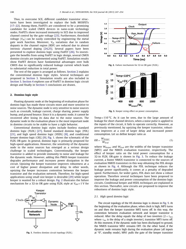
Fig. 2. Failure mechanism for 32-in OR gate (FLDL).
F. Moradi et al. / INTEGRATION, the VLSI journal 46 (2013) 247–254248
Thus, to overcome SCE, different candidate transistor struc-tures have been investigated to replace the bulk MOSFETs[17–22]. Among them, FinFETs are considered to be a promisingcandidate for scaled CMOS devices in nano-scale technologynodes. FinFETs show increased immunity to SCE due to improvedchannel control by the gate voltage [23]. Furthermore, thresholdvoltage (Vth) can be easily controlled by engineering the metalgate work function. Moreover, Vth variations due to randomdopants in the channel region (RDF) are reduced due to almostintrinsic channel doping [24,25]. Several papers have beenpresented to explore domino logic using FinFET [26]. To investi-gate the benefits from using FinFET in logic design, several CMOSdomino circuits are implemented using FinFET. Simulation resultsshow FinFET devices have fundamental advantages over bulkCMOS due to significantly reduced leakage current which leadsto substantial reduction in total power.
The rest of the paper is arranged as follows. Section 2 explainsthe conventional domino logic styles. Several techniques areproposed in Section 3. Simulation results are also included inSection 3. Section 4 explores use of FinFET in domino logic circuitdesign and finally in Section 5 conclusions are drawn.
Fig. 3. Keeper sizing effect on power consumption.
2. Domino logic style
Floating dynamic node at the beginning of evaluation phase fordomino logic has made these circuits more and more sensitive tonoise sources. The dynamic node is very sensitive to noise sourcessuch as crosstalk, leakage current, charge sharing, power supplybump, and ground bounce. Since it is a dynamic node, it cannot berecovered after losing its data due to the noise sources. Thedynamic node in the evaluation phase is the most important nodein domino circuits to be stable to have a right behavior.
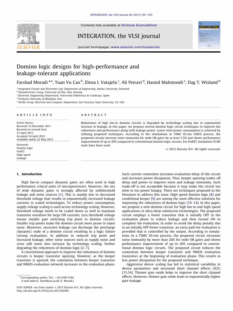
Conventional domino logic styles include footless standarddomino logic (FLDL) [27], footed standard domino logic (FDL)[21], and high speed domino logic (HSDL) [8], and conditionalkeeper domino logic (CKL) [9]. Fig. 1. shows the schematic of theFLDL OR-gate. In general, domino logic is primarily proposed forhigh-speed applications. However, the sensitivity of the dynamicnode to the noise sources has emerged as a serious designchallenge in scaled technologies. Conventionally, the keepertransistor is added to provide immunity to noise and leakage forthe dynamic node. However, adding this PMOS keeper transistordegrades performance and increases power dissipation in thecircuit. Upsizing the keeper transistor improves robustness at acost of higher power dissipation and delay. In other words,upsizing the keeper increases contention between the keepertransistor and the evaluation network. Therefore, for high-speedapplications using small size keeper is desirable [29] while largerkeeper is wanted for a robust design. Fig. 2 illustrates the failuremechanism for a 32-in OR gate using FLDL style at VDD¼1 V for
Fig. 1. Footless domino circuit topology (FLDL).
Temp¼110 oC. As it can be seen, due to the large amount ofleakage for short channel devices, when a noise pulse is applied tothe inputs of the circuit, it fails to operate correctly. However, aspreviously mentioned, by upsizing the keeper transistor, robust-ness improves at a cost of larger delay and increased powerconsumption. Let us define keeper ratio as
KR¼WKeeper
WEvalð1Þ
where WKeeper and WEval are the widths of the keeper transistor(MP2) and the NMOS evaluation transistor, respectively. Theeffect of keeper ratio on the total power consumption for a32-in FLDL OR-gate is shown in Fig. 3. To reduce the leakagecurrent, a footer NMOS transistor is connected to the sources ofevaluation NMOS transistors in this way obtaining the FDL designas shown in Fig. 4. Although the FDL technique reduces theleakage power significantly, it comes at a penalty of degradedspeed. Furthermore, for wider gates, FDL does not show a robustoperation. Therefore several techniques have been proposed toimprove the leakage and power consumption of the domino logiccircuits. Conditional keeper and HSDL techniques are explained inthis section. Thereafter, new circuits are proposed to improve therobustness of domino logic style.
2.1. High speed domino logic
The circuit topology of the HS domino logic is shown in Fig. 5. Atthe beginning of the evaluation phase, when clock is high, MP3 turnson and then the keeper transistor MP2 turns off. In this way, thecontention between evaluation network and keeper transistor isreduced. After the delay equals the delay of two inverters (2� tinv,where tinv is the delay of a single inverter), transistor MP3 turns off.At this moment, if the dynamic node has been discharged to ground,the NMOS transistor MN1 remains OFF. On the other hand, if thedynamic node remains high during the evaluation phase (all inputsat ‘‘0’’, standby mode), MN1 pulls the gate of the keeper transistor

Fig. 4. Footed domino logic style.
Fig. 5. HS Domino Logic topology.
Fig. 6. CKL logic circuit topology.
Fig. 7. Current-Mirror Footed Domino Logic schematic.
F. Moradi et al. / INTEGRATION, the VLSI journal 46 (2013) 247–254 249
to zero and turns on the keeper transistor to keep the dynamic nodehigh. However, since the keeper transistor is disabled, the dynamicnode is floating at the beginning of the evaluation phase. In presenceof large noise at inputs, the evaluation network discharges thedynamic node causing failure at the output of the circuit. Anotherproblem for HSDL is that the gate of keeper transistor MP2 can beVDD�Vth,MN1, where VtMN1 is the threshold voltage of the NMOStransistor MN1. Therefore, it results in a DC current through thePMOS keeper MP2 and the NMOS logic tree which increases the totalpower dissipation.
2.2. Conditional keeper logic
Another existing leakage-tolerant domino circuit is the conditionalkeeper domino logic (CKL) [9]. The circuit schematic of the condi-tional keeper is shown in Fig. 6. The circuit works as follows: at thebeginning of the evaluation phase, the smaller keeper (K1) turns on tokeep the state of the dynamic node. If the dynamic node is still high
after the delay equals the delay of two inverters, the output of theNAND gate goes low and turns on the transistor K2. This keepertransistor is sized larger than K1 to maintain the state of the dynamicnode for the rest of the evaluation period improving the robustness ofthe circuit. However, the conditional keeper K2 remains OFF whenthe dynamic node is discharged to the ground. The CKL design hassome drawbacks such as limitations on decreasing delays of theinverters and the NAND gate to improve noise immunity.
Although noise immunity can be ameliorated by upsizing thedelay inverters, it significantly increases power dissipation [8].Therefore, designing a leakage-tolerant and high performance circuitfor high fan-in application (e.g., Data path) is crucial. In the followingsection, several topologies are proposed to reduce power dissipationalong with improved robustness are proposed as follows:
a)
Current-Mirror Footed Domino Logic (CMFDL) b) High-Speed Clock-Delayed Domino Logic Style (HSCD) c) Modified HSCD (MHSCD) d) Conditional Evaluation Domino Logic (CEDL) e) Conditional Stacked Keeper Domino Logic (CSKDL)In this paper, NMOS evaluation transistors are referred asMeval.
3. Proposed domino logic circuits
3.1. Current-mirror-footed domino logic (CMF-domino)
The proposed leakage-tolerant circuit technique is illustrated inFig. 7 [10]. The transistor M7 is added to provide stacking effect toreduce leakage current during the evaluation phase. However,increased height of transistor stack in the evaluation path increasesthe evaluation delay. To reduce the evaluation delay, a currentmirror (M8) is added in parallel with the evaluation network toincrease the discharging current when at least one of the inputs ishigh. Transistor M9 provides a feedback from the output to the gatesof current mirror. This transistor connects the gates of currentmirror to ground when a dynamic node is discharged to ground.As a result, in presence of noises at inputs M9 helps to turn off thecurrent mirror and stops discharging the dynamic node. However,there is a trade-off between sizing of the mirror transistors andnoise immunity. In another word, by increasing the size of M8versus M7, noise immunity is degraded. The proposed circuit works

F. Moradi et al. / INTEGRATION, the VLSI journal 46 (2013) 247–254250
as follows: when the clock is low, the circuit is in the prechargemode, and the dynamic node (dyn-node) gets precharged to high.When the footer transistor (M6) is turned off a very small leakagecurrent passes through M7 pulling a negligible current from thedynamic node (dyn-node). In the evaluation phase when the clock ishigh, this circuit shows significantly improved noise immunity dueto the stacking effect provided by the transistor M7. When the clockis high, if all the inputs are zero, these three stacked NMOStransistors (Meval–M6–M7) substantially reduces the subthresholdcurrent. However, when at least one of the inputs switches to high,the mirror transistor pulls large current from the dynamic noderesulting in a high to low transition on the dynamic node. In thiscase, output of the gate goes high turning on the NMOS transistorM9 disabling the current mirror. For the rest of evaluation phasecurrent mirror remains OFF. Although a very high level of noise isapplied to the inputs of evaluation network, the proposed circuitworks properly as shown in Fig. 8. For these simulations, minimumsize keeper transistor is used to reduce the contention betweenevaluation network and keeper transistor.
3.2. High-speed clock-delayed domino logic style (HSCD)
Another proposed circuit topology is shown in Fig. 9 [11]. Theproposed circuit employs stacking effect (by adding the footertransistor MN1) to the tail of the evaluation NMOS tree for noiseimmunity improvement and uses the steady state voltage ofN-FOOT node at the beginning of evaluation phase to reduceleakage of the evaluation network. The operation of the circuit isexplained at different modes of operation.
3.2.1. Precharge mode
When clock is low, the circuit is in the precharge phase. MP1 isturned on and the dynamic node is charged to VDD. In addition,PMOS keeper transistor (MP2) is turned on helping the precharge.
Fig. 8. Simulation results for CMDL.
Fig. 9. High-speed clock-delayed domino logic style (HSCD) circuit.
At the beginning of the precharge phase, MN1 is ON, connectingthe N-FOOT node to ground. Furthermore, node GMN2 is low andMN2 is OFF. After the delay equals to the delay of the inverters(delay element), MN1 turns off. In this case, the voltage ofN-FOOT rises to an intermediate voltage level. The evaluationtransistors are sized such that the DC voltage on GMN2 node doesnot exceed the threshold voltage of MN2 to avoid any possibilityof short circuit current in the precharge phase. Transistor MN2 ischosen large to help the evaluation of the circuit.
3.2.2. All inputs at zero in evaluation
At the beginning of the evaluation phase, NMOS footertransistor MN1 is OFF which results in floated node N-FOOT.Therefore, N-FOOT node voltage reaches a DC value. Granted thatthis DC voltage exceeds 9Vtn�MP39þVOUT, transistor MP3 turns on.In other words
when VN-FootZVtp�MP3þVOUT )MP3 : ON ð2Þ
In that case, the GMN2 node is charged to VN-FOOT, therefore
VGMN2ZVtn�Mn2 )MN2 : ON ð3Þ
As a result, a wrong evaluation occurs. However, in theproposed HSCD technique transistors MN1, MN2, MP3, and MP4are sized in such a way that Eqs. (2) and (3) are not satisfiedavoiding any failure. Therefore, the DC voltage on node N-FOOTacts as a bias for the sources of transistors in evaluation networkwithout any effect on the functionality of the circuit. This DCvoltage reduces leakage of the evaluation network substantiallyresulting in significant leakage power reduction.
3.2.3. An input switching high
The waveforms of the circuit in this mode are shown in Fig. 10.As it is shown, the increased voltage on node N-FOOT at thebeginning of the evaluation phase turns on transistor MP3.Consequently, node GMN2 is charged to a voltage that is suppliedby N-FOOT node voltage. Therefore, GMN2 voltage goes higherthan the threshold voltage of MN2 depending on the sizing of thetransistors. Then NMOS transistor MN2 turns on at the onsetof evaluation phase (while the footer transistor MN1 is OFF),connecting the dynamic node to ground.
However the amount of this discharging current through MN2depends on the sizing of MN2 that has been selected largeenough. After a delay equals to the delay of two inverters,N-FOOT node is connected to ground and the rest of evaluationphase is accomplished through the footer transistor, MN1. There-fore, transistor MP3 switches off. When the dynamic node goeslow, the output node becomes high, turning on MN3 that leads toOFF MN2. However, the rest of evaluation phase (discharging ofthe dynamic node) completes through the evaluation networkand the footer transistor that is fully on. Here we have moredegree of freedom for increasing speed or enhancing noiseimmunity. For example, for improving speed, upsizing of MP3,MN2, MN1, evaluation transistors, and MN1 are all options.
Fig. 10. Waveforms for CWDL design.
F. Moradi et al. / INTEGRATION, the VLSI journal 46 (2013) 247–254 251
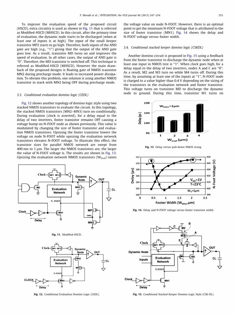
To improve the evaluation speed of the proposed circuit(HSCD), extra circuitry is used as shown in Fig. 11 that is referredas Modified-HSCD (MHSCD). In this circuit, after the primary timeof evaluation, the dynamic node starts to be discharged (when atleast one of inputs is at high). The input of the small keepertransistor MP2 starts to go high. Therefore, both inputs of the ANDgate are high (e.g., ‘‘1’’) giving that the output of the AND gategoes low. As a result, transistor MD turns on and improves thespeed of evaluation. In all other cases, the output of AND gate is‘‘0’’. Therefore, the MD transistor is switched off. This technique isreferred as Modified-HSCD (MHSCD). However the main draw-back of the proposed designs is floating gate of NMOS transistorMN2 during precharge mode. It leads to increased power dissipa-tion. To obviate this problem, one solution is using another NMOStransistor in stack with MN2 being OFF during precharge mode.
Fig. 13. Delay versus pull-down NMOS sizing.
3.3. Conditional evaluation domino logic (CEDL)
Fig. 12 shows another topology of domino logic style using twostacked NMOS transistors to evaluate the circuit. In this topology,the stacked NMOS transistors (MN2–MN3) turn on conditionally.During evaluation (clock is asserted), for a delay equal to thedelay of two inverters, footer transistor remains OFF causing avoltage bump on N-FOOT node as shown previously. This value ismodulated by changing the size of footer transistor and evalua-tion NMOS transistors. Upsizing the footer transistor lowers thevoltage on node N-FOOT while upsizing the evaluation networktransistors elevates N-FOOT voltage. To illustrate this effect, thetransistor sizes for parallel NMOS network are swept from400 nm to 1 mm. The larger the NMOS transistors are, the largerthe value of N-FOOT voltage is. The results are shown in Fig. 13.Upsizing the evaluation network NMOS transistors (WEval) raises
Fig. 11. Modified-HSCD.
Fig. 12. Conditional Evaluation Domino Logic (CEDL).
the voltage value on node N-FOOT. However, there is an optimalpoint to get the minimum N-FOOT voltage that is attributed to thesize of footer transistor (MN1). Fig. 14 shows the delay andN-FOOT voltage versus footer width.
3.4. Conditional stacked keeper domino logic (CSKDL)
Another domino circuit is proposed in Fig. 15 using a feedbackfrom the footer transistor to discharge the dynamic node when atleast one input in NMOS tree is ‘‘1’’. When clock goes high, for adelay equal to the delay of two inverters, nodes A and C are ‘‘0’’.As a result, M2 and M3 turn on while M4 turns off. During thistime, by assuming at least one of the inputs at ‘‘1’’, N-FOOT nodeis charged to a value higher than 0.4 V depending on the sizing ofthe transistors in the evaluation network and footer transistor.This voltage turns on transistor MD to discharge the dynamicnode to ground. During this time, transistor M1 turns on
Fig. 14. Delay and N-FOOT voltage versus footer transistor width.
Fig. 15. Conditional Stacked Keeper Domino Logic Style (CSK-DL).

Fig. 17. UNG versus Delay.
Table 1Power comparison for different circuit
techniques.
Circuit style Power (mW)
CMFDL 10.7
FDL 32.6
FLDL 88.9
CSKDL 12.3
HSCD 8.24
MHSCD 8.37
CKL 10.3
HSDL 22.5
CEDL 8.08
Fig. 18. Area comparison for proposed designs with standard domino techniques.
F. Moradi et al. / INTEGRATION, the VLSI journal 46 (2013) 247–254252
connecting node E to a high voltage (VDD�Vth). This leads to aweaker MP2 transistor that reduces the contention between MDand MP2. However, when node E holds a value higher thanVDD�Vth, transistor M1 helps to make MP2 stronger to improverobustness of the circuit. During this time M2 and M3 are ON. Thishelps to hold a high voltage at the gate of keeper transistor MP2.
After a delay equal to 2� tinv, by assuming low enough voltagelevel at dynamic node, M3 turns on while M2 remains ONconnecting node E to VDD. As a result MP2 turns off completelywhile transistor MN1 turns on at this moment (after 2� tinv) tospeed-up the evaluation process. Furthermore, the gate of M4connects to ‘‘1’’ with a drain and source connected to VDD.
After 4� tinv, M2 turns on, resulting in OFF path from VDD tonode E. At this time, transistor M4 keeps MP2 OFF for the rest ofevaluation phase. However, by assuming the circuit in standbymode (all inputs at ‘‘0’’), M4 connects the gate of MP2 to groundturning on the keeper transistor MP2 completely that helps tohold the dynamic node high. In this case, PMOS stacks are OFF.
The transistor MD plays a critical role to determine the speedof the circuit. However, upsizing the MD transistor lowers therobustness of the circuit. Fig. 16 shows the simulation results forCSKDL design. As it can be seen, the level of voltage at node E islowered to VDD�Vth due to using NMOS transistor (M1) connectedto the gate of keeper transistor. As a result, the current throughkeeper transistor increases resulting in improved robustness butalso in performance degradation.
To compare different topologies, we use Unity noise gain(UNG) metric to explore the robustness of the proposed circuits.The metric used in [30–33] is utilized to show the robustness ofdifferent topologies. A pulse noise is applied to all inputs withamplitude which is a fraction of supply voltage and a pulse widthequal to 20% of duty cycle. Then, the amplitude of the input noisepulse is increased until the amplitude of the resulting outputnoise voltage is equal to that of the input noise signal. This noiseamplitude is defined as
UNG¼ Vin,Vnoise ¼ VOutput ð4Þ
We simulated different topologies using TSMC 65 nm technol-ogy models. Simulation results are shown in Fig. 17. As it can beseen CMFDL shows significant improvement in robustness with apenalty of higher delay while MHCD style shows minimum delaycompared with other topologies. Although HS domino logic showsbetter delay compared to other topologies, it fails to operatecorrectly for high fan-in gates such as 16-OR gate during standbydue to high leakage through evaluation network. Among theproposed topologies, CEDL shows lower power consumptioncompared to other topologies. Table 1 shows the results atVDD¼1 V and Temp¼27 1C for CL¼100 fF.
The proposed circuits showed improved UNG compared to thestandard domino styles. However, to show a comprehensive
Fig. 16. CSKDL waveforms in evaluation mode.
comparison, the results for area (total Width� Length) are shownin Fig. 18. As it is shown, the CMFDL design is the smallest design atiso-UNG with an improved power consumption compared to otherdesigns.
4. FinFET domino logic circuit design
A FinFET device introduces significantly lower sub-thresholdand gate leakage current compared to bulk CMOS devices. This isattributed to a better controllability of the channel by two gates.The Drain-Induced Barrier Lowering (DIBL) is decreased due toreduced effect on the channel from drain and source terminals.Furthermore, fully-depleted channel helps to reduce randomdopant fluctuations significantly. As a result, using FinFET forhigh-performance applications is useful.

Fig. 19. FinFET FDL topology.
Fig. 20. Power comparison for FinFET and Bulk MOS.
F. Moradi et al. / INTEGRATION, the VLSI journal 46 (2013) 247–254 253
In this section, we implement domino logic circuit topologiesusing FinFET (Lg¼32 nm) to explore the benefits from utilizingFinFET in domino logic design. Fig. 19 shows the standard FinFETfooted-domino logic design including the corresponding wave-forms at different phases. FinFET domino logic affords betterperformance in a lower leakage power due to mitigated short-channel effect and a better controllability of the channel, wherethe results are shown in Fig. 20. The power comparison is underiso-delay for different circuits with a CL¼100 fF. The poweris measured as an average power drawn from the supply voltage.In this case all inputs are assumed at high considering the sizingto get minimum delay for each circuit technique.
Although FinFET devices have smaller channel length (32 nm),they show better noise immunity compared to 65 nm CMOStechnology. Furthermore, due to significantly reduced leakagecurrent through NMOS network, robustness of the FinFET imple-mentation improves significantly. However, implementing usingFinFET design suffers from discrete sizing of FinFET devices toachieve desired values of delay and power.
5. Conclusions
In this paper, several domino logic circuit topologies wereproposed for high-speed and leakage-tolerant design. Theproposed circuits showed at least 3.5X improvement in UNGcompared to the conventional design. Furthermore, FinFET based-Domino logic styles were simulated to investigate the advantagesfrom using FinFET in logic circuit design. Simulation results usingTCAD tools, Taurus, showed that FinFET domino logic designs
gives significantly lower leakage compared to utilizing bulk CMOSdevice. Simulation results show 2.7 times less power consump-tion of conventional domino circuit by using FinFET comparingwith USING Bulk CMOS devices.
References
[1] K. Roy, S. Mukhopadhyay, H. Mahmoodi, Leakage tolerant mechanisms andleakage reduction techniques in deep-submicron CMOS circuits, Proceedingsof the IEEE 91 (2003) 305–327.
[2] S.H. Choi, K. Roy, Domino noise model: a new crosstalk noise model fordynamic logic circuits, in: Proceedings IEEE International Conference SOC(Systems-on-Chip), 2003, pp. 207–210.
[3] H. Mostafa, M. Anis, M. Elmasry, Novel Timing Yield Improvement Circuits forHigh-Performance Low-Power Wide Fan-In Dynamic OR Gates, IEEE Transac-tions on Circuits and Systems I: Regular Papers 58 (8) (2011) 1785–1797.
[4] M. Alioto, G. Palumbo, M. Pennisi, Understanding the Effect of ProcessVariations on the Delay of Static and Domino Logic, IEEE Transactions onVery Large Scale Integration (VLSI) Systems 18 (5) (2010) 697–710.
[5] S. Weaver, B. Hershberg, N. Maghari, U.-K. Moon, Domino-logic-based ADCfor digital synthesis, IEEE Transactions on Circuits and Systems II: ExpressBriefs 58 (11) (2011) 744–747.
[6] C.H. Kim, K. Roy, S. Hsu, R. Krishnamurthy, S. Borkar, A process variationcompensating technique with an on-die leakage current sensor for nan-ometer scale dynamic circuits, IEEE Transactions on Very Large ScaleIntegration (VLSI) Systems 14 (6) (2006) 646–649.
[7] M. Anis, S. Areibi, M. Elmasry, design and optimization of multi-thresholdCMOS (MTCMOS) circuits, IEEE Transactions on Computer-Aided Design ofIntegrated Circuits and Systems 22 (10) (2003) 1324–1342.
[8] M.W. Allam, M.H. Anis, M.I. Elmasry, High speed dynamic logic style for scaled-down CMOS and MTCMOS technologies, in: Proceedings of the InternationalSymposium on Low Power Electronics and Design, 2000, pp. 155–160.
[9] A. Alvandpour, R.K. Krishnamurthy, K. Soumyanath, S.Y. Borkar, A sub-130-nmconditional keeper technique, IEEE Journal of Solid-State Circuits 37 (2002)633–638.
[10] F. Moradi, A. Peiravi, H. Mahmoodi, A new leakage tolerant for high fan-indomino gates, in: Proceeding of International Conference on Microelectro-nics, Tunisia, 2004, pp. 493–496.
[11] F. Moradi, H. Mahmoodi, A. Peiravi, A high speed and leakage-tolerantdomino logic for high fan-in gates, in: Proceeding of the 15th ACM GreatLakes Symposium on VLSI, (GLSVLSI), Chicago, IL, USA, 2005, pp. 478–481.
[12] F. Frustaci, P. Corsonello, S. Perri, High-performance noise-tolerant circuit techni-ques for CMOS dynamic logic, IET Circuits Devices and Systems (2008) 537–548.
[13] O. Gonzalez-Diaz, M. Linares-Aranda, F. Mendoza-Hernandez, A comparisonbetween noise-immunity design techniques for dynamic logic gates,Midwest Symposium on Circuits and Systems 1 (2006) 484–488.
[14] H.F. Dadgour, K. Banerjee, A novel variation-tolerant keeper architecture forhigh-performance low-power wide fan-in dynamic or gates, IEEE Transac-tions on Very Large Scale Integration (VLSI) Systems 99 (2010) 1–12.
[15] International Technology Roadmap for Semiconductors, 2001.[16] K. Bernstein, D.J. Frank, A.E. Gattiker, W. Haensch, B.L. Ji, S.R. Nassif,
E.J. Nowak, D.J. Pearson, N.J. Rohrer, High-performance CMOS variability inthe 65-nm regime and beyond, IBM Journal of Research and Development 50(4/5) (2006) 433–449.
[17] N. Collaert, A.D. Keersgieter, A. Dixit, I. Ferain, L.-S. Lai, D. Lenoble, A. Mercha,A. Nackaerts, B.J. Pawlak, R. Rooyackers, T. Schulz, K.T. Sar, N.J. Son, M.J.H. VanDal, P. Verheyen, K. von Arnim, L. Witters, Meyer De, S. Biesemans,M. Jurczak, Multi-gate devices for the 32 nm technology node and beyond,in: Proceedings of the 37th European Solid State Device Research Conference,ESSDERC, 2007, pp. 143–146.

F. Moradi et al. / INTEGRATION, the V254
[18] K. Noda, T. Uchida, T. Tatsumi, T. Aoyama, K. Nakajima, H. Miyamoto,T. Hashimoto, I. Sasake, 0.1 pm delta-doped MOSFET using post-energyimplanting selective epitaxy, VLSI Symposium on VLSI Technology Digest ofTechnical Papers (1994) 19–20.
[19] R. Yan, A. Ourmazd, K. Lee, Scaling the Si MOSFET: from bulk to SO1 to bulk,IEEE Transactions on Electron Devices 39 (1992) 1704–1710.
[20] T. Hori, A 0.1 pm CMOS technology with tilt-implanted punchthrough stopper(TIPS), International Electron Devices Meeting Technical Digest (1994) 75–78.
[21] F. Assaderaghi, D. Sinitsky, S.A. Parke, J. Bokor, P. KO, C. Hu, A dynamic-threshold MOSFET for ultra-low voltage operation, Electron Devices MeetingTech. Digest (1994) 809–812.
[22] T. Tanaka, K. Suzuki, H. Horie, T. Sugii, Ultrafast operation of Vi/th adjustedpþnþdouble-gate SO1 MOSFET’s, IEEE Electron Device Letters 15 (10)(1994) 386–388.
[23] D. Hisamoto, W.-C. Lee, J. Kedzierski, H. Takeuchi, K. Asano, C. Kuo, T.-J. King,J. Bokor, C. Hu, A folded-channel MOSFET for deep-sub-tenth micron era,IEDM Technical Digest (1998) 1032–1034.
[24] K. Sunouchi, et al., A surrounding-gate transistor (SGT) cell for 64/256MhitDRAM’S, International Electron Devices Meeting Technical Digest (1990)23–26.
[25] Y. Taur, T.H. Ning, Fundamental of Modern VLSI Devices, Cambridge Uni-versity Press, New York, NY, USA, 2009.
[26] S.H. Rasouli, H.F. Dadgour, K. Endo, H. Koike, K. Banerjee, Design Optimizationof FinFET Domino Logic Considering the Width Quantization Property, IEEETransactions on Electron Devices 57 (11) (2010) 2934–2943.
[27] B.-Y. Tsui, L.-F. Chin, A comprehensive study of the FIBL of nanoscaleMOSFETs, IEEE Transactions on Electron Devices 51 (10) (2004) 1733–1735.
[29] A. Chandrakasan, et al., Design of high performance microprocessor circuit,IEEE Press, Piscataway, NJ, 2000.
[30] A. Peiravi, F. Moradi, Dag T. Wisland, Leakage tolerant, noise immune dominologic for circuit design in the ultra-deep submicron CMOS technology forhigh fan-in gates, Journal of Applied Sciences 9 (2010) (2009) 392–396.
[31] A. Peiravi, M. Asyaei, Robust low leakage controlled keeper by current-comparison domino for wide fan-in gates, Integration, the VLSI Journal(2012) 22–32.
[32] F. Moradi, Dag T. Wisland, H. Mahmoodi, T.V. Cao, High speed and leakage-tolerant domino circuits for high fan-in applications in 70 nm CMOStechnology, in: Proceedings the 7th International Caribbean Conference onDevices, Circuits and Systems, ICCDCS, 2008. pp. 1–5.
[33] F. Moradi, A. Peiravi, H. Mahmoodi, A novel leakage-tolerant domino logiccircuit with feedback from the footer transistor in ultra-deep submicron, in:Proceeding of IEEE MIXDES 2006, Poland, 2006, pp. 201–205.
Farshad Moradi received the B.S. degree in electricalengineering from Isfahan University of Technology,Isfahan, Iran, in 2001, the M.S. degree in electricalengineering from Ferdowsi University of Mashhad, Mash-had, Iran, in 2005, and the Ph.D. degree from theUniversity of Oslo, Oslo, Norway, in 2011. From 2006 to2008, he was a Senior Lecturer with Ilam University, Ilam,Iran. From 2009 to 2010, he visited the NanoelectronicLaboratory, Purdue University, West Lafayette, IN. He iscurrently an Assistant Professor with the IntegratedCircuit and Electronics Laboratory, Department of Engi-neering, Aarhus University, Aarhus, Denmark. His current
research interests include ultralow-power digital/memorycircuit/device design for low-power biomedicalapplications.Tuan-Vu Cao received M.S. degrees in Electronic Engi-neering from Ho Chi Minh City University of Technology,Viet Nam in 2005, and PhD degree in Analog/Mixed-signal IC design from University of Oslo in 2012.
From 2006 to 2008, he was a research fellow at System-on-a-chip Design Laboratory of Changwon NationalUniversity, South Korea with the research topics of DC–DC converters for DDI, BGR, OTP memory circuits. From2008 to 2012, he was with the Nanoelectronics group,University of Oslo as a research fellow working towardshis Ph.D. degree. In 2010 he was appointed visitingscholar at the ISN lab, UC San Diego, USA. Since February
2012, he has been with Department of Electronics andTelecommunications, Norwegian University of Science and Technology—NTNU as apostdoctoral fellow. Currently, he is working on analog/RF and mixed-signal designsfocusing on low power ADC circuits, BF SK transmitters.
Elena Ioana Vatajelu received her M.S. degree in Physics
LSI journal 46 (2013) 247–254
at Babes Bolyai University of Cluj Napoca, Romania in2004 and in Control Engineering at Technical Universityof Cluj Napoca, Romania in 2005 and her PhD degree inElectronic Engineering from Universitat Polit�ecnica deCatalunya, Spain in 2011. From 2004 to 2007 she was aresearch assistant with the Control Engineering Depart-ment at Technical University of Cluj Napoca and from2007 to 2011 she was with the Electronic EngineeringDepartment at Universitat Polit�ecnica de Catalunya, Spainworking towards her PhD degree.
Since March 2012, she has been with the Microelec-
tronics Department at LIRMM Montpellier, France as apost-doctoral research fellow. Her current research interests include memory devicerobustness/reliability analysis, simulation based verification/validation, process varia-bility aware testing and yield enhancement.
Ali Peiravi was born in Tehran, Iran, in 1955. Hereceived the B.S. degree in electrical engineering fromthe University of Pittsburgh in 1976, the M.S. degree inelectrical engineering from the University of Californiaat Berkeley in 1978 and the Ph.D. degree in electricalengineering from the University of California at Irvi-nein 1984. He served as a research assistant at theElectronics Research Laboratory in the University ofCalifornia at Berkeley from 1976 to 1978 and workedas a senior design engineer at Intersil from 1978 to1980 and at American Microsystems Inc. from 1980 to1981. He taught at the California State University at
Long Beach, California State University at Pomona andthe University of California at Irvine during the period 1980–1984. He has been afull time faculty member at the Ferdowsi University of Mashhad since 1984. Hismain areas of interest are system reliability, control systems, real time systemsand design of VLSI. He is currently an Associate Professor of electrical engineeringat the Ferdowsi University of Mashhad.
Hamid Mahmoodi received the B.S. degree in electricalengineering from Iran University of Science and Tech-nology, Tehran, Iran, in 1998, the M.S. degree in electricaland computer engineering from the University of Tehran,Tehran, in 2000, andthe Ph.D. degree in electrical andcomputer engineering from Purdue University, WestLafayette, IN, in 2005. He is currently an AssociateProfessor of electrical and computer engineering withthe School of Engineering, San Francisco State University,San Francisco, CA. His research interest includeslow-power, reliable, and high-performance circuit designfor nanoscale technologies. He has many publications in
journals and conferences and is the holder of five U.S.patents. Dr. Mahmoodi was a recipient of the 2008 SRC Inventor Recognition Award,the 2006 IEEE Circuits and Systems Society VLSI Transactions Best Paper Award, the2005 SRC Technical Excellence Award, and the Best Paper Award of the 2004International Conference on Computer Design. He is a technical program committeemember of the International Symposium on Low Power Electronics Design and theInternational Symposium on Quality Electronics Design.
Dag T. Wisland received the M.Sc. and Dr. Sc. degrees inelectrical engineering from the University of Oslo, Oslo,Norway, in 1996 and 2003, respectively. He is a cofounderand currently the CEO of the fabless semiconductorcompany Novelda AS, Oslo, and is also a part-timeAssociate Professor with the Nanoelectronics Group, Uni-versity of Oslo. From 2004 to 2008, he was heading theNanoelectronics Research Group, University of Oslo. Hiscurrent research interests include low-power analog/mixed signal CMOS design, ultrawideband radio, anddesign of ADC/DAC with a particular focus on delta–sigma data converters. In his research, he has focused
on conceptually new methods and topologies combinedwith low-power design.Dr. Wisland is a TC member of the IEEE CAS Society Analog Signal Processing and
Biomedical Circuits and Systems technical committees.