integrated photonics institute for manufacturing ... · integrated photonics institute for...
TRANSCRIPT
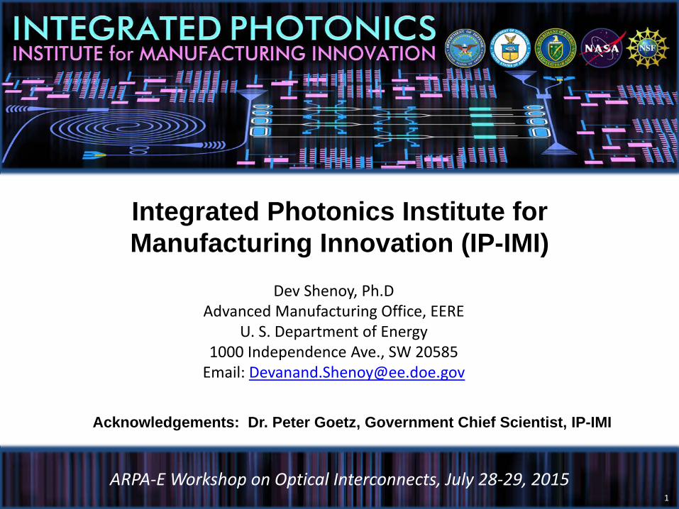
Integrated Photonics Institute for Manufacturing Innovation (IP-IMI)
Acknowledgements: Dr. Peter Goetz, Government Chief Scientist, IP-IMI
ARPA-E Workshop on Optical Interconnects, July 28-29, 2015
Dev Shenoy, Ph.DAdvanced Manufacturing Office, EERE
U. S. Department of Energy1000 Independence Ave., SW 20585
Email: [email protected]
1
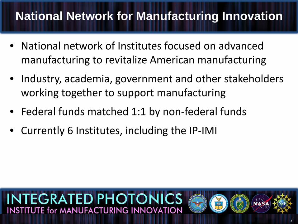
National Network for Manufacturing Innovation
• National network of Institutes focused on advanced manufacturing to revitalize American manufacturing
• Industry, academia, government and other stakeholders working together to support manufacturing
• Federal funds matched 1:1 by non-federal funds
• Currently 6 Institutes, including the IP-IMI
2
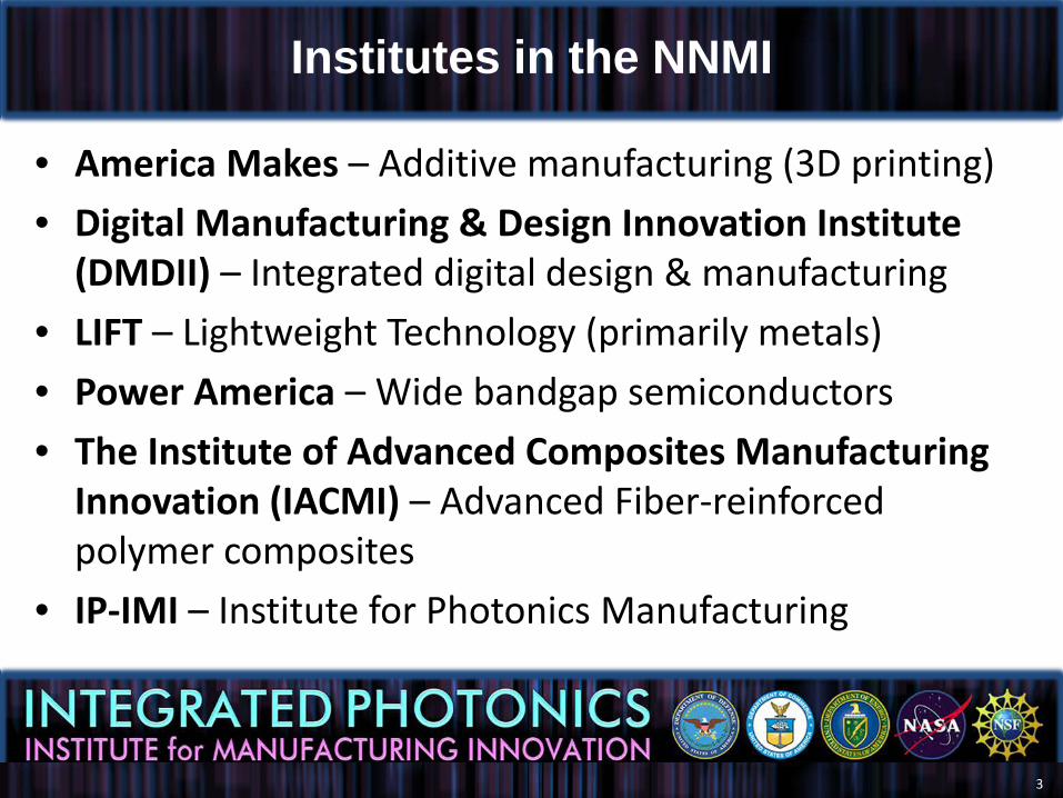
Institutes in the NNMI
• America Makes – Additive manufacturing (3D printing)• Digital Manufacturing & Design Innovation Institute
(DMDII) – Integrated digital design & manufacturing• LIFT – Lightweight Technology (primarily metals)• Power America – Wide bandgap semiconductors• The Institute of Advanced Composites Manufacturing
Innovation (IACMI) – Advanced Fiber-reinforced polymer composites
• IP-IMI – Institute for Photonics Manufacturing
3

IP-IMI Timeline
• October 3, 2014: President Obama announced the IP-IMI.
• November 5, 2014: AFRL released FOA on behalf of OSD/MIBP, requesting Concept Papers.
• December 19, 2014: Concept Papers due.• March 31, 2015: Full Proposals from Invited Proposers due.• July 28, 2015: Institute winner announced - RF-SUNY.• Institute’s operations will begin approximately January
2016. Federal funds run for 5 years.
4
Definition of Integrated Photonics
“Integrated photonics generally is the integration of multiple lithographically defined photonic and electronic components and devices (e.g. lasers, detectors, waveguides/passive structures, modulators, electronic controls and optical interconnects) on a single platform with nanometer-scale feature sizes.
5
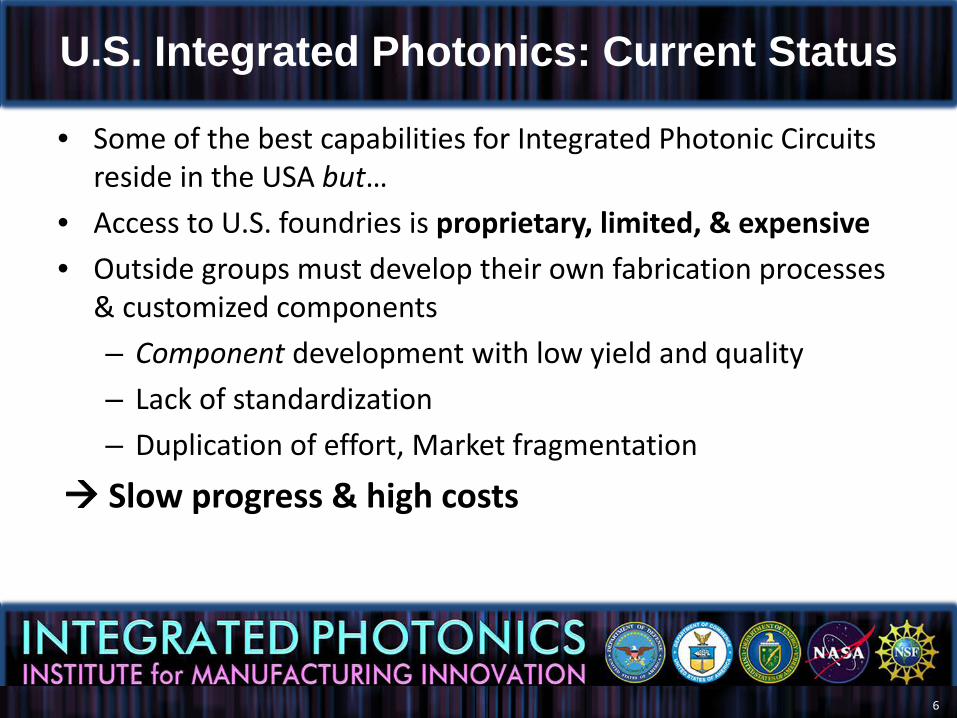
U.S. Integrated Photonics: Current Status
• Some of the best capabilities for Integrated Photonic Circuits reside in the USA but…
• Access to U.S. foundries is proprietary, limited, & expensive• Outside groups must develop their own fabrication processes
& customized components– Component development with low yield and quality– Lack of standardization– Duplication of effort, Market fragmentation
Slow progress & high costs
6
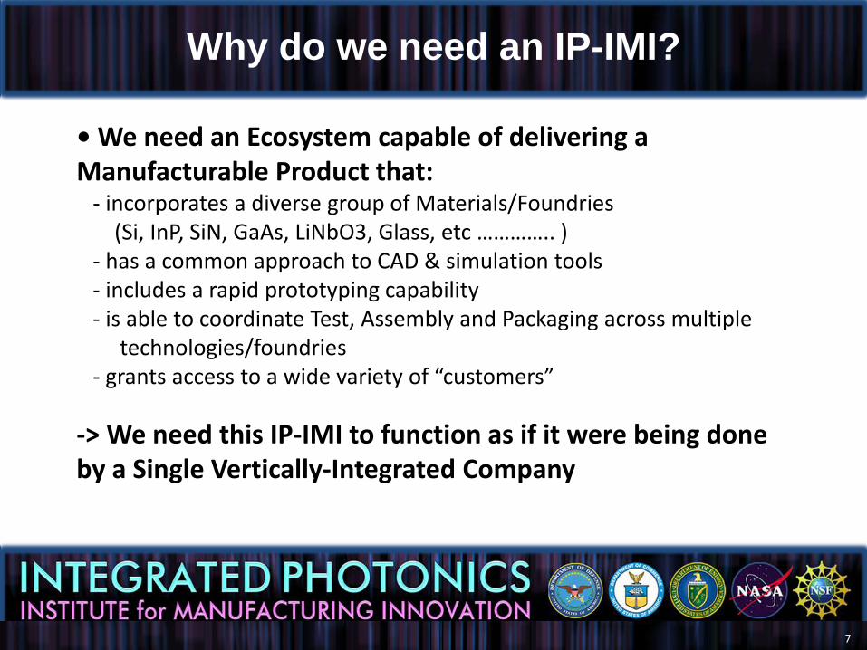
Why do we need an IP-IMI?
• We need an Ecosystem capable of delivering a Manufacturable Product that:
- incorporates a diverse group of Materials/Foundries (Si, InP, SiN, GaAs, LiNbO3, Glass, etc ………….. )
- has a common approach to CAD & simulation tools - includes a rapid prototyping capability- is able to coordinate Test, Assembly and Packaging across multiple
technologies/foundries- grants access to a wide variety of “customers”
-> We need this IP-IMI to function as if it were being done by a Single Vertically-Integrated Company
7
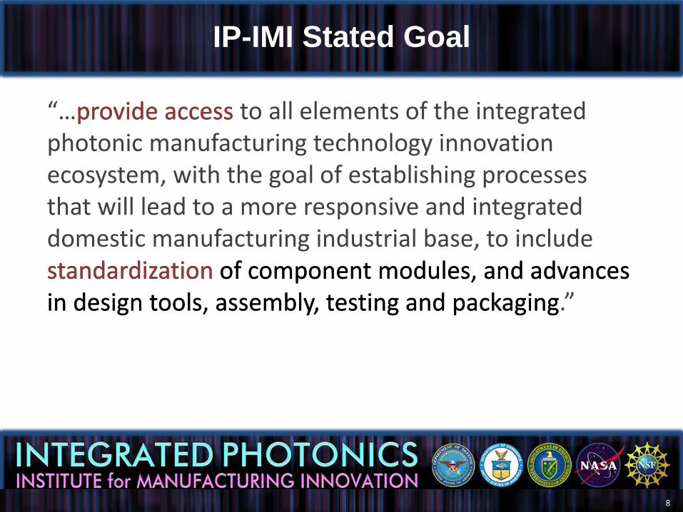
IP-IMI Stated Goal
“…provide access to all elements of the integrated photonic manufacturing technology innovation ecosystem, with the goal of establishing processes that will lead to a more responsive and integrated domestic manufacturing industrial base, to include standardization of component modules, and advances in design tools, assembly, testing and packaging.”standardization of component modules, and advances in design tools, assembly, testing and packaging
provide access
8
Integrated Electronics Solution: MOSIS
• MOSIS was built around 3 main ideas:– Standard building blocks for components & circuits– Share costs by putting multiple projects from various users
on a single mask set– Give government labs & universities access to foundries
“The Birth of the Microchip”http://www.longviewinstitute.org/projects/marketfundamentalism/microchip/“Funding a Revolution”http://ai.eecs.umich.edu/people/conway/Impact/FundingaRevolution.html
9
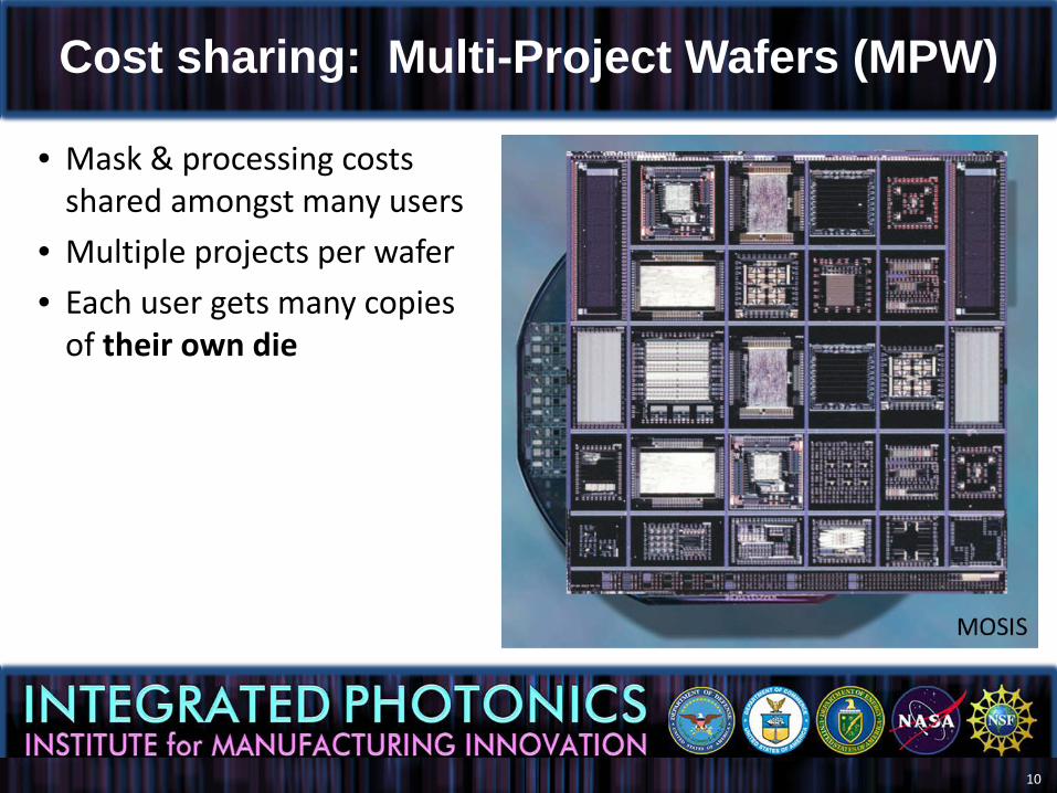
Cost sharing: Multi-Project Wafers (MPW)
• Mask & processing costs shared amongst many users
• Multiple projects per wafer• Each user gets many copies
of their own die
10
Impact of MOSIS on Electronics Industry
• Government labs, universities & small-to-medium enterprises (SMEs) have access to state-of-the art integrated electronics foundries
• Cooperation between academia & industry (uncommon prior to MOSIS)
• Academia provides industry w/graduates familiar with industry’s tools and techniques
• Greatly reduces costs of novel designs• Simplifies path to production, enabled fabless companies• Widely credited for helping U.S. regain its lead in
microelectronics
11
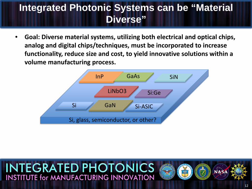
Integrated Photonic Systems can be “Material Diverse”
• Goal: Diverse material systems, utilizing both electrical and optical chips, analog and digital chips/techniques, must be incorporated to increase functionality, reduce size and cost, to yield innovative solutions within a volume manufacturing process.
InP
GaN
GaAs
LiNbO3 Si:Ge
Si, glass, semiconductor, or other?
Si-ASIC
SiN
Si
12

Electronic ICs Analogy to Photonic ICs
A
φ
P
resistor
capacitor
transistor
phase shifter
polarization converter
optical amplifier
Basic Electronic Elements Basic Photonic Elements
Electronic ICs are connected by metal traces
Photonic ICs are connected by waveguides
Devices are processed in parallel, creating Integrated Circuits
13
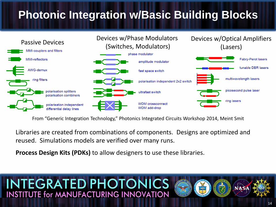
Photonic Integration w/Basic Building Blocks
Passive Devices Devices w/Phase Modulators (Switches, Modulators)
Devices w/Optical Amplifiers(Lasers)
Libraries are created from combinations of components. Designs are optimized and reused. Simulations models are verified over many runs.
From “Generic Integration Technology,” Photonics Integrated Circuits Workshop 2014, Meint Smit
Process Design Kits (PDKs) to allow designers to use these libraries.
14
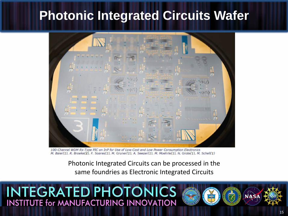
Photonic Integrated Circuits Wafer
Photonic Integrated Circuits can be processed in the same foundries as Electronic Integrated Circuits
15

Sample Integrated Photonic Circuits
JePPIX processed designs
16

Process Design Kits (PDKs)
17
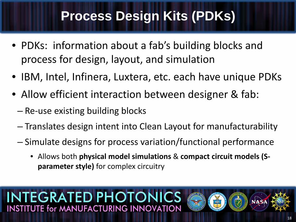
• PDKs: information about a fab’s building blocks and process for design, layout, and simulation
• IBM, Intel, Infinera, Luxtera, etc. each have unique PDKs• Allow efficient interaction between designer & fab:
– Re-use existing building blocks– Translates design intent into Clean Layout for manufacturability– Simulate designs for process variation/functional performance
• Allows both physical model simulations & compact circuit models (S-parameter style) for complex circuitry
Process Design Kits (PDKs)
18
Benefits of Using PDKs
• Reduces design time and cost• Allows complex designs to be successful on the 1st run
(Iteration could add a year!!!)• Allows Foundries to maintain proprietary designs (black
box components)• Simplifies porting designs from one foundry to another• Reduces level of education/training required to create
sophisticated designs• Gives easy access to standardized packaging
19
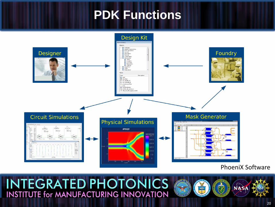
PDK Functions
PhoeniX Software
20
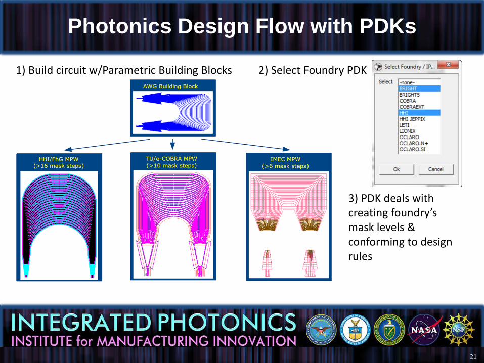
Photonics Design Flow with PDKs
1) Build circuit w/Parametric Building Blocks 2) Select Foundry PDK
3) PDK deals with creating foundry’s mask levels & conforming to design rules
21
What will the IP-IMI provide?
• Federal funding: $110 million (to be matched at least 1:1) • Access to world-class foundries and packaging houses
(both small-scale for research & large-scale for manufacturing)• Standardization of components, modules, assembly, testing,
and packaging• Packaging & Testing development for manufacturable products• Education & Training (Design training, Fab-resident training)
• Pool of educated designers creating new applications & companies, forming the basis for self-sustainment of the Institute
22
Standardization
+ Reduced design time & cost by eliminating need for re-designing basic components and packaging
+ Guaranteed functionality+ Increased 1st run success through decreased
process variations & validated simulations− Reduced flexibility, some designs not possible
Standardization is primarily addressed through PDKs
23
Collaboration and Membership
• Institute creates structure for competitors to pool resources and collaborate
• Membership provides legal framework for Intellectual Property management
24
IP-IMI Projects
25
3 Core Technical Areas Required
1. Digital data and communication links
2. Analog RF applications
3. Sensors (chemical, biological, and/or physical)
All of these should be producible at high volume. Packaging and Testing are critical!
26
Types of Institute Projects
The Institute will have 2 distinct types of projects:1. Project calls2. Customer projects
27
Project Calls
• Throughout the life of the Institute, research projects that support goals of the Institute will be solicited, selected, and awarded.
• These must provide benefit to the entire Institute Membership—not closed to other Institute Members
• Sharing of results & costs with the Institute is required• Publication of some results encouraged• Institute shares costs with Members
Awardee leads (w/Institute input)
28

Customer Projects
The Customer pays and leadsIncome helps support Institute
• Customers can be– Institute members– Non-members– Government agencies (e.g. DARPA)– Companies (large companies, SMEs, start-ups)
• Projects may include– Open projects (e.g. academic R&D)– Closed/proprietary projects– Mixed work (open and closed)
29
How do I Join a Project?
How other NNMI Institutes do Project Calls:• Project Call topic determined by Institute Leadership• If your organization is an Institute member, you will
be eligible to bid on project calls, typically as part of a team.
• If not an Institute member, you can team & propose as part of a team, but you can’t lead. You will be required to become a member if your team wins.
30