integrated distributed power management system for photovoltaic · 2014-10-01 · integrated...
TRANSCRIPT

Integrated Distributed Power Management
System for Photovoltaic
by
Edgar Martí-Arbona
A Dissertation Presented in Partial Fulfillment
of the Requirements for the Degree
Doctor of Philosophy
Approved July 2014 by the
Graduate Supervisory Committee:
Sayfe Kiaei, Chair
Bertan Bakkaloglu
Jennifer Kitchen
Jae-Sun Seo
ARIZONA STATE UNIVERSITY
August 2014
i
ABSTRACT
Photovoltaic (PV) systems are affected by converter losses, partial shading and
other mismatches in the panels. This dissertation introduces a sub-panel maximum power
point tracking (MPPT) architecture together with an integrated CMOS current sensor
circuit on a chip to reduce the mismatch effects, losses and increase the efficiency of the
PV system. The sub-panel MPPT increases the efficiency of the PV during the shading
and replaces the bypass diodes in the panels with an integrated MPPT and DC-DC
regulator. For the integrated MPPT and regulator, the research developed an integrated
standard CMOS low power and high common mode range Current-to-Digital Converter
(IDC) circuit and its application for DC-DC regulator and MPPT. The proposed charge
based CMOS switched-capacitor circuit directly digitizes the output current of the DC-
DC regulator without an analog-to-digital converter (ADC) and the need for high-voltage
process technology. Compared to the resistor based current-sensing methods that requires
current-to-voltage circuit, gain block and ADC, the proposed CMOS IDC is a low-power
efficient integrated circuit that achieves high resolution, lower complexity, and lower
power consumption. The IDC circuit is fabricated on a 0.7 m CMOS process, occupies
2mm x 2mm and consumes less than 27mW. The IDC circuit has been tested and used
for boost DC-DC regulator and MPPT for photo-voltaic system. The DC-DC converter
has an efficiency = 95%. The sub-module level power optimization improves the
output power of a shaded panel by up to 20%, compared to panel MPPT with bypass
diodes.

ii
DEDICATION
To my wife, for her comprehension, support and love.
I love you darling.
We finally made it!!!!
To my family, for their support and trust.

iii
ACKNOWLEDGMENTS
Special thanks to my wife Alix Rivera-Albino who was my companion and
support through every step of the way. I would like to thank Dr. Sayfe Kiaei and Dr.
Bakkaloglu for their continuous guidance, support and their invaluable help in the
development of this research. Thanks to my committee members Dr. Jennifer Kitchen
and Dr. Jae-Sun Seo. The invaluable help of James Laux was crucial in this work.
Finally, to Dr. Debashis Mandal, Chenxi Liu, Yao Zhao, Kiran Kumar Krishnan Achary
and Shrikant Singh who were always there when I needed them.

iv
TABLE OF CONTENTS
Page
LIST OF TABLES ............................................................................................................ vii
LIST OF FIGURES ......................................................................................................... viii
CHAPTER
1 INTRODUCTION .............................................................................................. 1
1.1 System Overview ........................................................................................ 1
1.2 Objectives ................................................................................................... 6
1.3 Summary of the Following Chapters .......................................................... 7
2 BACKGROUND ................................................................................................ 9
2.1 Photovoltaic Systems Architecture ............................................................. 9
Centralized PV System ............................................................................... 9
Distributed Power Management ............................................................... 15
Micro-Inverter ...................................................................................... 17
Parallel Power Optimizer ..................................................................... 17
Series Power Optimizer........................................................................ 18
Sub-Panel Power Optimizer ...................................................................... 19
Comparison of PV System Architectures ................................................. 20
2.2 Current Sensor .......................................................................................... 23
Resistive Current Sensor ........................................................................... 23
Current Transformer Sensor ..................................................................... 24
Hall Effect Current Sensor ........................................................................ 25
3 PROPOSED MPPT PHOTOVOLTAIC ARCHITECTURE ............................ 26

v
CHAPTER Page
3.1 Parallel Sub-Panel DC–DC Converter ...................................................... 26
3.2 Architecture of the Converter ................................................................... 28
3.3 System Specifications ............................................................................... 29
3.4 MPPT Converter ....................................................................................... 30
3.5 Output DC-DC Converter ......................................................................... 31
4 PROPOSED CURRENT SENSOR .................................................................. 33
4.1 Current to Digital Converter Operation .................................................... 37
4.2 Sensor Power Losses................................................................................. 40
5 CIRCUITS AND SIMULATION ..................................................................... 42
5.1 Photovoltaic Source .................................................................................. 42
5.2 DC-DC Converter ..................................................................................... 43
Converter Topology .................................................................................. 44
Converter Simulation ................................................................................ 45
5.3 CURRENT SENSOR CIRCUIT............................................................... 48
Sensor Front End....................................................................................... 50
Synchronous Comparator.......................................................................... 51
6 MEASUREMENTS AND ANALYSIS ............................................................ 56
6.1 Current Sensor Characterization ............................................................... 58
6.2 Indoor PV Test .......................................................................................... 63
6.3 Outdoor PV Test ....................................................................................... 68
7 CONCLUSIONS AND RECOMENDATIONS ............................................... 75
7.1. Conclusions ............................................................................................... 75

vi
CHAPTER Page
7.2. Recomendations ........................................................................................ 76
REFERENCES ................................................................................................................. 78

vii
LIST OF TABLES
Table Page
2-1 Power Loss and Recovered for Four PV System Architectures. .............................23
3-1 Distributed Sub-Panel DC-DC Converter Specifications. ......................................29
4-1 Comparison of Current Sensors for a Maximum Current of 830mA Sitting at
12V. .........................................................................................................................41
5-1 Characteristics of Two Parallel Panels. ...................................................................43
5-2 Sub-Panel System Specifications. ...........................................................................43
5-3 Components Values Calculated for Vin = 5V, V0 = 12V, Iin = 2A, and I0 =
0.83A .......................................................................................................................47
5-4 Specifications of the Current-to-Digital Converter Circuit. ....................................49
5-5 Component Values for the IDC Front End. .............................................................51
6-1 Specifications of the Prototype Boost Converter. ...................................................58

viii
LIST OF FIGURES
Figure Page
1-1 Residential Solar Power System. .............................................................................2
1-2 Block Diagram of a PV System. ..............................................................................2
1-3 PV System Basic Elements and Configuration. (a) Panel Configuration. (b)
Bypass Diodes Placement of Typical Commercial Product. ...................................3
1-4 Electrical Characteristics of a Mono-Crystalline PV Panel. (a) Typical
Current and Power as Function of the Voltage. (b) Response to Changes to
Incident Light (Irradiance). (c) Response to Changes in Temperature. ...................4
1-5 Perturb and Observe MPPT Algorithm....................................................................5
2-1 Block Diagram of a 4kW Residential PV System. The System Consists of
Two Strings in Parallel, Each with 11 Panels. .......................................................10
2-2 Block Diagram of an Inverter Box, Including the MPPT and the DC-AC ............11
2-3 Reconfigurable Photovoltaic Array Architecture. A Switch Network is Used
to Find the Configuration that Provides the Highest Power. .................................14
2-4 Distributed Converters. (a) Micro-Inverter. (b) Parallel Power Optimizer
(DC-DC). (c) Series Power Optimizer (DC-DC). .................................................15
2-5 Distributed Sub-Panel DC-DC with Centralized Inverter. (a) Single Panel
Configuration. (b) System Configuration. .............................................................20
2-6 Residential System Affected by Partial Shading. (a) Drawing of the Shaded
System. (b) Schematic View of the System. ..........................................................21
2-7 Example of I-V Curve for the System with the Centralized MPPT: (a) No
Shading and (b) Shaded Strings. ............................................................................22

ix
Figure Page
2-8 Resistive Current Sensor Block Diagram. .............................................................24
2-9 Current Transformer Sensor Block Diagram. ........................................................25
2-10 Hall Effect Current Sensor Block Diagram. ..........................................................25
3-1 Proposed Distributed Parallel Sub-Panel DC-DC Converter System. ...................27
3-2 Bypass Diodes in a Commercial Panel. The Figure Illustrates the Access
Points to Each Sub-Panel in a Commercial Panel. ................................................27
3-3 Internal Architecture of Distributed Sub-Panel DC-DC Converter. ......................28
3-4 Boost Double-Lift Converter for Sub-Panel MPPT...............................................30
3-5 Feed Forward Buck-Boost Converter. Partial Power Processing DC-DC
Converter Used for the Output Regulation. ...........................................................31
4-1 Block Diagrams of the Proposed Current Sensing. (a) Current Sensor. (b)
System. ...................................................................................................................33
4-2 Boost DC-DC Converter Timing Diagram. ...........................................................35
4-3 Sample Boost Output Waveform Characteristic. ...................................................36
4-4 AC Model of the IDC: (a) Switched Capacitor Sampling Circuit. (b)
Digitalization Circuit. ............................................................................................37
4-5 Timing Diagram of the Current Sensor (Not to Scale). .........................................38
5-1 I-V Curve for two Parallel Panels (Each Rated at 5V and 1A). ............................42
5-2 Boost Converter Circuit Schematic. ......................................................................44
5-3 Effect of Inductance. (a) Efficiency. (b) Input Current Ripple. (c) Match
Efficiency and Ripple at 10H. .............................................................................46
5-4 Output Parameters: (a) Maximum Voltage. (b) Maximum Current. .....................47

x
Figure Page
5-5 Transients Results of the Boost Converter Using the Values in Table 5.3. ...........48
5-6 Top Level Schematic of the Current Sensor. .........................................................49
5-7 Block Diagram of Comparator Used for the Current Sensor. ................................51
5-8 Latch Circuit with Pre-Amplification. ...................................................................53
5-9 Monte Carlo Simulation to Test the Offset of the Latch. The 3 Sigma Offset
is 64 mV. ................................................................................................................53
5-10 Pre-Amplifier Circuit Schematic. ..........................................................................54
5-11 Gain and Phase of the Pre-Amplifier. ....................................................................54
5-12 Instrumentation Amplifier Schematic. ...................................................................55
5-13 Monte Carlo Simulation to Test the Instrumentation Amplifier’s Offset. .............55
6-1 Prototype Board Used to Characterize the IDC IC and Test MPPT. (a)Block
Diagram of the Board. (b) Photo of the IDC IC. (c) Photo of the Board. ..............57
6-2 Measurement of the Offset of the Comparator. .....................................................59
6-3 Transient Measurement of the Current Sensor. (a) Voltage Ripple After the
DC Block Capacitor (2.5V Common Mode). (b) Sampling Signals (1 and
2). (c) Voltage on the Capacitors C1 and C2. (d) Output Signal of the
Comparator. ...........................................................................................................60
6-4 Response of the 8 Bits Counter Output due to Variation in Current. The
Figure Compares the Measured Results and the Values Estimated Using an
Ideal Output. ..........................................................................................................61
6-5 Measured IDC Performance. (a) DNL. (b) INL ....................................................62

xi
Figure Page
6-6 Power Dissipation of Current Sensor Using a 20 m Resistor Sensor and
the IDC (Note: y-Axis is in Logarithmic Scale). ...................................................63
6-7 Efficiency of the Boost DC-DC Converter. ...........................................................64
6-8 Setup Used for the Indoor MPPT Test. (a) Block Diagram of the System. (b)
Physical Setup. .......................................................................................................65
6-9 Test of the Output MPPT Algorithm Using the Proposed Current Sensor. ...........66
6-10 Indoor MPPT Test. (1) Panel Optimization. (b) Sub-Panel Level
Optimization. .........................................................................................................67
6-11 Measured Result of Indoor MPPT Test. (a) Panel Level Optimization. (b)
Sub-Panel Level Optimization. ..............................................................................68
6-12 Outdoor MPPT Test Setup. (a) Panels and Test Equipment. (b) Optimizer
Prototype Boards. ...................................................................................................68
6-13 Prototype Measurements Using Output MPPT Employing the IDC Sensor
Over Five Shading Cases. (a) I-V Curve. (b) Power vs. Voltage Curve. ..............69
6-14 Outdoor MPPT Test Setup. (a) Panel Level MPPT. (b) Sub-Panel Level
MPPT. ....................................................................................................................70
6-15 I-V Curve of the Three Sub-Panels. The Graphs Show the I-V Curves of the
Three Sub-Panels Under No Shade and Shade Conditions. ..................................71
6-16 Results of the Panel Level Optimization for all the Shading Patterns. (a) IV
Curve. (b) Power vs. Voltage Curve. .....................................................................72
6-17 Results of Optimization Under Partial Shading. (a) Panel Level
Optimization. (b) Sub-Panel Level Optimization. .................................................73

xii
Figure Page
6-18 Output Power for the Panel and Sub-Panel Optimization Systems for
Different Shading Patterns. (a) Comparison of Output Power. (b) Power as
Shading Increase in a Single Sub-Panel and Percentage of Improvement of
Sub-Panel vs. Panel MPPT. .................................................................................. 74

1
CHAPTER 1
INTRODUCTION
UE to the rising concerns about energy cost and environmental impact, along
with the depleting resources associated with fossil fuels, there is an increasing
demand on the development of alternative low-impact sustainable energy sources such as
photo-voltaic (PV), wind, hydro-electric and fuel cells. The PV source alternative
produces electricity in any location with direct sun light (even remote areas where utility
grid is not available), does not generate any noise (ideal for dense residential areas) and
requires low maintenance.
1.1 SYSTEM OVERVIEW
An example of a residential PV system is illustrated in Figure 1-1. Residential PV
power sources are considered small, with a power generation of less than 10kW [1], [2].
These power sources consist of:
Energy harvesting elements: array of PV panels,
Power management (PM) unit: used to maximize the power generation of
the PV array and convert from DC to AC power,
Distribution devices: junction box, meters, fuse, etc. used to direct the
power to the residence and electric utility grid [3].
The first two elements of the PV system can be represented in a block diagram as
shown in Figure 1-2. The PV generator, or array of panels, converts the incident light
(irradiance) to electric power. As part of the PM unit, the DC-DC converter is responsible
to track the maximum power point (MPP) of the PV panel/array to ensure the system is
D

2
working at its optimum point for any variation in irradiance, temperature or load. Finally,
an inverter is used to convert the DC power of the PV system to AC power. Once the
power is AC, it can be used to energize typical house appliances or connected it to the
utility grid.
Solar
E-Today= 2.0kWh
Solar
Solar
Converter
(Array)
Energy Source
Inverter
(MPPT and
Inversion)
Power
Distribution
Electric
Utility
Power
Use
Figure 1-1: Residential solar power system.
PV Array /
PV Module
DC-DC
Converter
(MPPT)
Inverter
AC
Output
Power
Optimized
DC Power
Figure 1-2: Block diagram of a PV system.
The basic unit of a PV system is the solar cells, as shown in Figure 1-3a. These
cells are pn-junction devices (diodes) that emit a high amount of current when exposed to
the sun light. In typical mono-crystalline photovoltaic panels, the cells produce a voltage

3
of 0.5 V and a current from 5 to 9 A. These cells are combined in series to increase the
output voltage in row called panels. A conventional mono-crystalline panel contains 72
cells in series to produce an output voltage of 36 V with a current of 5 to 9 A [4], [5]. The
panels contains bypass diodes every 24 cells to protect the cells against hot-spot [6], [7]
as illustrated in Figure 1-3b. This smaller group of 24 cells is called sub-panel.
+
0.5V
–
5A
Cell
5A +
36 V
–
72 C
ells
Panel
Panel
Symbol
5A+
12 V
–
...
24 C
ells
Sub-Panel
...
24
Cel
ls
Sub-Panel
Symbol
...
24
Cel
ls
...
24
Cel
ls
...
24
Cel
ls
(a)
+
12V
–
+
12V
–
+
12V
–
+
36V
–
...
24
Cel
ls
...
24
Cel
ls
...
24
Cel
ls
Commercial Panel Architecture
(b)
Figure 1-3: PV system basic elements and configuration. (a) Panel configuration. (b)
Bypass diodes placement of typical commercial product.
The current to voltage (I-V) characteristic of a PV panel is illustrated in Figure
1-4a. This I-V characteristic shows the fourth quadrant of an illuminated pn-junction
diode curve: as the voltage increases, the current will stay almost constant (similar to a

4
current source) until a specific voltage is reached where the current start falling
exponentially. Based on the I-V curve, the power of the PV panel is obtained as
illustrated in Figure 1-4a. The PV power characteristic shows a unique maximum power
point. This means that a specific load have to be connected to be able to operate the PV
panel at its maximum power point. Unfortunately, the IV curve varies with environmental
factors, such as incident light and temperature as shown in Figure 1-4b and c,
respectively. A different load is required to optimize the power for each light/temperature
condition. Real time optimization system is used to track the maximum power point of
the panel for any condition.
(a)
(b)
(c)
Figure 1-4: Electrical characteristics of a mono-crystalline PV panel. (a) Typical current
and power as function of the voltage. (b) Response to changes to incident light
(irradiance). (c) Response to changes in temperature.
The power maximization (MPPT) is achieved by combining a switched DC-DC
converter (buck, boost, buck-boost, etc.) and a maximum power point tracking (MPPT)
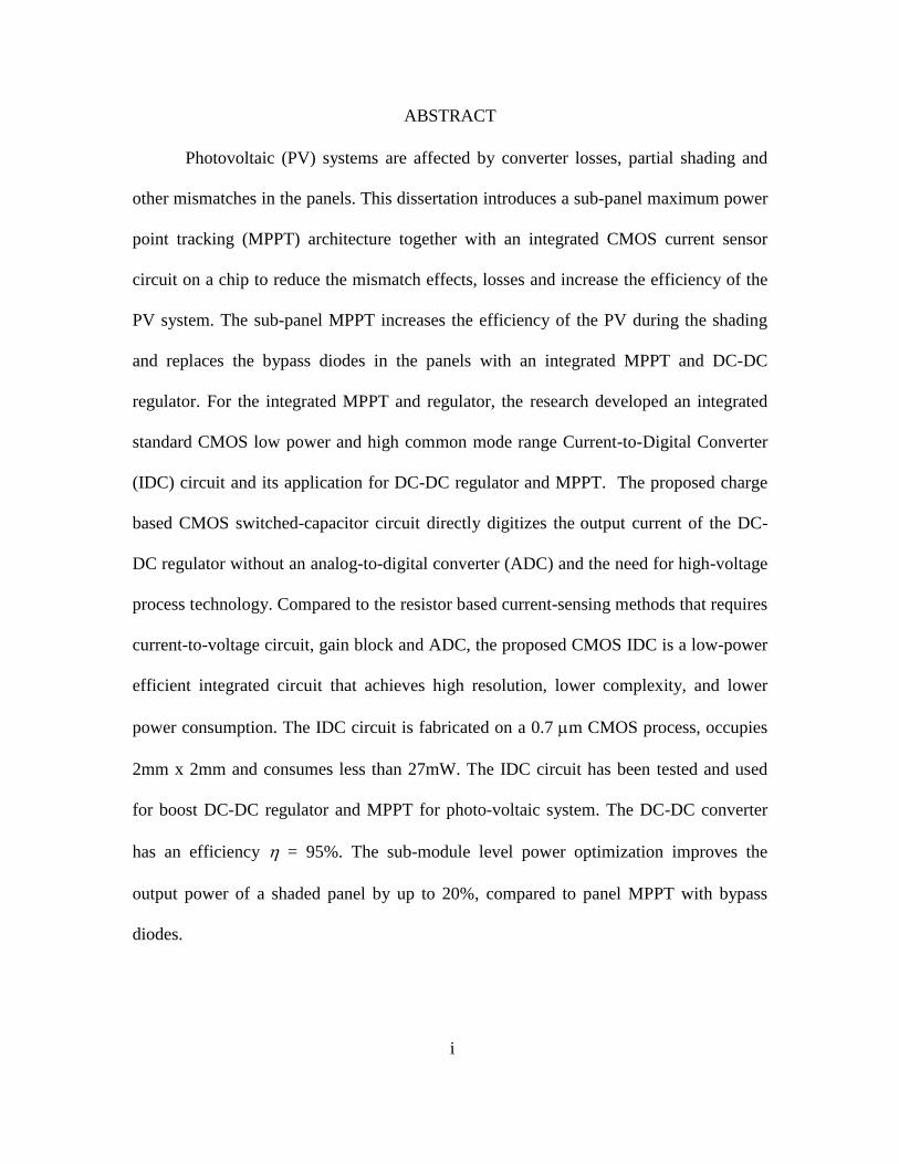
algorithm [3], [8-10]. Figure 1-5 illustrates the flow chart of one MPPT algorithm known
as perturb-and-observe (P&O). This algorithm uses a current and voltage sensor located
5
at the input of the DC-DC converter to calculate the generated power. Then, it determines
if the power is rising or falling compared to previous samples. With this information, the
conversion rate (e.g. duty-cycle, D) of the DC-DC converter is varied by a step size (ΔD).
This change results in variation of the input impedance of the converter (input current and
voltage change). The MPPT algorithm iterates to ensure the input impedance of the DC-
DC converter and the PV array match. The matching point is where the maximum power
is produced by the panel/array.
Start
READ
V(n) & I(n)
from sensors
Initialize
P(n–1) = 0
P(n) = V(n) · I(n)
P(n–1) = P(n)
V(n–1) = V(n)
ΔP > 0
ΔV < 0 ΔV < 0
D=D – ΔD D=D + ΔD D=D + ΔD D=D – ΔD
ΔP = P(n) – P(n–1)
ΔV=V(n) – V(n–1)
Yes
No No
No
YesYes
Figure 1-5: Perturb and observe MPPT algorithm.

6
An important step on MPPT for PV systems is the power sensing (voltage and
current sensing). The integration of voltage, current, or signal sensing (e.g. power-line
communication) is vital to enable improved performance and real-time stability. The
voltage is easy to measure, because most of the analog-to-digital converters (ADC) are
based on input voltage. On the other hand, current represents a challenge requiring either
lossy or large elements to convert current to voltage to then use an ADC. Given that the
DC current (power) in each PV panel is over several amperes (200-300W Power),
standard CMOS circuits cannot handle direct signal measurements. For PV application,
development of integrated circuits (IC) using standard CMOS technology will improve
size, efficiency, performance, reliability (minimum off-chip passive components), and
reduce the system cost [11], [12].
1.2 OBJECTIVES
In this research, a power management unit for residential or small commercial
solar systems is designed and implemented. The proposed system is aimed at improving
the current technology in photovoltaic power management units through the design of an
integrated current sensor using standard CMOS technology and a sub-panel distributed
converter. In order to achieve this goal, the following objectives must be fulfilled:
Reduce the system design complexity and size in an effort to make a simple
converter that can be integrated to the panels. This will make the system design
modular (single panel required for power increase), greatly simplified, and
smaller in size.

7
Minimize the use of passive and external components. This step will also help in
the reduction of the size of the converter. The use of state of the art FETs,
converters, and design techniques will allow this reduction.
Improve power extraction efficiency, converter availability (if a single converter
fails the reminder of the system is not affected), and MPPT (better response to
partial shading). The ability to perform MPPT at a sub-panel level improves the
power extraction and reduces the effects of partial shading and mismatches over
the panels. Having additional converters in the system reduces power outage
under converter failure by affecting only a small portion of the output power.
Reduce current sensing losses. Current sensing is a procedure that requires a
bulky coupling element or lossy passive element in series with the panels. This
research will use an alternate method that removes the series passive and coupling
elements, helping to improve the efficiency and size of the converter. The sensor
is designed in standard CMOS technology to minimize its size and the use of off-
chip components.
1.3 SUMMARY OF THE FOLLOWING CHAPTERS
This dissertation is organized as follows.
Chapter 2: Literature review. This chapter starts with the review of the common
PV architectures and a comparison between them. Then, it presents the typical
current sensing techniques used for photovoltaic applications.
Chapter 3: Proposed MPPT Photovoltaic Architecture. This chapter is devoted to
the high level PV architecture. It presents the block diagram of the proposed
system and gives an overview of the main blocks of the system.

8
Chapter 4: Proposed Current Sensor. This chapter introduces and explains the
proposed current sensor technique. It gives a detailed explanation of the proposed
current sensing technique as well as the high level of the circuit used in the
implementation.
Chapter 5: Circuits and Simulations. This chapter is devoted to the circuit
implementation and simulations used in the design process of the sub-panel
system and the current sensor. The first part gives the characteristics of PV panel
used for the design. Then, it contains the design of the DC-DC converter. Finally,
the details on the current sensor circuit are discussed.
Chapter 6: Measurements and Analysis. This chapter starts presenting and
describing the prototype. Then, the test goals and setup are explained. Finally, the
measured results and analysis of the proposed system are discussed.
Chapter 7: Conclusions and recommendations. This chapter provides the
conclusions and recommendations for future work.

9
CHAPTER 2
BACKGROUND
The objective of the MPPT systems is to optimize the output power of a PV
source [3], [8-10]. The output power that can be extracted from a PV system, under
mismatch conditions, depends on the type of MPPT architecture that is used and the
losses in the converters [1],[2]. This chapter will review and compare the system
architectures used for MPPT. Then, it will show the common current sensors used in PV
applications. This information will help on the development of specifications for the
system proposed in this research (PV architecture, DC-DC converter and sensor).
2.1 PHOTOVOLTAIC SYSTEMS ARCHITECTURE
The architecture employed for a PV system depends on the environment, location,
application, shape and size of the system. Typical PV systems for residential customers
produce power between 4kW to 10kW. These systems are commonly affected by
environmental factors such as shading, bird dropping and soiling [1],[2],[13-15]. This
section discusses and compares three PV power management architectures for residential
power sources: (1) centralized [3, 16, 17], (2) distributed panel level [13] [18-23] and (3)
sub-panel level [2, 24-28].
Centralized PV System
Residential photo-voltaic sources are commonly configured for centralized power
management. In a centralized PM system, the solar panels are configured in strings
(panels connected in series) to build the required voltage (e.g. ~ 400V for efficient DC-
AC conversion). Then, various strings are connected in parallel to get the desired power

10
level (e.g. 4kW to 10kW). Figure 2-1 shows the block diagram of a 4kW residential PV
system. The PV array is configured in strings of eleven panels to provide approximately
400Vdc at the input of the inverter (~ 2kW per string). The system contains two parallel
PV strings to achieve the desired power level (~ 4kW). Blocking diodes are added to each
string to avoid reverse current flow through the string under partial shading conditions
[3]. This combination of parallel strings is called PV array. The output power of the array
is then fed to the central PM unit for MPPT and DC-AC conversion [16, 17].
...
...
MPPT
400
V
+
–
+
120/240Vac
–
+
~36V_
11 P
V P
anel
Inverter
Figure 2-1: Block diagram of a 4kW residential PV system. The system consists of two
strings in parallel, each with 11 panels.
Figure 2-2 shows a block diagram of a central PM unit (inverter box). The
inverter box consists of two PM levels: (a) MPPT and (b) DC-AC conversion. The MPPT
is achieved by employing a DC-DC converter together with a maximization algorithm
controller. The controller senses the array power and decides the new converter’s duty
cycle to maximize the PV power. The output of the MPPT circuit is fed to an inverter to
convert the power from DC to AC. The AC output voltages amplitudes are 120Vac and
240Vac at a frequency of 60Hz (i.e. standard grid and household appliances voltage
levels in the United States).

11
E-Today= 2.0kWh
Solar
Input
Fil
ter
Outp
ut
Fil
ter
MPPT
Controller
Inversion/Phase
Control
PV Array
AC
Grid
Figure 2-2: Block diagram of an inverter box, including the MPPT and the DC-AC
The central system is the most intuitive architecture for photovoltaic systems, but
its performance could be limited. Some of the factors that affect the central power
management are: (a) components power stress (low reliability), (b) MPPT (partial
shading response), (c) fire and shock hazard and (d) system design complexity.
Details of the limitation of the central PM are as follow:
(a) Components power stress:
The central inverter box process the power of the entire array (4kW, in this
case). The components of this inverter must handle high voltage and current
levels under environments of high humidity and high temperature. To handle the
conversion rate and power levels, they normally require components such as
transformers and unreliable electrolytic capacitors [29]. Therefore, they occupies
a large area and suffer from a limited lifetime [29], [30]. The central inverter
represents 25% to 35% of the total cost of the system. On existing products, a PV
panel warranty is around 25 years, while, the warranty for a centralized inverter is
only 5 to 10 years[30]. This disadvantage requires to provide maintenance more
often to the system, replacing the inverter box up to five times in the life of the
solar panels.

12
(b) MPPT:
Photo-voltaic systems located in residences are exposed to different
environmental characteristics (i.e. trees, chimney, pipes, satellite dish, etc.). These
conditions cause mismatches due to clouds, partial shading, soiling, temperature
gradients, bird droppings, and physical degradation of the panel [1], [13-15]. The
mismatches degrade the performance of centralized inverter used in a residential
system by reducing the power yield in the operating points of the individual
panels [1],[2],[13-15]. Panels affected by mismatches in incident radiation or
temperature gradients does not allow other panel in the system to operate at their
maximum operating points, because they are limited by the series currents or
parallel voltages in the system. Bypass diodes are used to reduce this effect at the
expense of a reduction in the available power of the system (i.e., the power
generated by the shaded cells is not used).
(c) Fire and shock hazards:
The central PV system has to process the power of the entire array in a
single power management unit. There is not option of disconnecting or powering
down the array under any emergency (i.e. even if the inverter is OFF the array
still is energized). For example, in case of a fire, the array represents a shock
hazard to the fire fighters as well as any other person that throw water over the
panels (current flow through the water) [31]. Hazards also exist in any other type
of disaster where the emergency response people may be exposed to the array.

13
(d) System design complexity:
In a centralized design, the number of panels per strings, the brand, model
and orientation of the panels must be the same in the entire array. If a panel fails it
has to be replaced by the same brand and model, which may be difficult to find
after several years [13]. This configuration suffer from two limitations to increase
the power of the system after installation: (1) the inverter must be changed to
satisfy the new power level and (2) if the area where the system is installed does
not allow an entire new string, the system power cannot be increased (even if
there is space for some panels) [3].
In an effort to find the optimum power management for centralized PM systems,
academia has proposed reconfigurable arrays as shown in Figure 2-3 [32-36]. This
architecture combines the panels with a switch matrix that allow the reconfiguration of
the electrical path between individual panels in an array. The concept is to use the
information from each panel to search the configuration that provides the higher power.
Once the best configuration of the array is found the MPP is tracked by a centralized
converter.
Ideally, the reconfigurable concept provides great advantages to improve the
system performance under partial shading conditions. However, this architecture has
several limitations, such as:
(a) The switching matrix requires a high number of switches to be able to
configure the array.

14
Switch Network
. . .
. . .
. . .
.
.
.
MPPT+
120/240Vac
–
Inverter
.
.
.
Figure 2-3: Reconfigurable photovoltaic array architecture. A switch network is used to
find the configuration that provides the highest power.
(b) Driving the static switches represents a big challenge, because the gate voltage
required by all the switches is different and has to be independently
controlled.
(c) The losses introduced by the switches and extra wiring in the DC path degrade
the performance of the system.
(d) The status of all the panels has to be known to identify the shaded panels.
Iteration between configurations to find the higher MPPT slows down the
maximization process.
(e) The cost and complexity of the system is increased compared to the typical
centralized design.
All these problems results in a non-practical alternative for real time PV output power
maximization.

15
Distributed Power Management
Improvements in power electronics technology allowed relocating the power
management circuit from the central inverter box to the individual panels, as shown in
Figure 2-4. These single panel PMs are known as distributed MPPT converters
(DMPPT). Figure 2-4 presents the three more common DMPPT circuits: (a) micro-
inverter [13] [18-20], (b) parallel power optimizer [13] [21] and (c) series power
optimized [13], [22], [23]. Micro-inverters are DMPPT that maximize the power of the
panel and provides an AC output voltage (120Vac). The two optimizers (Figures b and c)
track the MPP at each panel and then use a simple central inverter for the DC-AC.
MPPT
...
+
~36V
-
120
Vac
+
-...
120Vac– +
MPPT
...
+
~36V
-
~400V
+
-
...400V – +
+120/240Vac
– (a) (b)
...
...
MPPT
. . .
. . .
. . .
400V
+120/240Vac
–
+
~36V
-
– +
(c)
Figure 2-4: Distributed converters. (a) Micro-inverter. (b) Parallel power optimizer (DC-
DC). (c) Series power optimizer (DC-DC).

16
DMPPT converters—either DC-DC converters or micro-inverters (DC-AC)—
provide many advantages over central PM. These advantages are: reduce power stress of
the components, additional power recovery, reduces system design constrains, individual
panel monitoring and diagnostics, and increase the availability of the system. DMPPT
circuits only process the power of a single panel (180W instead of 4kW). The reduced
power stress (voltage and current) on the components allows the replacement of
electrolytic capacitors and high voltage/current devices for more reliable parts. The use of
reliable parts allow companies to increase the warranties of these DMPPT circuits to
match the 25 years of the panels [37] [38].
Distributed converters are used to mitigate the effects generated by panel
mismatch and partial shading. This improvement is achieved by tracking the MPP of the
individual panels instead of the operating point of the entire array. There are several
models of DMPPT converters on the market [37] [38].
The distributed PM requires one converter per panel, increasing the system cost.
However, their use allows local maximization of the power (i.e., at the panel level).
Taking into account only partial shading mismatch, this method allows 11.8%
improvement to the annual output power, compared to the centralized PM [1] [2] [13].
Panel circuitry permits additional functions, such as, local monitor and diagnostic
of the system (fail detection). The communication with the individual panels also allows
the shutdown of the system under any emergency or disaster, reducing the shock hazard.
The next sub-sections will provide an overview of the available alternatives for
distributed power management including: (a) micro-inverter, (b) parallel power
optimizer, and (c) series power optimizer.

17
Micro-Inverter
One type of DMPPT circuit is the micro-inverter [13] [18-20]. This configuration
maximizes the power and provides an AC output voltage at each panel. Similar to the
central inverter box, this system uses a DC-DC converter for MPPT and a DC-AC
converter to obtain the AC output. One panel with a micro-inverter is a complete system
and can be used to power any AC load inside its power ratings.
Micro-inverters reduce the impact of a panel over the others and allows output
parallel connections, as shown in Figure 2-4a. The parallel connection of panels reduces
the design and planning of the PV system, because an arbitrary number of panels can be
connected to optimize the use of the available areas and client’s budget.
Micro-inverters are an ideal solution for systems that require a small amount
(<10) of panels (i.e. recreation vehicles, RV, or street lighting). As the system size
increases (i.e., residence requires >22 panels), the price also increases substantially. A
single micro-inverter costs 20% to 50% more than a power optimizer [39]. The increase
in the price is because each PM unit requires a DC-DC converter for MPPT and an
inverter for DC-AC. In addition, this topology requires phase detection and
synchronization between all the panels and with the utility power grid. This requirements
increase the complexity of the power quality control, sensing, and internal
communication.
Parallel Power Optimizer
Another alternative of DMPPT are the power optimizers (maximizers). The power
optimizers consist of a DC-DC converter per panel and a central inverter for the entire
array, as shown in Figure 2-4b and c. These power optimizers are divided in two main

18
groups based on the conversion rate and output connection required to achieve the
desired output voltage. We will refer to them as series and parallel power optimizers,
based on their output voltage connection.
Figure 2-4b shows the configuration of the parallel power optimizer architecture.
In this configuration, the converters maximize the output of the individual panels, and
boost the input voltage to achieve the required voltage for the inverter input (1:11 normal
conversion ratio). This technique allows parallel connection of the distributed PM units.
Similar to the micro-inverter case, the design of a parallel power optimizer provides the
flexibility to be adjusted to the available area and customer budget [13] [21]. In addition,
by increasing the output voltage, the current is decreased, allowing a reduction in the DC
wiring cost.
The high step-up ratio requires converter topologies that include transformers to
achieve the desired output voltage level [13], [21]. This causes an increase of the
converter size. In case of partial shading on the panel the bypass diodes short the shaded
portion of the panel resulting power lost, similar to the centralized case.
Series Power Optimizer
The series power optimizer architecture is shown in Figure 2-4c. This architecture
has a DC-DC converter per panel and a central inverter for the entire array, like the
parallel power optimized architecture. Similar to the connection of PV arrays for
centralizes systems, the output voltages of the converters are combined in series to build
up the voltage level required for the central inverter [13], [22], [23]. Therefore, in this
technique, the conversion rate of the DC-DC converters is small (commonly 1:1).

19
The series power optimizer provides single panel power optimization as well as
panel monitoring and control. The connection of the outputs in series causes a
dependency of output current on all the series-connected converters [13]. If just one
converter cannot provide the required current the others will be affected.
Series power optimizer adds complexity to the system design, because many
panels have to be connected in series to achieve the required voltage. If the customer
wants to increase the system power, an entire row has to be installed reducing the
flexibility to upgrade the system.
Sub-Panel Power Optimizer
The most recent development in DMPPT converters is the sub-panel power
optimizer. This architecture uses three DC-DC converters instead of bypass diodes
(avoiding the diodes to turn ON under partial shading), as shown in Figure 2-5a. The
converters are used to separately optimize the power of the sub-panels [2, 24-28]. This
topology is similar to the series power optimizer, but, in this case, the series converters
are internal to the panel.
The DC-DC converters used in published works produce low conversion rates
(i.e., 1:1, buck or buck-boost) [2, 24, 25]. The resulting output after the combination of
the three converters give the typical voltage of a panel (i.e., 36V), as shown in Figure
2-5a. Replacing the bypass diodes by sub-panel MPPT converter gives two main
advantages: (1) the power of a shaded sub-panel is optimized instead of bypassed and (2)
eliminate the multiple maximum power points under partial shading.
This architecture improves the energy production under partial shading by around
14.6%, compared to the centralized MPPT [1] [2]. The sub-panel power optimizer

20
architecture results in a reduction of power stress on each converter, improves the energy
production under partial shading and removes the local maximum power points allowing
simpler MPPT algorithms.
The combination of several panels in series, to achieve the voltage required for
the central inverter (Figure 2-5b), increases the design complexity and limits the
flexibility of the array.
...
24
Ce
lls
...
24
Ce
lls
...
24
Ce
lls
DC-DC Converter
(MPPT)
DC-DC Converter
(MPPT)
DC-DC Converter
(MPPT)
+12 V–
+12 V–
+12 V–
+12 V–
+
36 V
–
+12 V–
+12 V–
...
...
MPPT
. . .
. . .
. . .
400V
+120/240Vac
–
+
~36V
-
– +
(a) (b)
Figure 2-5: Distributed sub-panel DC-DC with centralized inverter. (a) Single panel
configuration. (b) System configuration.
Comparison of PV System Architectures
This section compares the three methods for PV power management discussed
above: central, distributed and sub-panel level. The study compares the three PV PM
architectures in the same system and shading circumstances. The comparison is based on
the residential system shown in Figure 2-6a.
21
11
111
111
11
1
22
222
222
22
2
(a)
MPPT
150 - 400V – +
+
120/240Vac
–
~36V– +
Inverter
11 PV Panel
(b)
Figure 2-6: Residential system affected by partial shading. (a) Drawing of the shaded
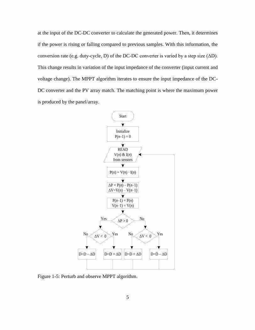
system. (b) Schematic view of the system.
The example consists of 22 PV panels (4kW) located on a residence roof with
elements such as chimney, pipes and satellite dish [40]. The case under study is at
3:00pm where shading reaches some of the panels producing partially shading. At that
time of the day the expected incident irradiance is 600kW/m2 and shaded irradiance is

22
200kW/m2 [1]. The analysis for the central power management system will be explained
in detail and the others methods wills be calculated similarly.
Figure 2-6b shows the panels connected in a centralized PV system configuration.
The system contains two rows (strings) of 11 panels each (396 V). When the two sub-
circuits (String 1 and String 2) are matched (no shading), they have a common maximum
power point, as shown in Figure 2-7a. When the system is exposed to shades (Figure
2-7b), the shaded sub-circuits operate at a different operating point. As result, the
combined maximum power point (1.7 kW) differs from the combined operating points of
the individual sub-circuits (0.82 kW + 1.069 kW = 1.89 kW).
(a) (b)
Figure 2-7: Example of I-V curve for the system with the centralized MPPT: (a) no
shading and (b) shaded strings.
Centralized power management suffers a power loss of 27% from the non-shaded
case. If the power of the individual strings is maximized, 11% of that power loss in
central PM can be recovered. Table 2-1 illustrates the power improvement for the
different levels of distributed MPPT. The sub-panel power optimization represents a
substantial power improvement with a 20% additional power. This makes it a viable
alternative for improved power maximization.

23
Table 2-1: Power loss and recovered for four PV system architectures.
MPPT Level Power
(kW)
Loss from no-shade
(%)
Improve from Central
(%)
Central 1.70 27.6 0.0
String 1.89 19.6 11
Panel 1.93 18.0 13.2
Sub-Panel 2.05 12.6 20.7
2.2 CURRENT SENSOR
Power metering for MPPT allows the PM unit to obtain the optimum power from
the solar panels. In power sensing, two quantities are required: voltage and current. The
voltage sensing can be easily obtained with ADCs. Current sensing is more challenging,
because there is not a direct method to sense current. The goal in this research is to find a
current sensor which is compact, easy to integrate to an integrated circuit (IC) and uses
standard CMOS even for high voltage levels. This section discusses three current sensing
alternatives for MPPT: (1) resistor, (2) Hall Effect, and (3) current transformer.
Resistive Current Sensor
The most common current sensing approach uses a series resistor to convert the
current into a voltage, and digitize the signal using an ADC as shown in Figure 2-8 [41-
48]. This method is simple to implement and consumes a small area compared to other
methods. The additional series resistance has several disadvantages in terms of
efficiency, accuracy, heat dissipation, and requires high voltage CMOS process.
A variant to this method is to replicate a scaled version of the current of the triode
device (switch). Then, the scaled current flows through a sensing resistor to be converted
to voltage [49],[50]. However, due to the high current that flows through the triode

24
device, external FETs are required. Therefore, this method is not a viable alternative for
high currents PV systems.
PV Array / Panel
DC-DC (Converter) Lo
ad
Rsense
+ -Substract/
Amp.
ADC Control(MPPT)
(I)
(D)
(V)
IPV
ADC
Figure 2-8: Resistive current sensor block diagram.
Current Transformer Sensor
The current transformer sensor is a better alternative for high current
environments [48, 51, 52]. This method used a 1:N current transformer to couple the
current to an isolated circuit in the secondary, as shown in Figure 2-9. This isolated
circuit converts the current into a voltage and digitize the value using an ADC. The
circuit in the secondary can now use standard CMOS process to digitize the signal.
However, a transformer in the signal path adds inductance to the path, increases the
noise, sensor size, electromagnetics emission, design complexity, and require additional
ADC circuit.

25
PV Array / Panel
DC-DC (Converter) Lo
ad
ADC Control(MPPT)
(I)
(D)
(V)
IPV
ADC
A
Rsense
Figure 2-9: Current transformer sensor block diagram.
Hall Effect Current Sensor
The Hall Effect current sensor uses a concept similar to the current transformer
[48, 51, 52]. The sensor couples the magnetic field produced by the current to a
piezoelectric material and a magnet. The secondary of the circuit contains an isolated
circuit which converts the current back to voltage and uses an ADC for digitization as
shown in Figure 2-10. The Hall Effect sensor does not introduce any additional parasitic
to the primary current path and standard CMOS process can be used at the secondary.
The main disadvantages of this sensor are the increase in size, complexity, the sensor is
sensitive to temperature variations and it is inaccurate at low current levels.
PV Array / Panel
DC-DC (Converter) Lo
ad
ADC Control(MPPT)
(I)
(D)
(V)
IPV
ADC
A
Rsen
se
Figure 2-10: Hall effect current sensor block diagram.

26
CHAPTER 3
PROPOSED MPPT PHOTOVOLTAIC ARCHITECTURE
Solar power systems are continuously evolving to achieve an affordable and
durable solution to fossil fuel sources. This research is an effort to contribute and
improve current technologies. The system proposed in this chapter combines the
advantages of two of the architectures presented in section 2.2 (Parallel Power Optimizer
and Sub-Panel Power Optimizer). This new topology optimizes the power of the sub-
panels and boosts the output voltage to achieve parallel panels’ connection. The result is
a reduction in design complexity, installation costs, size, and partial shading effect.
3.1 PARALLEL SUB-PANEL DC–DC CONVERTER (PSPDC)
The proposed architecture is shown in Figure 3-1. The high level view is similar
to the Parallel Power Optimizer. Each sub-panel MPPT box contains four converters: one
for the MPPT at each sub-panel (3 in total) and one for the output voltage regulation.
This architecture will allow flexible design and installation which can fit the customer
requirements and budget.
Parallel sub-panel converter maximizes each individual sub-panel to allow higher
output power under partial shading or other mismatch conditions, compared to a panel
MPPT. The voltages stress for each MPPT converter is reduced to 33% of the voltage of
one panel (~ 12V). This reduction allows the use of more efficient, smaller, cheaper and
reliable components in the design of the converter. To optimize area, the four converters
are in the same board and a single digital controller is used for all of them.

27
==
==
==
==
sub-panel
MPPT
+~400V
-sub-panel
MPPT
+~400V
-sub-panel
MPPT
. . .
. . .
. . .
+
120Vac
-
===
==
Figure 3-1: Proposed distributed parallel sub-panel DC-DC converter system.
The sub-panel structure can be implemented with reduced modifications to the
panel architecture. In the back of the panel, the bypass diodes are place in a junction box,
as shown in Figure 3-2. That junction box gives access to the three individual sub-panels.
...
24
Cel
ls
...
24
Cel
ls
...
24
Cel
ls
Bypass Diodes
Junction Box(Back of Panel)
Solar Panel
Figure 3-2: Bypass diodes in a commercial panel. The figure illustrates the access points
to each sub-panel in a commercial panel.

28
3.2 ARCHIECTURE OF THE CONVERTER
The proposed architecture takes advantage of the structure of a typical mono-
crystalline panel that contains three sub-panel circuits (24 cells each), as illustrated in
Figure 3-2. Each sub-panel circuit generates 12 V and 5 A (~60 W). Figure 3-3 shows the
detailed configuration of this sub-panel MPPT structure.
+~400V
- +
_
I = 5A
V =
12V
Controller
DC – DC Converter
3
V =
120
V
+
_
+
_(i) (v) (c)
DC – DC Converter
2
DC – DC Converter
1
+V = 120V-
+V = 120V-
DC – DC Converter
4
400V
+V = 360V
-
+V = 40V-
...
24 C
ells
...
24 C
ells
...
24 C
ells
µBoost
sub-panel MPPT
Figure 3-3: Internal architecture of distributed sub-panel DC-DC converter.
The MPPT converters (DC-DC 1 to 3) have a step-up ratio of 1:10 (12V to 120V).
The regulating DC-DC converter (DC-DC 4) uses a simple partial power processing
topology to efficiently regulate the output voltage. The outputs of the three MPPT
converters are combined in series to build up 360V. Then, the partial processing
converter produce 40V, which will increase and decrease as the 360V of the MPPT
converters change, due to mismatch, to ensure a 400V regulated system output.

29
By employing the sub-panel MPPT, the voltage and power processed by each
converter is reduced (compared to panel or central MPPT). This allows the use of
components with lower losses and more reliable, such as, surface mount ceramic
capacitors. Converters with high voltage step can be implemented with simpler circuits
(i.e., remove bulky transformers). MPPT is local to each sub-panel and remove the
interaction between sub-panels to improve the power generated. The system regulates the
output voltage to ensure efficient parallel connection of the panels.
3.3 SYSTEM SPECIFICATIONS
The specifications in Table 3-1 have to be addressed to ensure the system
performance is comparable with current products. These specifications were taken from
commercial products as well as from state of the art research [2] [4, 5] [21] [18].
Table 3-1: Distributed sub-panel DC-DC converter specifications.
Parameter Value Efficiency 90% - 93%
Maximum Input Voltage 14.7V
Nominal Input Voltage 12V
Maximum Output Voltage 140V
Nominal Output Voltage 120V
Maximum Input Current 5.5A
Nominal Input Current 4.77A
Nominal Output Current 0.5A
Conversion Rate 1:10
Frequency of Operation 100k–400kHz
Transistor Type GaN
Input Ripple <8.5% of Vmpp
~ (5% of 11V = 0.55V)
Output Ripple <0.5% ~ 1.2V
Topology Double lift boost converter

30
3.4 MPPT CONVERTER
The main requirements for the converters are small component values, reduced
number of components and low voltage stress for the switches. Figure 3-4 shows the
schematic of one possible topology, called boost double-lift converter [53]. It is a boost
converter with two additional switches and capacitors that achieves double of the
conventional boost voltage.
+
V0
–
L
+
_
Vin LC
S1
1C 2C
S2 S3 S4
...
24
Cel
ls
inC
Figure 3-4: Boost double-lift converter for sub-panel MPPT.
The design equations for the converter are as follows:
Output voltage (V0):
in0
2
1
VV
D
(1)
Inductor (L) size for a given load:
2(1 )
8
L
s
R D DL
f
(2)
Output capacitor (C0) for a given output voltage ripple (V0):
00
0s L
V DC
f V R
(3)
Input capacitor (Cin) for a given input voltage ripple (Vin):

31
28 8
inLin
s in in s
V DIC
f V V f L
(4)
Internal capacitor (C1, C2) for a given voltage ripple (V1, V2):
0
1,2
1,2s L
V DC
f V R
(5)
where Vin is the input voltage, D is the converter duty cycle, fs is the switch
frequency, and RL is the load of the converter.
3.5 OUTPUT DC-DC CONVERTER
The fourth converter in the proposed architecture ensures a constant output
voltage of 400V. This converter should handle only part of the power to reduce the
losses. One possible technique is the feed forward buck-boost shown in Figure 3-5. This
architecture connects its output (V01) in series to the input (Vin) to generate only the
voltage, that combined with the input, achieve the desired output (i.e., V0 = 400V).
CO
L
Diode
M1
+
V01
–
+
V01
–
Panel
+
Vin
–
Figure 3-5: Feed forward buck-boost converter. Partial power processing DC-DC
converter used for the output regulation.

32
The output voltage V01 of the converter is given by:
01 in1
DV V
D
. (6)
The output voltage of the total sub-panel DC-DC converter (V0) will be given by:
0 in 01V V V , (7)
where Vin is the voltage that results from the combination of the outputs of the three
MPPT converters.
Even with the sub-panel optimizer advantages, the MPPT converters need to
process an input current of 5 to 9 A. Efficient sensing of this current represents a
challenge due to its high value. High voltage process or bulky magnetic coupling devices
are typically used to sense the current at high voltage levels (12V – 400V). The next
chapter proposes a current sensor which can sense currents at any common mode voltage
with a standard CMOS process and produces a direct digital output, reducing additional
components requirements.
33
CHAPTER 4
PROPOSED CURRENT SENSOR
The proposed current-to-digital (IDC) sensor along with MPPT control circuit is
shown in Figure 4-1. As shown in Figure 4-1a, the sensor measures the average output
current and provides a digital output signal [54]. The application of the current sensor for
DC-DC converter maximum power point tracking (MPPT) is shown in Figure 4-1b. The
IDC sensor is a CMOS circuit and can be used for other high-voltage applications
2
2C1C Isink3
1+
V0
–
Counter
E
Enable
Logic
clk
2
IDC Digital
output
Cblock
Cblock
Vcm
(a)
MPPT
Controller
IDC
digital
output
X
+
–
Z-1
+
–A1
3 2 1 0A0
Pulse Generator
and Drivers
-
Z-1
ΔD
+
+–
++
D(n)I0(n)
P0(n)
P0(n-1)
ΔD > 0 ?
ΔP0 > 0 ?
D(n
-1)
D(n-1) - ΔD
D(n-1) + ΔD
DC-DC Converter
+
V0
–
L+
_
Vin
iL
CL RL
Cblock
S1
S2
Current Sensor/
IDC
V0(n)
D(n-1)
D(n)
1:Yes
0:No
(b)
Figure 4-1: Block diagrams of the proposed current sensing. (a) Current sensor. (b) System.

34
including DC motor control, buck/boost converters, regulators, rectifiers, and inverters
without the need for high-voltage process. The MPPT and the DC-DC converter consists
of a boost converter with output filter capacitor CL, load RL, boost MPPT controller,
connected to the voltage and current sensor to measure the voltage and current iL flowing
through the load RL respectively.
The proposed IDC sensor shown in Figure 4-1a is a charge based circuit and
consists of two input capacitors C1 and C2, a one-bit comparator, current source Isink and a
digital timing circuit. The capacitors are switched by the clock phases 1, 2, and 3. The
input voltage is sampled across the capacitors C1 and C2. The current i of a capacitor can
be estimated by analyzing the charge transfer ΔQ in a period of time t, which is
represented by:
Q
it
. (8)
If the time t is fixed (i.e. sampled in a determined period), the current can be
estimated by measuring the charges transferred to/from the capacitor. For a given V, the
charge can be measured by,
Q C V (9)
The IDC sensor estimates the charges transferred and produce a digital
representation of the current. The charge-based method can accurately measure the input
current using low-voltage standard CMOS process for high-voltage applications.
The IDC circuit operation can be described by examining the voltage
characteristics of the boost DC-DC converter waveforms shown in Figure 4-2. The boost
converter MPPT shown in Figure 4-1b samples the DC-DC output voltage and current to

35
determine the maximum power operation. Given the sampled output voltage and current,
the MPPT varies the pulse-width modulated (PWM) controller duty cycle D (period Ts)
to vary the pulse width and the output voltage. During the time switch S1 is closed (S2
open) the input voltage Vin charges the inductor while the capacitor CL supplies the load
current. During the cycle time when S2 is closed (S1 is open), the output V0 is charged
and is given by:
0 in
1
1 DV V
(10)
An output filter capacitor CL is used to average the output voltage and reduce the
output voltage ripple within the desired range. The output voltage ripple (ΔV0) can be
expressed as:
0 s s0 L
L L L
DT DTVV i
R C C (11)
where DTS/CL is a known constant for a given D [55]. From (11), the load current iL can
be found by measuring ΔV0.
ΔV0V0
t
t
PWM
Control
SignalTS
Sampled on C1
Sampled on C2
S1 S2S2 S1S1
Figure 4-2: Boost DC-DC converter timing diagram.

36
In general, if a capacitor is linearly charging or discharging, the current can be
estimated using the slope in a given time. For example, for the output of a boost converter
shown in Figure 4-3, the capacitor is linearly discharging, and the current can be
determined by:
L L( )V
i t Ct
(12)
where ΔV is the voltage drop (ΔV = V1 – V2) in the time interval Δt = t2 – t1 and CL/Δt is
a constant for a fixed Δt. In this case, the current in the capacitor can be estimated by
sampling the output voltage in two fixed instances of time, t1 and t2 to obtain ΔV and the
current can be estimated using either analog techniques or digitized for digital processing.
The sampling and digitization for this current sensing technique is performed by
the IDC circuit. The operation of the proposed IDC is similar to an integrating analog-to-
digital converter method that compares the rate of discharge across a capacitor with a
reference voltage [56-59]. The IDC circuit (Figure 4-1a) samples the DC-DC boost
converter output voltage V0 using the capacitors C1 and C2 (Figure 4-4a). The capacitor
C1 is discharged by a constant current source Isink while the voltage across C2 is held
ΔV
V0
V1
V2
(DC value not shown.)
Δtt2t1
t
Figure 4-3: Sample boost output waveform characteristic.

37
constant as a reference voltage, as shown in Figure 4-4b. The discharge time is then
measured with a 1-bit comparator and a counter until the voltage across capacitor C1
reaches the same value as the voltage in C2. The IDC circuit measures and provides the
digital representation of the load current using (12).
4.1 CURRENT TO DIGITAL CONVERTER OPERATION
The current sensor basic operation is illustrated in Figure 4-4 (the DC Cblock
capacitor and common mode resistors are ignored for simplicity) with the signal and
timing diagram in Figure 4-5. The following steps describe the current to digital
conversion process:
1- At time t0 the switches 1 and 2 are closed and capacitors C1 and C2 are charged to
initial value of V0.
(a)
(b)
Figure 4-4: AC model of the IDC: (a) Switched capacitor sampling circuit. (b)
Digitalization circuit.
CL C2 C1
+
V0(t)
-
+
V0(t)
-
+
V0(t)
-
1
2
Isink
3
C2 C1
+
VC1(t)
-Isink
clk LK i3Digitize
E+
VC2(t)
-

38
2- At time t1 the switch 1 is opened and the voltage level V0 (t1) = V1 is sampled and held
by the capacitor C1.
3- At time t2 the switches 2 will opens and 3 closes.
a. As 2 opens, V0(t2) = V2 is sampled and held at the capacitor C2. During the time
frame t = t2 – t1, the boost output has reduced from V1 to V2. The time t has to
be less than 10% of the boost period to ensure a normal dynamic range to the
boost.
b. As 3 closes, the capacitor C1 will discharge through a constant current source
Isink at a linear and constant rate with slope Isink/C1 (Figure 4-4b).
Δt
ΔV
V0
t
ttdischarge
1
2
3 t
t
t
t
VC1
VC2
V1
V2
V1
V2
V2
(DC value not shown.)
t3t2t1t0
t2t1t0
t3t2t1t0
t3
V2
V1
Figure 4-5: Timing diagram of the current sensor (not to scale).

39
c. At time t2, the counter is enabled and will start counting the discharge time with
clock frequency fclk (fclk ≠ fs).
4- The time t3 is determined when the voltages at C1 and C2 are equal. Thus, as C1
discharges with a constant rate Isink/C1, the comparator is comparing the voltages of C1
and C2. Once these two values are equal, the counter is disabled. The discharge time
tdischarge = t3 – t2 is expressed as:
discharge clk
sink 1
Vt K T
I C
(13)
where tdischarge is the time that takes the voltage in C1 to drop from V1 to V2, K is the
counter binary output and Tclk is the sensor clock period (1/fclk). The resolution of the
measurement (K) can be controlled by adjusting the values of Isink, counter clock Tclk
and the sampling capacitor C1. Based on (12) V can be calculated with:
sink clk
1
( )I K TV
C
. (14)
During S1 time, the load current is supplied by CL, thus, V can be also expressed as:
L
L
( )i tV t
C . (15)
Now, substituting (14) in (15) gives:
sink clkL L
1
( )( )
I K Ti t C
C t
. (16)
DC block capacitors are used to isolate the DC voltage level of the DC-DC
converter and the current sensor to be able to use a low voltage process to sense high
voltage applications. This is possible because the sensor uses only the voltage ripple
information (AC signal) to estimate the current. To obtain an accurate value of current, it

40
is required to pay attention to the comparator offset and the voltage divider between the
DC block capacitor and the sampling capacitor. Adding the voltage divider to the formula
results in the following relation:
sink clk block 1L L
1 block
( )( )
I K T C Ci t C
C t C
(17)
where C1 = C2 (any mismatch have to be calibrated at the assembling of the system). In
addition, the hold capacitor has to be selected so that kT/C1 is less than the minimum
desired input offset. The comparator offset tuning can be done by just employing the auto
zero technique used in [56] or output offset storage technique as implemented in this
work. In addition to this, all the values in (17) are constant, except K. Therefore, for
applications that require only a value proportional to the flowing current, (10) can be
reduced to:
L ( )i t K . (18)
4.2 SENSOR POWER LOSSES
The power losses of the IDC are be divided in two groups: (1) sensing losses and
(2) quiescent losses. The sensing losses, is the power consumed in the sensing operation
and depend on the sensed current level. The quiescent losses are associated to the power
used to bias the comparator and digital circuits. The quiescent losses are not related to the
sensed current level.
For the sensing losses, when the cycle start at t0 both switches 1and2 are closed
to follow the output voltage. If the connection of 1and2 is performed when the output

41
voltage is close to V2, the boost’s output voltage and the sampling capacitors voltage will
be similar. Therefore, the power loss to charge the sampling capacitors can be neglected.
After sampling (t2 to t3) the capacitor C1 is discharged by a constant current
source (Isink) until the voltage at C1 becomes V2. This energy loss of the capacitor C1 can
be represented as follows [60]:
3
2
2 1 sinkC1,loss C1 sink discharge
( )( )
2
t
t
V V IE V t I dt t
(19)
The value of (19) is normally in the order of the 1 to 2 pico-Joule with the proper
selection of components. The reminder of the power dissipated on the sensor circuit can
be considered quiescent power. In the IDC circuit the quiescent power losses dominated
the power consumption of the devise. Table 4-1 show the total power, size and
breakdown voltage of the IC used for a sample of the typical current sensors for a current
of 830mA sitting at 12V. To use a standard CMOS IC (5V or less) in a 12V system, the
size of the sensor typically increases, but the IDC achieves this function with a minimum
size and power consumption.
Table 4-1: Comparison of current sensors for a maximum current of 830mA sitting at
12V.
Method Power
(mW)
Size
(mm2)
CMOS
Process
Voltage
Comments
Resistor ~ 60.3 – 107.4 78 >20V 20m resistor
Current
Transformer ~ 41.3 – 82.8 140 5 1:20 turn ratio
Hall Effect ~ 187 – 379 420 5
IDC ~ 18.1 8 5

42
CHAPTER 5
CIRCUITS AND SIMULATION
This chapter discusses the circuits used to implement the sub-panel MPPT and the
IDC. The discussion contains the specifications, design and simulation of the individual
parts of the system. For safety, the power level of the panels and the system are smaller
than the typical panels used for residences. The next sections will give the details on the
circuits design: (1) photovoltaic source, (2) DC-DC converter and (3) the current sensor.
5.1 PHOTOVOLTAIC SOURCE
The goal of this research is to power the system with a solar panel. For testing,
low power panels were selected to reduce the risks and hazards during the testing
process. The panels used are rated for 5V and 1A at MPP, but higher current was desired
to increase the test range of the current sensor. Therefore, the converter was designed for
two panels in parallel (twice current). The I-V curve of the two combined panels for the
test is presented in Figure 5-1. A summary of the parameters of the solar panels is given
in Table 5-1. Based on these parameters the converter was designed.
Figure 5-1: I-V curve for two parallel panels (each rated at 5V and 1A).

43
Table 5-1: Characteristics of two parallel panels.
Parameter Value
Efficiency 16.5%
Maximum Power Point Voltage (VMPP) 4.00V
Maximum Power Point Current (IMPP) 2.05A
Open Circuit Voltage (VOC) 5.20V
Short Circuit Current (ISC) 2.31A
Size 7.87 x 6.38 in
5.2 DC-DC CONVERTER
The converter was designed to test the sub-panel MPPT architecture and the
current sensor. The specifications are displayed in Table 5-2. They were selected in
accordance with the solar panel described in Section 5.1 and the requirements of a typical
PV system. A 12V output will give power to most portable electronic as well as to
automotive applications. In addition, the behavior recorded for this power level can be
easily scaled for higher powers.
Table 5-2: Sub-panel system specifications.
No. Parameter Value Comments
1 Power Supply (VDD) 5V
2 Input Voltage (Vin) 5V Based on Agilent Power
Supply in Lab.
3 Maximum Input Voltage (Vin_max) 6V Based in VOC
4 Input Voltage Ripple (ΔVin) 0.25V 5% Vin at MPPT
5 Output Voltage (V0) 12V 2.4X Boost
6 Frequency ( fs ) 200kHz
7 Input Current (Iin) 2A
8 Inductor Current Ripple (ΔIL) 1.45A 71% of Iin
9 Maximum Input Current (Iin_max) 3A Based in ISC
10 Output Current (Iout) 0.833A
11 Output Voltage Ripple (ΔV0) 1.34V 11% of V0

44
Converter Topology
The converter requirements are: small component values, few components and
low voltage stress for the switches. Figure 5-2 shows the schematic of the selected
topology: a boost convert. Boost converters requires few components as well as provides
a simple design. The step up range is small for this case, but it will help to show the
advantages of the sub-panel topology (compared to Figure 3-4).
LC
+
V0 (12V)
-
L
M1
M2
Vin (5V) Cin
Figure 5-2: Boost converter circuit schematic.
The design equations for the converter are as follows:
Output Voltage (V0):
01
inVV
D
(20)
Inductor (L) size for a given load:
2
max
(1 )
2
L
S
R D DL
f
(21)
or:
0min
(1 )
L S
V D DL
I f
(22)
Output Capacitor (C0) for a given output voltage ripple (V0):
00
0S L
V DC
f V R
(23)

45
Input Capacitor (Cin) for a given input voltage ripple (Vin):
28 8
inLin
S in S in
D VIC
f V f V L
(24)
where, Vin is the input voltage, D is the duty cycle, fs is the switch frequency, and RL is
the load of the converter.
Converter Simulation
The final step of the converter design was the selection of specific component
values and simulation. In the process, the inductance L, input capacitor Cin and output
capacitor CL values were selected.
To select the inductance, its value was varied to test the effect on the efficiency
and input current ripple, as shown in Figure 5-3. The simulations show that a good
efficiency is maintained for inductances above 10 H, because the ripple is maintained
low. As the inductance increases more than 10 H, the efficiency continues increasing
but the increase rate is negligible. Therefore, a good tradeoff between high efficiency and
small inductor value can be achieved for a 10 H. The capacitors CL and Cin were
calculated using (23) and (24), respectively, based on the values displayed in Table 5-2.
The next step was to fix the expected maximum current and voltage at the output
of the converter. The converter will be used to maximize the power of a solar panel. The
maximization creates a peak in the output voltage that corresponds to the PV maximum
power point (for linear load). The level of the peak voltage varies with the load value.
Figure 5-4a illustrates how the converter output voltage varies for different load values.
From these simulations, a maximum output voltage of 32V was obtained with a load of

46
100In addition, it can be observed that if the load value is small, as in the case of 1
the MPP cannot be achieved by the circuit. Figure 5-4b shows the load current for small
values of loads. In this case, the components have to be selected to handle at least 2A.
(a)
(b)
(c)
Figure 5-3: Effect of inductance. (a) Efficiency. (b) Input current ripple. (c) Match
efficiency and ripple at 10H.
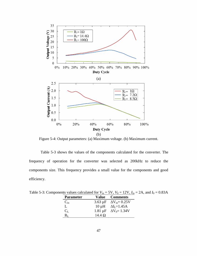
47
(a)
(b)
Figure 5-4: Output parameters: (a) Maximum voltage. (b) Maximum current.
Table 5-3 shows the values of the components calculated for the converter. The
frequency of operation for the converter was selected as 200kHz to reduce the
components size. This frequency provides a small value for the components and good
efficiency.
Table 5-3: Components values calculated for Vin = 5V, V0 = 12V, Iin = 2A, and I0 = 0.83A
Parameter Value Comments
Cin 3.63 µF ΔVin= 0.25V
L 10 µH ΔIL=1.45A
CL 1.81 µF ΔV0= 1.34V
RL 14.4 Ω

48
The converter was simulated, using the parameters in Table 5-3. In the simulation,
a PV sub-panel was used as input source. Power FETs of 8m ON resistance were used.
Losses due to effective series resistance (ESR) from the capacitors and inductor were
included. The test results are shown in Figure 5-5. The figure demonstrates that all the
parameters stay inside the desired specifications. The input voltage waveform shows a
ripple of 25mV with a DC value of 5V. The inductor current is 2A with a ripple of 1.45A
and the output voltage is approximately 12V with a ripple of 1.34V.
Figure 5-5: Transients results of the boost converter using the values in Table 5.3.
5.3 CURRENT SENSOR CIRCUIT
The current-to-digital converter (IDC) sensor was implemented in a 5V, 0.7m, 3
level-metal CMOS technology. The top level diagram of the current sensor is shown in

49
Figure 5-6. This current sensor architecture can be divided in two sections: the front end
(switches, capacitors and current source) and the comparator (pre-amps, latch).
Vcm
2C1C
clk
2
1
21
Cblock
Cblock
Bia
sin
g
Co
ntr
ol
Isink
Counter
E
Enable
Logic
2
M1
M2
Front End
Comparator
K
+
V0
–
Figure 5-6: Top level schematic of the current sensor.
Sensor Specifications
The IDC was implemented to sense the output current of the boost converter
(output parameters of 12V and 832mA). The target specifications are listed in Table 5-4.
The sensor will provide an 8 bits output that represent a sensed current range of 832 mA
with a minimum sensed value of 3.25 mA. The converter is driven by a PWM signal with
frequency fs = 200kHz. The sampling time (tsample) used for the sensor is 10% of the
period (500s). Finally, the minimum detectable voltage change (V) is targeted to be 1
mV.
Table 5-4: Specifications of the Current-to-Digital converter circuit.
Parameter Value
Resolution 8 bits
Full Scale Current 832 mA
LSB 3.25 mA
DNL < 1 LSB
INL < 1 LSB
Clock Frequency (fclk) 10 MHz
Sampling time (tsample) 500 ns
Minimum (V) 1 mV

50
Sensor Front End
The sensor front end is composed by the sample stage and the current source as
shown in Figure 5-6. At the input of the IDC, two DC block capacitors are used. For this
design, the DC block capacitors are external to the IC. External capacitors allow the
selection of devices with dielectric breakdown voltage above the boost output voltage.
The value of these capacitors is considerably larger than the internal sampling caps (Cblock
is much larger than C1 and C2) to decrease the effect of the voltage divider between the
caps.
In the process of sampling, feed-through will occur. The feed-through is the result
of the fast transient in the digital sampling signal. To decrease this effect, CMOS
transmission gates were used. The transmission gates use complementary control signals
that result in a reduction of the feed-through effect. The capacitors are differentially
connected to the comparator. If the sampling switches are matched, the same amount of
additional charges will enter both caps. Therefore, feed-through will be rejected as
common mode noise.
The sampling capacitors and current source (Isink) were selected based in the
equations presented in Chapter 4 and the specifications in Table 5-4. A cascaded current
source was used to reduce the voltage dependence on the current value. The current
source is enabled/disabled by controlling the biasing point of the cascaded transistor. The
selected capacitors and current source values are shown in Table 5-5.
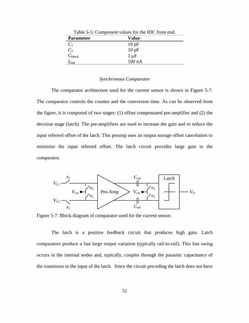
51
Table 5-5: Component values for the IDC front end.
Synchronous Comparator
The comparator architecture used for the current sensor is shown in Figure 5-7.
The comparator controls the counter and the conversion time. As can be observed from
the figure, it is composed of two stages: (1) offset compensated pre-amplifier and (2) the
decision stage (latch). The pre-amplifiers are used to increase the gain and to reduce the
input referred offset of the latch. This preamp uses an output storage offset cancelation to
minimize the input referred offset. The latch circuit provides large gain to the
comparator.
Pre-AmpVcm Vcm
LatchCoff
Coff
x1
x1
x2
x2
x2
x2
VC1
VC2
VO
Figure 5-7: Block diagram of comparator used for the current sensor.
The latch is a positive feedback circuit that produces high gain. Latch
comparators produce a fast large output variation (typically rail-to-rail). This fast swing
occurs in the internal nodes and, typically, couples through the parasitic capacitance of
the transistors to the input of the latch. Since the circuit preceding the latch does not have
Parameter Value
C1 10 pF
C2 10 pF
Cblock 1 F
Isink 100 nA

52
zero output impedance, the signal couples back to its input. This distortion is called
kickback and it affects the accuracy of the comparator.
Figure 5-8 shows the latch circuit used in this design. This circuit contains a pre-
amp, a positive feedback stage and a differential to single ended buffer. Transistors
mismatches are present in the different stages of this latch circuit. These mismatched
results in an offset in the comparator. The offset of the designed latch was simulated
using a Monte Carlo simulation (see Figure 5-9). This simulation indicates that the
designed latch has an offset of VOS-Latch = 64 mV (3 sigma). To decrease the input
referred offset of the comparator a pre-amplifier has to be added.
The pre-amplifier gain is selected to maintain the input referred offset below the
spec of 1mV. The calculation of the input referred offset (VOS) is as follows:
OS-LatchOS OS-Pre-Amp
Pre-Amp
VV V
A (25)
where VOS-Pre-Amp and APre-Amp are the offset voltage and gain of the pre-amplifier,
respectively. The offset of the pre-amplifier is compensated with the offset storage
technique; thus it is neglected for the analysis (VOS-Pre-Amp ≈ 0V). To reduce the latch
offset voltage below 1mV the gain of the pre-amplifier has to be above 64 V/V.

53
Vb
M41M31
M2M1
M5
M4M3
vop vom
vmvp
VDD VDD
M6 M7 M8 M9
Buffvom
vop
vout
Figure 5-8: Latch circuit with pre-amplification [61].
Figure 5-9: Monte Carlo simulation to test the offset of the latch. The 3 sigma offset is 64
mV.
The pre-amplifier design targets a gain above 70V/V. The output offset
cancelation requires a low gain amplifier to avoid saturation on the offset storage cycle (A
< 10 V/V). For the offset cancelation, a 10MHz clock is used, which requires a large
bandwidth amplifier. Figure 5-10 shows the amplifier selected for the pre-amplifier. This
circuit provides a fully differential amplifier with internal common mode feedback and
easy gain control. To achieve the bandwidth, the gain of the pre-amplifier was decreased

54
to 3 V/V as shown in Figure 5-11. Due to the low gain, four pre-amplifiers are cascaded
reaching a gain of approximately 81 V/V. From equation (25), the combined input
referred offset of the comparator (pre-amp + latch) is 0.79 mV.
R R
Vin+Vin–
Vb
M4M3
M2M1
M2
Figure 5-10: Pre-amplifier circuit schematic.
Figure 5-11: Gain and phase of the pre-amplifier.
The input of the pre-amplifier has switches for the output offset storage. In every
offset cancelation cycle, the switches inject charges to the sampling capacitors distorting

55
the stored voltage. To avoid this distortion, an instrumentation amplifier with gain of
3V/V was used to buffer, or isolate, these two nodes (Figure 5-12). This stage
(instrumentation amplifier) will now dominate the comparator offset. The offset of the
instrumentation amplifier depends on the matching of the transistors, current, resistor,
etc. This offset is difficult to be reduced under the desired specs. Figure 5-13 shows the
offset obtained after optimization of the instrumentation amplifier.
VC2
VC1
Vout
+
–
+
–
+
–
R
R
R
RR
R
R
Figure 5-12: Instrumentation amplifier schematic.
Figure 5-13: Monte Carlo simulation to test the instrumentation amplifier’s offset.

56
CHAPTER 6
MEASUREMENTS AND ANALYSIS
A board with the boost DC-DC converter and current sensor IC was implemented
to characterize the performance of the proposed system, as shown in Figure 6-1. A panel
of 15W was used for the test (15V and 1A). The boost converter performs the MPPT at
the sub-panel level (5V). The specifications of the boost converter are listed in Table 6-1.
The current sensor IC is connected to the output of the converter to sense the output
current, as illustrated in Figure 6-1c. The proposed current-to-digital converter was
designed and fabricated on a 5V, 0.7 m, 3 metallization-layer CMOS technology
(Figure 6-1b). The testing was divided in three parts:
1. Current sensor characterization: In this test, the current sensor performance was
tested under a controlled environment (voltage, temperature and boost converter
load were controlled). This allows the correct characterization of the linearity,
offset and other parameters of the IDC.
2. Indoor PV test: This test characterizes the PV system on the lab. Performing the
test in a lab allows controlling the shading and temperature of the panels. The
board was connected to do MPPT to a panel with two sub-panels as well as for the
individual sub-panels.
3. Outdoor PV Test: The system was tested under real environment to verify it can
provide the correct power optimization. In this test, the panel and sub-panel
optimization were examined and compared in real conditions.
The test, results and analysis will be explained in the following sections.

57
DC-DC Converter
+
Vout
–
L+
_
Vin
iL
CL RL
Digital
Controller/
MPPT
Cblock
S1, S2
S1
S2
IDC
digital
output
Current Sensor/
IDC
AD
C
Cin
(a)
InputSample Caps.
Co
mp
arat
or
wit
h
off
set
can
cella
tio
n
Logi
c
(b)
IDC
DC-DC BOOST CONVERTER
(c)
Figure 6-1: Prototype board used to characterize the IDC IC and test MPPT. (a)Block
diagram of the board. (b) Photo of the IDC IC. (c) Photo of the Board.

58
Table 6-1: Specifications of the prototype boost converter.
No. Parameter Value Comments
1 Power Supply (VDD) 5V 2 Input Voltage (Vin) 5V 3 Output Voltage (Vout) 12V 2.4x Boost 4 Frequency ( f ) 200kHz 5 Input Current (Iin) 2A 6 Input Current Ripple (ΔIin) 1 – 4A 7 Output Current (Iout) 0.833A 8 Output Voltage Ripple (ΔVout) 1.34V Based on Current sensor IC
6.1 CURENT SENSOR CHARACTERIZATION
The current sensor characterization uses an input DC source for the boost
converter. The use of a DC source allows a controlled characterization of the current
sensor and the DC-DC converter. The converter circuit was designed to boost 5V to 12V
with a switching frequency of 200 kHz, CL = 1.8 µF and a load of 14.4 Ω. For the IDC, a
clock of 10MHz was used in the comparator and in the 8 bits counter. The values of the
DC block (Cblock) and sensing (C1, C2) capacitors were 1uF and 10pF, respectively. The
sampling time was 500ns from the sampling in C1 to C2. The selected values allows a
least-significant-bit (LSB) resolution of 3.24 mA.
Two DC sources were connected to the input of the current sensor to characterize
the offset of the comparator. The characterization consists in keeping a constant voltage
at the non-inverting input of the comparator and varying the voltage of the inverting input
until the output state changes. This test was repeated for supply voltages of 4.5V to 5.5V,
as shown in Figure 6-2. The offset of the comparator is 3 mV for a power supply voltage
of 5V. This offset can be now compensated later on the digital controller.

59
Figure 6-2: Measurement of the offset of the comparator.
The next step was to test the current sensor, using the boost converter with an
input DC source. In this test, the input of the boost converter is set to 5V and the duty-
cycle is adjusted to get an output voltage of 12V with a load of 14.4iL = 833mA.
Figure 6-3 shows the measured waveforms of the current sensor. Figure 6-3a shows the
voltage ripple at the output of the DC block capacitor (Cblock, 2.5V common mode). This
ripple contains the information of the load current of the DC-DC converter. Figure 6-3b
illustrates the sampling signals 1 and 2. The time difference between these two signals
define the time t = 500ns, where the voltage ripple is sampled. The sampling of the
voltage ripple in the capacitors (C1 and C2) and the discharge time of capacitor C1 are
shown in Figure 6-3c. The comparator changes state to stop the counter 28s after
2(when the voltages at VC1 = VC2), as shown in Figure 6-3d.

60
(a)
(b)
(c)
(d)
Figure 6-3: Transient measurement of the current sensor. (a) Voltage ripple after the DC
block capacitor (2.5V common mode). (b) Sampling signals (1 and 2). (c) Voltage on
the capacitors C1 and C2. (d) Output signal of the comparator.

61
Then, the load current (iL) was varied from 0A to full-scale (FS = 830mA). The
output digital code was recorded to test the linearity of measurements. The measured and
estimated currents versus the digital output code are presented in Figure 6-4. Based on
these results, the differential non-linearity (DNL) of the converter was extracted. Figure
6-5a demonstrates that a DNL of less than half LSB is achieved by the proposed current
to digital converter. The IDC achieves an integral-non-linearity (INL) of less than one
LSB as shown in Figure 6-5b. This result verifies that the converter maintains an accurate
output over the FS.
Figure 6-4: Response of the 8 bits counter output due to variation in current. The figure
compares the measured results and the values estimated using an ideal output.
The small error in the DNL and INL metrics are due to the quantization errors of
the discrete sampling time, the time constant (between the sampling capacitor and the
switch ON resistance), switches charge injection, and other random measurement errors.

62
(a)
(b)
Figure 6-5: Measured IDC performance. (a) DNL. (b) INL
After that, the sensing power consumption of the IDC (capacitor charge transfer)
was compared to the resistor based method (I2R losses), excluding any peripheral (ADC,
amplifiers, etc.), as shown in Figure 6-6. As shown in Figure 6-6, the power consumed by
sensing with the IDC is in the order of the nW, while the resistor sensor consumption is
in mW (around 5 orders of magnitude larger).
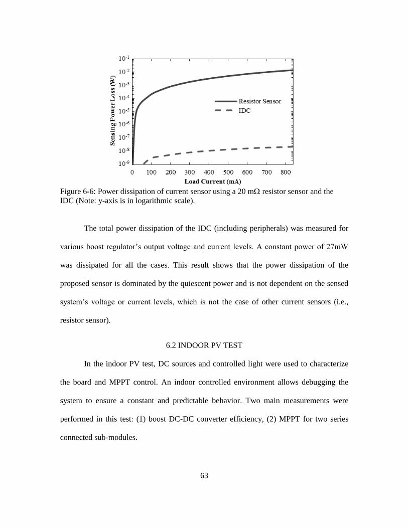
63
Figure 6-6: Power dissipation of current sensor using a 20 m resistor sensor and the
IDC (Note: y-axis is in logarithmic scale).
The total power dissipation of the IDC (including peripherals) was measured for
various boost regulator’s output voltage and current levels. A constant power of 27mW
was dissipated for all the cases. This result shows that the power dissipation of the
proposed sensor is dominated by the quiescent power and is not dependent on the sensed
system’s voltage or current levels, which is not the case of other current sensors (i.e.,
resistor sensor).
6.2 INDOOR PV TEST
In the indoor PV test, DC sources and controlled light were used to characterize
the board and MPPT control. An indoor controlled environment allows debugging the
system to ensure a constant and predictable behavior. Two main measurements were
performed in this test: (1) boost DC-DC converter efficiency, (2) MPPT for two series
connected sub-modules.

64
To test the efficiency of the boost converter, the input was connected to a constant
5V power supply. The load of the converter was varied to sweep the power processed by
device from full load to no-load. Figure 6-7 shows the measured efficiency. The
efficiency stays above 94% for load greater than 5W.
Figure 6-7: Efficiency of the boost DC-DC converter.
The configuration used to test the MPPT control is shown in Figure 6-8. In this
test, the MPPT is performed using the output parameters of the converter, as shown in
Figure 6-8a. The system consists of the PV panel, boost DC-DC converter, voltage and
current sensors, and the digital control. The test setup shown in Figure 6-8b consists in
the artificial light source, dimmer (to simulate shading), solar panel and prototype board.

65
MPPT
Controller
IDC
digital
output
X
+
–
Z-1
+
–A1
3 2 1 0A0
Pulse Generator
and Drivers
-
Z-1
ΔD
+
+–
++
D(n)I0(n)
P0(n)
P0(n-1)
ΔD > 0 ?
ΔP0 > 0 ?
D(n
-1)
D(n-1) - ΔD
D(n-1) + ΔD
DC-DC Converter
+
V0
–
L+
_
Vin
iL
CL RL
Cblock
S1
S2
Current Sensor/
IDC
AD
C
V0(n)
D(n-1)
D(n)
1:Yes
0:No
(a)
(b)
Figure 6-8: Setup used for the indoor MPPT test. (a) Block diagram of the system. (b)
Physical setup.
The processing for this MPPT circuit consists of a perturb-and-observe (P&O)
method, shown in Figure 6-8a [62, 63]. The output parameters V0(n) and I0(n) are
measured and the power P0(n) is calculated. The calculated power and duty cycle are

66
compared with their respective previous states [i.e., P0(n) > P0(n-1) and D(n) > D(n-1)].
Based on the present state, the algorithm decides the new duty-cycle [D(n-1) + D or
D(n-1) – D] to optimize the output power of the system.
The system was tested to ensure it can correctly perform the MPPT. Figure 6-9
displays the results of the output MPPT algorithm using the proposed current sensor. The
I-V curves were taken using a Daystar DS-100C I-V Curve Tracer [64] and the power
operating point of the converter was captured using an oscilloscope (Tektronix
TDS7104). The graph includes the I-V curve of the panel for two incident light intensities
(0% shade and 50% shade). The yellow cloud shows the operating point achieved by the
system. In the two cases, the proposed system tracks correctly the maximum power
points of the PV input.
Figure 6-9: Test of the output MPPT algorithm using the proposed current sensor.
The sub-panel MPPT was tested using two sub-panels. The two configurations
under test are shown in Figure 6-10. Two tests were used to compare the MPPT at both
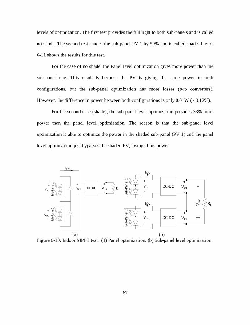
67
levels of optimization. The first test provides the full light to both sub-panels and is called
no-shade. The second test shades the sub-panel PV 1 by 50% and is called shade. Figure
6-11 shows the results for this test.
For the case of no shade, the Panel level optimization gives more power than the
sub-panel one. This result is because the PV is giving the same power to both
configurations, but the sub-panel optimization has more losses (two converters).
However, the difference in power between both configurations is only 0.01W (~ 0.12%).
For the second case (shade), the sub-panel level optimization provides 38% more
power than the panel level optimization. The reason is that the sub-panel level
optimization is able to optimize the power in the shaded sub-panel (PV 1) and the panel
level optimization just bypasses the shaded PV, losing all its power.
DC-DC+
Vout
-
+ Vin2
-
+ Vin3
-
Ipv
RL...
Sub
-Pan
el 1
...
Sub
-Pan
el 2
+ Vin1
-
DC-DC+
VO1
-
+ Vin
-
Ipv
DC-DC+
VO2
-
+ Vin
-
Ipv|
V
ou
t
+
RL
...
Sub
-Pan
el 2
...
Sub
-Pan
el 1
(a) (b)
Figure 6-10: Indoor MPPT test. (1) Panel optimization. (b) Sub-panel level optimization.
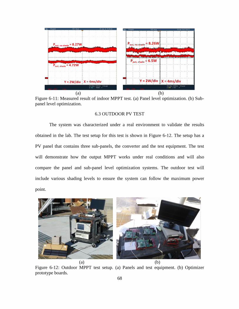
68
(a) (b)
Figure 6-11: Measured result of indoor MPPT test. (a) Panel level optimization. (b) Sub-
panel level optimization.
6.3 OUTDOOR PV TEST
The system was characterized under a real environment to validate the results
obtained in the lab. The test setup for this test is shown in Figure 6-12. The setup has a
PV panel that contains three sub-panels, the converter and the test equipment. The test
will demonstrate how the output MPPT works under real conditions and will also
compare the panel and sub-panel level optimization systems. The outdoor test will
include various shading levels to ensure the system can follow the maximum power
point.
(a) (b)
Figure 6-12: Outdoor MPPT test setup. (a) Panels and test equipment. (b) Optimizer
prototype boards.

69
The prototype board was used to test the MPPT control with the proposed current
sensor. Four shading patterns were used for this test (0%, 13%, 40% and 50% shade).
Figure 6-13 shows the I-V curves and the measured output power for each shading
condition. The results show that the proposed system accurately follows the maximum
power point under various shading conditions.
(a)
(b)
Figure 6-13: Prototype measurements using output MPPT employing the IDC sensor over
five shading cases. (a) I-V curve. (b) Power vs. voltage curve.

70
A panel with three sub-panels was used to test and compare the performance of
the proposed system outdoor. The two setups used in this test were the panel level
optimization and the proposed sub-panel level optimization (similar to the indoor setup),
as shown in Figure 6-14. The panel level uses a single converter to optimize the power of
the entire panel. The sub-panel level system removes the bypass diodes and optimizes the
power of each sub-panel circuit.
DC-DC+
Vout
-
+ Vin3
-
+ Vin 2
-
+ Vin1
-
+ Vin4
-
Ipv
RL
...
Sub
-Pan
el 3
...
Sub
-Pan
el 1
...
Sub
-Pan
el 2
DC-DC+ V3
-
+ Vin3
-
Ipv
DC-DC+ V2
-
+ Vin2
-
Ipv
DC-DC+ V1
-
+ Vin1
-
Ipv
|
Vo
ut
+
RL
...
Sub
-Pan
el 3
...
Sub
-Pan
el 2
...
Sub
-Pan
el 1
(a) (b)
Figure 6-14: Outdoor MPPT test setup. (a) Panel level MPPT. (b) Sub-panel level MPPT.
Five shading patterns were used to test the two PV optimization systems, as
shown in Figure 6-15. The maximum output power was recorded for both systems under
each case. The cases under study were the following:
1. No-shade: This means that the three sub-panels were unshaded.
2. Sub-Panel 1 (25% Shade): This test shades only sub-panel 1 by 25%. Sub-panels
2 and 3 are unshaded.

71
3. Sub-Panel 2 (65% Shade): This test shades only sub-panel 2 by 65%. Sub-panels
1 and 3 are unshaded.
4. Sub-Panel 3 (50% Shade): This test shades only sub-panel 3 by 50%. Sub-panels
1 and 2 are unshaded.
5. Sub-Panel 1 (25%) & Sub-Panel 3 (50%) Shade: This test shades sub-panel 1 by
25%, sub-panel 3 by 50%. Sub-panel 2 unshaded.
Figure 6-15: I-V curve of the three sub-panels. The graphs show the I-V curves of the
three sub-panels under no shade and shade conditions.

72
The results for the five shading patterns were recorded for both optimization
systems. Figure 6-16 shows the results of the panel level optimization. When shading is
applied to the panel level system, the shaded sub-panel limits the performance of the
unshaded sub-panels. If the shading is high enough the bypass diodes short the shaded
sub-panels. This causes the power of the shaded sub-panel to be lost.
(a)
(b)
Figure 6-16: Results of the panel level optimization for all the shading patterns. (a) IV
curve. (b) Power vs. voltage curve.
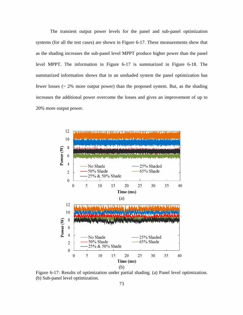
73
The transient output power levels for the panel and sub-panel optimization
systems (for all the test cases) are shown in Figure 6-17. These measurements show that
as the shading increases the sub-panel level MPPT produce higher power than the panel
level MPPT. The information in Figure 6-17 is summarized in Figure 6-18. The
summarized information shows that in an unshaded system the panel optimization has
fewer losses (~ 2% more output power) than the proposed system. But, as the shading
increases the additional power overcome the losses and gives an improvement of up to
20% more output power.
(a)
(b)
Figure 6-17: Results of optimization under partial shading. (a) Panel level optimization.
(b) Sub-panel level optimization.

74
(a)
(b)
Figure 6-18: Output power for the panel and sub-panel optimization systems for different
shading patterns. (a) Comparison of output power. (b) Power as shading increase in a
single sub-panel and percentage of improvement of sub-panel vs. panel MPPT.

75
CHAPTER 7
CONCLUSIONS AND RECOMENDATIONS
This dissertation introduces an improved MPPT system and a low loss standard
CMOS current sensor. The system was tested in a low power PV panel, which can easily
be scaled to high power applications. In this chapter, the conclusion and the
recommendations for future improvements of the system and tests will be discussed.
7.1.CONCLUSIONS
A sub-panel level optimization system and a current to digital converter were
presented. These two combined systems represent a step toward the integration of the
power optimizer for PV systems to a single IC. The sub-panel level optimization reduces
the power levels per converter and the current sensor was integrated and tested for this
application.
The proposed current-to-digital sensor uses standard CMOS, dissipates low power
and allows high common mode range sensing. This fully integrated circuit uses a charge
based current sensing method that allows high voltage sensing with standard CMOS
process. The sensor produces accurate sensing output, has high efficiency and requires a
small number of components and area. The IDC gives a direct digital output and can be
integrated to a digitally controlled system without the need of complex ADC. The sensor
is a standard CMOS circuit that can be used for DC-DC converters and other high-
voltage applications including DC motor control, buck/boost converters, regulators,
rectifiers, and inverters without the need for high-voltage process. Measurements for a
current range from 0 to 830mA showed accuracy of 99.6% with DNL of less than half

76
LSB, INL of less than one LSB and total power consumption of 27mW. The sensor was
successfully integrated to a PV system for MPPT.
The sub-panel level optimization together with the proposed current sensor
improves the optimization under partial shading by up to 20%. The sub-panels produce
lower power compared to the panel. This power reduction allows relaxing the power
stress of the system components. The boosting of the output voltage allows the reduction
of the output current and parallel connection of the panels. The sub-panel level MPPT
follows closely the maximum available power with a converter efficiency of around 90%
to 95%.
The use of this architecture enables: (1) use of relaxed specifications for the
individual converters (eliminate transformers and electrolytic capacitors.), (2) reduction
in voltage/power stress for components, (3) improve the power generated under partial
shading and other mismatches, (4) allows the parallel connection of panels for simpler
and modular system expansion, (5) improve the reliability of each converter, and (6)
improve the availability of the system (if one converter fails, only 1/3 of the panel’s
power is lost).
The converter and current sensor presented in this research provide a first step
toward the integration of the PV system. They accurately sense and follow the MPPT of
the panels and reduce the power handling to facilitate this integration.
7.2. RECOMENDATIONS
This research proposed a sub-panel level MPPT system which reduces the
complexity and power stress on each converter. The used prototype proves the concept

77
with a low power panel. A current sensor was also introduced and tested to verify its
performance. To improve the system and the testing, few more steps are recommended:
1. Build the complete system with the boost double lift converter and the partial
power processing converter in a single board. This will allow having the correct
conversion ratio and regulated output.
2. This new system will allow a comprehensive cost and efficiency analysis.
3. Design and test the sub-panel MPPT converter for the typical residential panels
(180 W).
4. Second step of integration of the sub-panel system. Integration of the drivers,
control, sensors and peripherals in the same IC. This will result in a significant
reduction of the sizes and price of each converter.
These steps will allow the optimization of the system to reduce its area and costs.
The reduction in costs and size will make this system economically affordable for future
commercialization.
78
REFERENCES
[1] S. P. Poshtkouhi, V.; Fard, M.; Trescases, O., "A General Approach for
Quantifying the Benefit of Distributed Power Electronics for Fine Grained MPPT
in Photovoltaic Applications Using 3-D Modeling," IEEE Trans. Power Electron.,
vol. 27, pp. 4656-4666, Nov. 2012 2012.
[2] S. Poshtkouhi, A. Biswas, and O. Trescases, "DC-DC converter for high
granularity, sub-string MPPT in photovoltaic applications using a virtual-parallel
connection," in 2012 27th Annu. IEEE Applied Power Electronics Conf. and
Expo. (APEC), 2012, pp. 86-92.
[3] R. A. Messenger and J. Ventre, Photovoltaic System Engineering, 2nd ed.: CRC
Press LLC, 2004.
[4] OvieraSolar, "Mono-Crystalline Solar Module - 72 Cells," in OS180M datasheet,
ed, April 2011 [Revise June. 2014].
[5] Suniva, Suniva optimus series monocrystalline solar modules. Suniva, April 14,
2014 (Revised June, 2014).
[6] J. K. Mathew, J. Kuitche, and G. TamizhMani, "Test-to-failure of PV modules:
Hotspot testing," in 2010 35th IEEE Photovoltaic Specialists Conf. (PVSC), 2010,
pp. 002839-002843.
[7] Z. Qi and L. Qun, "Temperature and reverse voltage across a partially shaded Si
PV cell under hot spot test condition," in 2012 38th IEEE Photovoltaic Specialists
Conf. (PVSC), 2012, pp. 001344-001347.
[8] T. Esram and P. L. Chapman, "Comparison of Photovoltaic Array Maximum
Power Point Tracking Techniques," IEEE Trans. Energy Convers., vol. 22, pp.
439-449, 2007.
[9] N. Mutoh, M. Ohno, and T. Inoue, "A Method for MPPT Control While
Searching for Parameters Corresponding to Weather Conditions for PV
Generation Systems," IEEE Trans. Ind. Electron., vol. 53, pp. 1055-1065, 2006.
79
[10] D. Sera, L. Mathe, T. Kerekes, S. V. Spataru, and R. Teodorescu, "On the
Perturb-and-Observe and Incremental Conductance MPPT Methods for PV
Systems," IEEE Journal of Photovoltaics, vol. 3, pp. 1070-1078, 2013.
[11] Y. Moghe, T. Lehmann, and T. Piessens, "Nanosecond Delay Floating High
Voltage Level Shifters in a 0.35 m HV-CMOS Technology," IEEE J. Solid-State
Circuits, vol. 46, pp. 485-497, 2011.
[12] X. Ouyang, "Desing and characterization results of integrating CMOS-compatible
high-voltage MOSFETs in a 0.5 m CMOS process," Master of Science,
Electrical Engineering, Washington State University, Washington State
University, 1998.
[13] C. Deline, B. Marion, J. Granata, and S. Gonzalez. (January 2011). A
Performance and Economic Analysis of Distributed Power Electronics in
Photovoltaic Systems, [National Renewable Energy Laboratory, Technical
Report]. Available: www.nrel.gov/docs/fy11osti/50003.pdf
[14] P. Tsao, S. Sarhan, and I. Jorio, "Distributed max power point tracking for
photovoltaic arrays," in 2009 34th IEEE Photovoltaic Specialists Conf. (PVSC),
2009, pp. 002293-002298.
[15] H. Patel and V. Agarwal, "MATLAB-Based Modeling to Study the Effects of
Partial Shading on PV Array Characteristics," IEEE Trans. Energy Convers., vol.
23, pp. 302-310, 2008.
[16] K. Takigawa, N. Okada, N. Kuwabara, and M. Yamaguchi, "A development of
smart power conditioner for value added PV application," in 2000 Conf. Rec. of
the 28th IEEE Photovoltaic Specialists Conf., 2000, pp. 1652-1655.
[17] M. S. Agamy, M. Harfman-Todorovic, A. Elasser, J. A. Sabate, R. L.
Steigerwald, J. Yan, et al., "Dc-dc converter topology assessment for large scale
distributed photovoltaic plant architectures," in 2011 IEEE Energy Conv. Congr.
and Expo. (ECCE), 2011, pp. 764-769.
[18] S. B. Kjaer, J. K. Pedersen, and F. Blaabjerg, "A review of single-phase grid-
connected inverters for photovoltaic modules," IEEE Trans. Ind. Appl., vol. 41,
pp. 1292-1306, 2005.
80
[19] V. Pandya and A. K. Agarwala, "Efficient PV micro-inverter with isolated
output," in 2012 IEEE 5th Power India Conf., 2012, pp. 1-5.
[20] N. Pragallapati and V. Agarwal, "Flyback configuration based micro-inverter with
distributed MPPT of partially shaded PV module and energy recovery scheme," in
2013 IEEE 39th Photovoltaic Specialists Conf. (PVSC), 2013, pp. 2927-2931.
[21] L. Bangyin, L. Chaohui, and D. Shanxu, "Design considerations and topology
selection for dc-module-based building integrated photovoltaic system," in ICIEA
2008. 3rd IEEE Conf. on Industrial Electronics and Applications, 2008., 2008,
pp. 1066-1070.
[22] S. Poshtkouhi, J. Varley, R. Popuri, and O. Trescases, "Analysis of distributed
peak power tracking in photovoltaic systems," in 2010 International Power
Electronics Conf. (IPEC), 2010, pp. 942-947.
[23] X. Weidong, N. Ozog, and W. G. Dunford, "Topology Study of Photovoltaic
Interface for Maximum Power Point Tracking," IEEE Trans. Ind. Electron., vol.
54, pp. 1696-1704, 2007.
[24] W. Feng, W. Xinke, F. C. Lee, W. Zijian, K. Pengju, and Z. Fang, "Analysis of
Unified Output MPPT Control in Subpanel PV Converter System," IEEE Trans.
Power Electron., vol. 29, pp. 1275-1284, 2014.
[25] W. Feng, W. Xinke, F. C. Lee, and Z. Fang, "Analysis of unified output MPPT
control in Sub-Panel PV converter system," in 2013 15th European Conf. on
Power Electronics and Applications (EPE), 2013, pp. 1-8.
[26] J. Stauth, M. Seeman, and K. Kesarwani, "A high-voltage CMOS IC and
embedded system for distributed photovoltaic energy optimization with over 99%
effective conversion efficiency and insertion loss below 0.1%," in 2012 IEEE Int.
Solid-State Circuits Conf. Dig. of Tech. Papers (ISSCC), 2012, pp. 100-102.
[27] J. T. Stauth, M. D. Seeman, and K. Kesarwani, "Resonant Switched-Capacitor
Converters for Sub-module Distributed Photovoltaic Power Management," IEEE
Trans. Power Electron., vol. 28, pp. 1189-1198, 2013.

81
[28] J. T. Stauth, M. D. Seeman, and K. Kesarwani, "A Resonant Switched-Capacitor
IC and Embedded System for Sub-Module Photovoltaic Power Management,"
IEEE J. Solid-State Circuits, vol. 47, pp. 3043-3054, 2012.
[29] S. V. Dhople, A. Davoudi, Domi, x, G. nguez, x, et al., "A Unified Approach to
Reliability Assessment of Multiphase DC-DC Converters in Photovoltaic Energy
Conversion Systems," IEEE Trans. Power Electron., vol. 27, pp. 739-751, 2012.
[30] G. Petrone, G. Spagnuolo, R. Teodorescu, M. Veerachary, and M. Vitelli,
"Reliability Issues in Photovoltaic Power Processing Systems," IEEE Trans. Ind.
Electron., vol. 55, pp. 2569-2580, 2008.
[31] J. H. Wohlgemuth and S. R. Kurtz, "How can we make PV modules safer?," in
2012 38th IEEE Photovoltaic Specialists Conf. (PVSC), 2012, pp. 003162-
003165.
[32] M. Alahmad, M. A. Chaaban, and L. Siu-Kit, "An Adaptive photovoltaic-inverter
topology," in 2011 IEEE PES Innovative Smart Grid Technologies (ISGT), 2011,
pp. 1-7.
[33] J. P. Storey, P. R. Wilson, and D. Bagnall, "Improved Optimization Strategy for
Irradiance Equalization in Dynamic Photovoltaic Arrays," IEEE Trans. Power
Electron., vol. 28, pp. 2946-2956, 2013.
[34] Z. Ye, Y. Ling, and B. Lehman, "Reconfigurable solar photovoltaic battery
charger using a switch matrix," in 2012 IEEE 34th Int. Telecommunications
Energy Conf. (INTELEC), 2012, pp. 1-7.
[35] B. Patnaik, P. Sharma, E. Trimurthulu, S. P. Duttagupta, and V. Agarwal,
"Reconfiguration strategy for optimization of solar photovoltaic array under non-
uniform illumination conditions," in 2011 37th IEEE Photovoltaic Specialists
Conf. (PVSC), 2011, pp. 001859-001864.
[36] J. Storey, P. R. Wilson, and D. Bagnall, "The Optimized-String Dynamic
Photovoltaic Array," IEEE Trans. Power Electron., vol. 29, pp. 1768-1776, 2014.
[37] SolarEdge. (July, 2014). SolarEdge Power Optimizers [Solar Edge, 2014].
Available: http://www.solaredge.us/groups/us/powerbox-power-optimizer
82
[38] TigoEnergy. (July, 2014). Tigo Energy Smart Junction Box [Tigo Energy, 2014].
Available: www.tigoenergy.com/
[39] SolarEdge. (June, 2014). A Comparison of Microinverters & Power Optimizers
[Solar Edge, 2014]. Available:
http://www.solaredge.us/groups/us/technology/microinverters
[40] L. Jiang, "Resistance Control MPPT for Smart Converter PV System," M.S.
Thesis, Electrical Engineering Dept., Virginia Polytechnic Institute. Blacksburg,
Virginia, 2012.
[41] D. T. Thayalan, L. Hwa-Seok, and P. Joung-Hu, "Low-Cost High-Efficiency
Discrete Current Sensing Method Using Bypass Switch for PV Systems," IEEE
Trans. Instrum. Meas., vol. 63, pp. 769-780, 2014.
[42] Q. Tao, X. Lei, and S. Jian, "Dual-Boost Single-Phase PFC Input Current Control
Based on Output Current Sensing," IEEE Trans. Power Electron., vol. 24, pp.
2523-2530, 2009.
[43] L. Ruqi, T. O'Brien, J. Lee, J. Beecroft, and K. Hwang, "A comparative study of
small-signal average models for average current mode control," in 2012 7th Int.
Power Electronics and Motion Control Conf. (IPEMC), 2012, pp. 1729-1736.
[44] C. Huang-Jen, L. Yu-Kang, C. Jun-Ting, C. Shih-Jen, L. Chung-Yi, and M.
Shann-Chyi, "A High-Efficiency Dimmable LED Driver for Low-Power Lighting
Applications," IEEE Trans. Ind. Electron., vol. 57, pp. 735-743, 2010.
[45] M. Rodriguez, V. M. Lopez, F. J. Azcondo, J. Sebastian, and D. Maksimovic,
"Average Inductor Current Sensor for Digitally Controlled Switched-Mode Power
Supplies," IEEE Trans. Power Electron., vol. 27, pp. 3795-3806, 2012.
[46] C. Restrepo, J. Calvente, A. Romero, E. Vidal-Idiarte, and R. Giral, "Current-
Mode Control of a Coupled-Inductor Buck-Boost DC-DC Switching Converter,"
IEEE Trans. Power Electron., vol. 27, pp. 2536-2549, 2012.
[47] C. Restrepo, T. Konjedic, J. Calvente, M. Milanovic, and R. Giral, "Fast
Transitions Between Current Control Loops of the Coupled-Inductor Buck-Boost
DC-DC Switching Converter," IEEE Trans. Power Electron., vol. 28, pp. 3648-
3652, 2013.

83
[48] S. Ziegler, R. C. Woodward, H. H. C. Iu, and L. J. Borle, "Current Sensing
Techniques: A Review," IEEE Sensors J., vol. 9, pp. 354-376, 2009.
[49] L. Chi Yat, P. K. T. Mok, L. Ka Nang, and M. Chan, "An integrated CMOS
current-sensing circuit for low-Voltage current-mode buck regulator," IEEE
Trans. Circuits Syst. II, Exp. Briefs, vol. 52, pp. 394-397, 2005.
[50] L. Cheung Fai and P. K. T. Mok, "A monolithic current-mode CMOS DC-DC
converter with on-chip current-sensing technique," IEEE J. Solid-State Circuits,
vol. 39, pp. 3-14, 2004.
[51] C. Hsiao-Hsing, H. Yuh-Shyan, and C. Jiann-Jong, "An Adaptive Output Current
Estimation Circuit for a Primary-Side Controlled LED Driver," IEEE Trans.
Power Electron., vol. 28, pp. 4811-4819, 2013.
[52] B. Mammano. Jan, 2014). Current Sensing Solutions for Power Supply Designers.
Application Note, Texas Instruments. Available:
http://www.ti.com/lit/ml/slup114/slup114.pdf
[53] F. L. Luo and H. Ye, "Positive output cascade boost converters," IEE Proc. -
Electric Power Applications, vol. 151, pp. 590- 606, 9 Sept. 2004 2004.
[54] E. Marti-Arbona, B. Bakkaloglu, and S. Kiaei, "Ultra-Low Power Current-to-
Digital Sensor for Switching DC-DC Converters," in 2012 8th Conf. on Ph.D.
Research in Microelectronics and Electronics (PRIME), 2012, pp. 1-4.
[55] N. Mohan, T. M. Undeland, and W. P. Robbins, Power Electronics: Converters,
Applications, and Design, 3rd Edition ed.: John Wiley & Sons, 2003.
[56] J. G. Ryan, K. J. Carroll, and B. D. Pless, "A four chip implantable
defibrillator/pacemaker chipset," in 1989 Proc. of the IEEE Custom Integrated
Circuits Conf., 1989, pp. 7.6/1-7.6/4.
[57] L. S. Y. Wong, S. Hossain, A. Ta, L. Weaver, G. Shaquer, A. Walker, et al., "A
very low power CMOS mixed-signal IC for implantable pacemaker applications,"
in 2004 IEEE Int. Solid-State Circuits Conf. Dig. of Tech. Papers (ISSCC), 2004,
pp. 318-530 Vol.1.

84
[58] L. S. Y. Wong, S. Hossain, A. Ta, J. Edvinsson, D. H. Rivas, and H. Naas, "A
very low-power CMOS mixed-signal IC for implantable pacemaker applications,"
IEEE J. Solid-State Circuits vol. 39, pp. 2446-2456, 2004.
[59] Y. K. Ramadass and A. P. Chandrakasan, "Minimum Energy Tracking Loop with
Embedded DC-DC Converter Delivering Voltages down to 250mV in 65nm
CMOS," in 2007 IEEE Int. Solid-State Circuits Conf. Dig. of Tech. Papers (
ISSCC) 2007, pp. 64-587.
[60] M. Wens and M. Steyaert, Design and Implementation of Fully-Integrated
Inductive DC-DC Converters in Standard CMOS. Springer: Springer, 2011.
[61] R. J. Baker, CMOS Circuit design, layout and simulation, Revised 2nd ed.:
Wiley-IEEE Press, 2008.
[62] J. Yuncong, J. A. A. Qahouq, A. Hassan, E. Abdelkarem, and M. Orabi, "Load
current based analog MPPT controller for PV solar systems," in 2012 27th Annu.
IEEE Applied Power Electronics Conf. and Expo. (APEC), 2012, pp. 911-914.
[63] M. Hassani, S. Mekhilef, A. P. Hu, and N. R. Watson, "A novel MPPT algorithm
for load protection based on output sensing control," in 2011 IEEE 9th Int. Conf.
on Power Electronics and Drive Systems (PEDS), 2011, pp. 1120-1124.
[64] Daystar. (2014, June, 2014). DS-100C [Daystar, 2014]. Available:
http://www.daystarpv.com/DS100C.pdf