integrated circuit layout and simulation · 3/7/2012 · learning outcomes by the end of this...
TRANSCRIPT
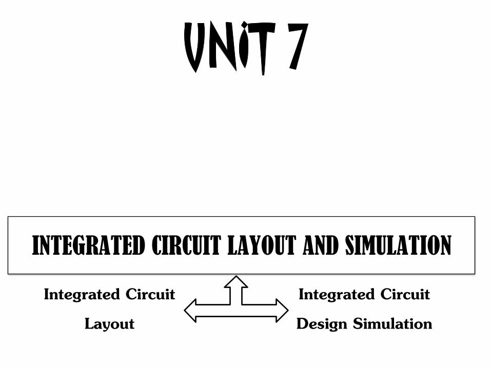
INTEGRATED CIRCUIT LAYOUT AND SIMULATION
Integrated Circuit
Layout
Integrated Circuit
Design Simulation

LEARNING OUTCOMES
By the end of this lecture, student should be able to:
• Define IC layout.
• State the function of IC layouts.
• Transform static CMOS logic circuits (INVERTER, NAND and NOR gate) into stick diagrams using colour codes.
• Describe the connection between actual layouts and stick diagram.
• State the purpose of design rules.
• List 4 general design rules.
• State two measurement units used in geometry rules.
• Describe the geometry rules for width, spacing and projection width and their rationale.

LEARNING OUTCOMES
By the end of this lecture, student should be able to:
• Define simulation in integrated circuit layout.
• Explain the 4 levels of simulation.
• Name a few computer sofware used in simulating circuits in the transistor-level and gate-level.

INTEGRATED CIRCUIT LAYOUT
Definition:
Integrated circuit layout, also known IC layout,IC mask layout, or mask design, is therepresentation of an integrated circuit in termsof planar geometric shapes which correspond tothe patterns of metal, oxide, or semiconductorlayers that make up the components of theintegrated circuit.


INTEGRATED CIRCUIT LAYOUT
Definition:
IC layout is a drawing shapes showing metal tracking, location of n diffusion, p diffusion and polysilicon on the wafer.
Function:
determine the number, connection and floorplan of layers on the wafer according to theprescribed rules.

INTEGRATED CIRCUIT LAYOUT


?
Schematic logic circuit diagramLayout

STICK DIAGRAM
Schematic logiccircuit diagram Layout
Stick diagram
stick diagram is a simple diagram and is a means of capturing topography and layer information.Stick diagrams convey layer information through colour codes or monochrome encoding.

STICK DIAGRAM
Schematic logiccircuit diagram
LayoutStick diagram

STICK DIAGRAM
Schematic logiccircuit diagram
LayoutStick diagram

STICK DIAGRAM
Schematic logiccircuit diagram
Stick diagram

STICK DIAGRAM
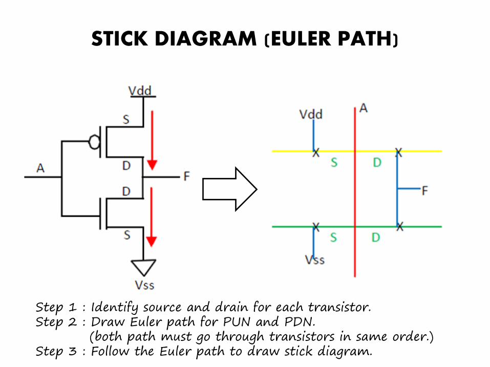
STICK DIAGRAM (EULER PATH)
Step 1 : Identify source and drain for each transistor.Step 2 : Draw Euler path for PUN and PDN.
(both path must go through transistors in same order.)Step 3 : Follow the Euler path to draw stick diagram.

STICK DIAGRAM (EULER PATH)
Step 1 : Identify source and drain for each transistor.Step 2 : Draw Euler path for PUN and PDN.
(both path must go through transistors in same order.)Step 3 : Follow the Euler path to draw stick diagram.

STICK DIAGRAM (EULER PATH)
Step 1 : Identify source and drain for each transistor.Step 2 : Draw Euler path for PUN and PDN.
(both path must go through transistors in same order.)Step 3 : Follow the Euler path to draw stick diagram.

STICK DIAGRAM (EULER PATH)
Step 1 : Identify source and drain for each transistor.Step 2 : Draw Euler path for PUN and PDN.
(both path must go through transistors in same order.)Step 3 : Follow the Euler path to draw stick diagram.
?

Draw the stick diagram for the following schematic CMOS logic circuit.

Draw the stick diagram for the following schematic CMOS logic circuit.

Draw the stick diagram for the following schematic CMOS logic circuit.

DESIGN RULES
Layout
Stick diagram
• Allow translation of circuits (usually in stick diagram or symbolic form) into actual geometry in silicon.
• Interface between circuit designer and fabrication engineer.

Stick diagram

LAYER L-EDIT
p-substrate background
n-well N Well
p+ Active + P Select
n+ Active + N Select
gate Poly
Metal Metal1
connection L-EDIT
Active with Metal Active Contact
Poly with Metal Poly Contact
VDD
VSS
Poly
N Select
P Select
N Well
Active
P Select
N Select
FA
ActiveContact
PolyContact

VDD
VSS
Poly
N Select
P Select
N Well
Active
N Select
P Select
FA
ActiveContact
PolyContact

Is these layout producethe same gate?
Layout 1 Layout 2
VDD
VSS
A F

Is these layout producethe same gate?
Layout 1 Layout 2
VDD
VSS
A F

Is these layout producethe same gate?
Layout 1 Layout 2
VDD
VSS
A F

DESIGN RULES
Layout for NANDStick diagram for NAND
?

DESIGN RULES
Layout for NANDStick diagram for NAND

DESIGN RULES
Layout for NORStick diagram for NOR
?

DESIGN RULES
Layout for NORStick diagram for NOR

CROSS SECTION OF INVERTER

CROSS SECTION OF INVERTER
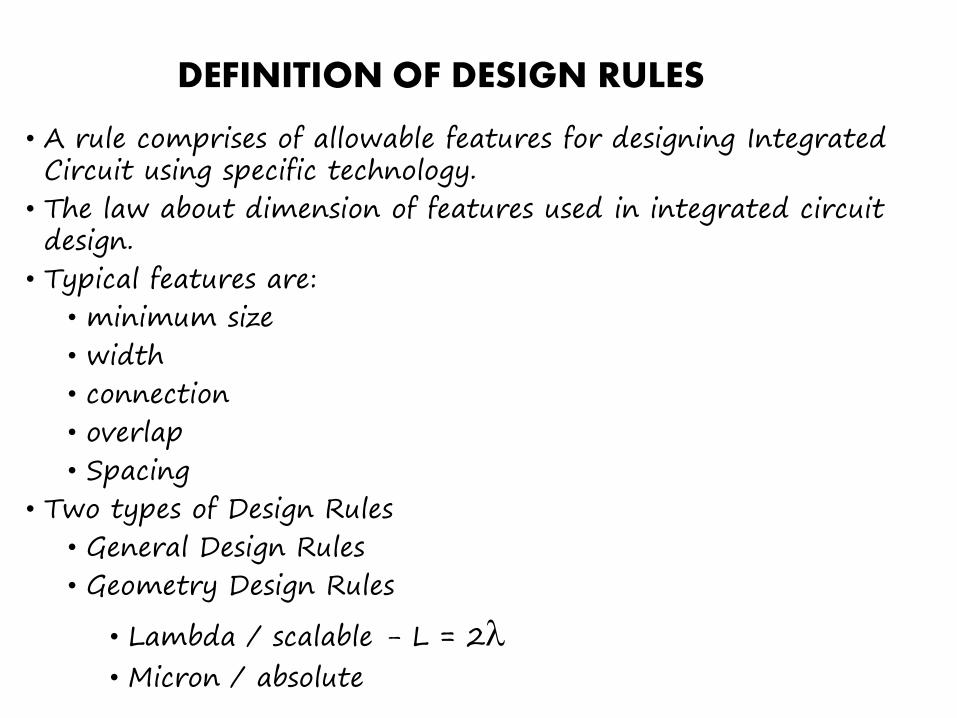
DEFINITION OF DESIGN RULES
• A rule comprises of allowable features for designing Integrated Circuit using specific technology.
• The law about dimension of features used in integrated circuit design.
• Typical features are:• minimum size• width• connection• overlap• Spacing
• Two types of Design Rules• General Design Rules• Geometry Design Rules
• Lambda / scalable - L = 2• Micron / absolute

TYPES OF DESIGN RULES
1. General Design RulesMain objective is to build reliably functional circuits in as small an area as possibleFour General Design Rules:i. Layout must be drawn in the smallest size
possible.ii. Avoid junctions in wide area to prevent current
lost.iii. Minimum number of cross path.iv. Contact must be at side of layout to prevent
cross between layer.

TYPES OF DESIGN RULES
2. Geometry Design Rulesi. lambda based rules / scalable design rules
- known as scalable rules as they allow first order scaling. - Moving from one process to another requires only a change in .
i. micron based rules / absolute design rules- all sizes and spacing specified in microns.
- Rules don’t have to be multiples of . - Can result in 50% reduction in area over based rules. - Standard in industry.


TYPES OF DESIGN RULES
Lambda based rules

Draw these layout at whiteboard…


TYPES OF DESIGN RULES
Lambda based rules- Wires

TYPES OF DESIGN RULES
Lambda based rules- Select

TYPES OF DESIGN RULES
Lambda based rules- Transistor
Wellgate
Active

TYPES OF DESIGN RULES
Lambda based rules- active contact

SIMULATION

SIMULATION

SIMULATION
Definition: the act of imitating the behavior of some situation or some system or environment in order to predict actual behavior.
6 level of simulation:i. Behavioral simulationii. Gate-level simulationiii. Switch-level simulationiv. Transistor-level or
circuit level simulation
http://iroi.seu.edu.cn/books/asics/Book/CH13/CH13.1.htm#pgfId=119950
High level simulation(more abstract)
toLow level simulation
(more detailed)
more accurate,more complex,
longer time to run

BEHAVIORAL SIMULATION
One method models large pieces of a system as black boxes with inputs and outputs.
employs a high level of abstraction to model the design.
allows you to verify syntax and functionality without timing information
Example : four-bit addition operator
Software : VHDL or Verilog

GATE SIMULATION
Penyelakuan aras get akan menerima dan mengeluarkan hanyalogik 1 atau logik 0. Masukan dan keluaran ini akan disemakdengan persamaan logik untuk memastikan ketepatanrekabentuk. Software : PSPICE, PROTEL, S-EDIT

SWITCH SIMULATION
Penyelakuan ini menggunakan transistor sebagai suis/get logikmenjadi satu rangkaian suis transistor. Hasil yang diperolehi diaras ini adalah sama dengan aras get. Software : PSPICE, PROTEL, S-EDIT

TRANSISTOR SIMULATION
more accuracy than provided by switch-level simulation.solve circuit equations exactly, given models for the nonlinear transistors, and predict the analog behavior of the node voltages and currents in continuous time.Costly in computer time.Software : PSICE, S-EDIT, PROTEL

OTHER WAYS…

OTHER WAYS…