int. j. engg. res. & sci. & tech. 2016 m poongodi and … · the sar is analog to digital...
TRANSCRIPT


95
This article can be downloaded from http://www.ijerst.com/currentissue.php
Int. J. Engg. Res. & Sci. & Tech. 2016 M Poongodi and P Jayabalasubramaniyam, 2016
MINIMIZATION OF POWER AND AREA BY USINGDUAL EDGE LATCH FOR SAR AND COMPARATOR
M Poongodi1 and P Jayabalasubramaniam2
The main aim is to reduce area and power by replacing pulsed latches with dual edge latch. Theaverage power, static power and dynamic power are reduced by dual edge latch. Dual edgelatch is combined with inverter coupling circuit. It has MN1 and MN2 as2 NMOS transistor fordual edge latch. The circuit having input as D, Db and output as Q, Qb. When clock is “set”MN1, MN2 both turns “ON”, If clock is “RESET” MN1, MN2 turns “OFF”. This dual edge latchconsumes less static current and power delay product than shift register with pulsed latches. Itcan be used to design Successive Approximation Ratio (SAR) and Comparator. Power alsoreduced and also it uses less amount of transistor than shift register with pulsed latches. Itconsumes 67% power and 46% area when compared to shift register with pulsed latches.
Keywords: Power Delay Product, Tanner, Processor, ASIC
*Corresponding Author: M Poongodi [email protected]
1 PG Scholor (VLSI Design), Sree Sakthi Engineering College, Coimbatore.2 Assistant Professor, Sree Sakthi Engineering College, Coimbatore.
Int. J. Engg. Res. & Sci. & Tech. 2016
ISSN 2319-5991 www.ijerst.comVol. 5, No. 1, February 2016
© 2016 IJERST. All Rights Reserved
Research Paper
INTRODUCTIONThe area and power is very less when compared
to shift register with pulsed latches. The dual
edge latch will be used for reducing average
power, dynamic power and static power. The shift
register with pulsed latches can be used in existing
system in Figure 1. Dual edge latch can be
replaced by pulsed latches and it is used in shift
register applications such as comparator,
successive approximation ratio, etc. The SAR is
analog to digital converter circuit consists of
sample and hold circuit , an analog voltage
comparator an internal reference DAC. Dual edge
latch comprised of two numbers of NMOS
transistors. The inputs are D, Db and outputs
are Q, Qb. When clock is in “SET” condition both
NMOS transistors MN1, MN2 both turns ON.
When clock is in “RESET” both MN1, MN2 turns
“OFF”. Dual edge latch is combined with inverter
coupling circuit. By using this dual edge latch
circuit it reduces area and power than shift
register with pulsed latches. It uses less amount
of transistor than pulsed latches. The power delay
product also less in dual edge latch circuit.
DUAL EDGE LATCHThe dual edge latch have explicit and implicit
pulsed latch. The implicit include overlapping

96
This article can be downloaded from http://www.ijerst.com/currentissue.php
Int. J. Engg. Res. & Sci. & Tech. 2016 M Poongodi and P Jayabalasubramaniyam, 2016
clock generator and transparent latch circuit. An
explicit dual edge comprised of symmetrical pulse
generator and transparent latch circuit. The dual
edge latch (Figure 2) pass a logic value from the
input node of latch to output node of latch to a
pulse on clock “SET” bot MN1 and MN2 turns
“ON”. When clock is in “RESET” condition MN1
and MN2 turns “OFF”. It have input as D,Db and
output as Q,Qb. The dual edge latch can be used
in application of shift register such as SAR and
Comparator. Successive Approximation Ratio is
analog to digital converter circuit. A sample and
hold circuit to acquire input voltage. An analog
voltage comparator compares input to output of
internal DAC. A register subcircuit designed to
supply an approximate digital code. An internal
reference DAC used for comparison with
reference voltage. The ADC is desgned to reduce
conversion and to increase speed of operation.
The digital ramp ADC counter used to produce
digital output will be reset after every sampling
interval. A comparator is a device that compares
two voltage or current and output. It has two
analog input terminals and one binary digital
output. A comparator consists of high gain
differential amplifier. They are commonly used in
digitize analog signal such as analog to digital
converter and oscillators.
EXISTING METHODA pulsed latch is smaller than a flip flop. But the
pulsed latch cannot be used in shift register due
to timing problem between pulsed latches. A
master slave flip-flop using two latches can be
replaced by a pulsed latch consisting of a latch
and a pulsed clock signal. The operation (Figure
3) show the timing problem in the shift register.
The output signal of the first latch(Q1) changes
Figure 1: Pulsed Latch Circuit

97
This article can be downloaded from http://www.ijerst.com/currentissue.php
Int. J. Engg. Res. & Sci. & Tech. 2016 M Poongodi and P Jayabalasubramaniyam, 2016
correctly because the input signal of the first latch
(IN) is constant during the clock pulse width. But
the second latch has an uncertain output signal
(Q2) because its input signal (Q1) changes
during the clock pulse width.
One solution for the timing problem is to add
delay circuits between latches. The output signal
of the latch is delayed and reaches next latch after
the clock pulse. As a result all latches have
constant input signals during clock pulse and no
timing problem occurs between latches. Another
solution is to use of multiple non overlap delayed
pulsed clock signals. The delayed pulsed clock
signals are generated when a pulsed clock signal
goes through delay circuit. Each latch uses a
pulsed clock which is delayed from pulsed clock
signal used in its next latch. Each latch updates
the data after its next latch updates the data. As a
result each latch has a constant input during its
clock pulse and no timing problem occurs
between latches.
The proposed shift register is divided into sub
shift registers to reduce the number of delayed
pulsed clock signals. A 4-bit sub shift register
consists of five latches and it performs shift
operations with five non overlap delayed pulsed
clock signals. In the 4-bit sub shift register, four
latches store 4 bit data and the last latch stores 1
bit temporary data which will be stored in the first
latch of 4 bit sub shift register.
PROPOSED DESIGNThe main objective is to reduce area and power
by replacing pulsed latches by dual edge latch
(Figure 4). The average power, static power,
dynamic power is reduced by dual edge latch.
Figure 2: Dual Edge Latch Circuit

98
This article can be downloaded from http://www.ijerst.com/currentissue.php
Int. J. Engg. Res. & Sci. & Tech. 2016 M Poongodi and P Jayabalasubramaniyam, 2016
Figure 3: Existing Method - Shift Register With Pulsed Latch
Figure 4: Proposed Method-Dual Edge Latch Circuit

99
This article can be downloaded from http://www.ijerst.com/currentissue.php
Int. J. Engg. Res. & Sci. & Tech. 2016 M Poongodi and P Jayabalasubramaniyam, 2016
The static current and power delay product has
also been less than shift register with pulsed
latches. This dual edge latch can be designed in
shift register application such as Successive
Approximation Ratio (SAR) and comparator.
TANNER EDAA W-Edit input data file is the file that contains
numerical simulation data. The data file also
contains supplementary information about units,
labels, analysis types and parameter values that
W-edit uses to construct a visible representation
of the data. Data files are generated by T-Spice.
W-edit reads two types of data files out files which
contain numeric information as text and data files
which contain numeric information in binary
format. Out files are created from T-spice
simulations.
PROPOSED DUAL EDGE LATCHDual edge latch is combined with inverter coupling
circuit. It has 2 NMOS transistors for dual edge
latch. The circuit have two inputs D, Db and two
outputs Q, Qb. It has two condition states. When
clock is in “SET” state both MN1 and MN2 turns
“ON”. When clock is in “RESET” state both MN1
and MN2 turns “OFF”. It uses less amount of
transistor than shift register with pulsed latches.
Dual edge latch circuit can be designed for shift
register application such as Successive
Approximation Ratio (SAR) and comparator.
During reset phase, the comparator tracks the
input, and in regeneration phase the positive
feedback produces a digital value of comparator
output. One of the advantages of dynamic latch
comparators is their power efficiency since they
only consume power in regeneration phase and
there is no static power consumption in reset
phase. Dynamic latched architecture is the most
power efficient comparator, it introduces large
input referred offset which makes it unappealing
for high resolution ADC. This effect can be
reduced by increasing the width of input
transistors in differential pair.
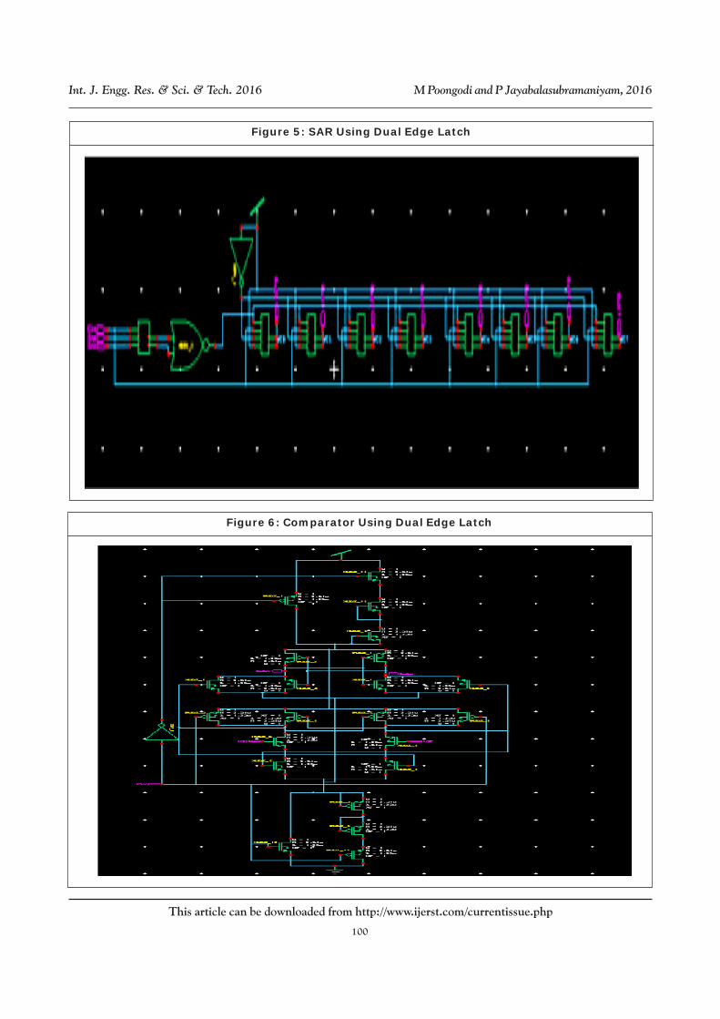
The Successive Approximation is an analog
to digital converter (Figure 5). It consists of
sample and hold circuit to acquire input voltage.
An analog voltage comparator that compares
input to output of internal DAC and outputs the
result of comparison to SAR. A successive
approximation register sub circuit designed to
supply a digital code to internal DAC. An internal
reference DAC comparison with reference
voltage supplies comparator with an analog
voltage equal to digital code output.
A comparator is a device that compares two
voltages or currents and outputs of a digital signal
(Figure 6). It has two analog input terminals and
one binary digital output. It consists of high gain
differential amplifier. It measure digitize analog
CLOCK D Db Q Qb
0 0 1 0 1
1 0 1 0 1
0 1 0 0 1
1 1 0 1 0
Type Pulsed Dual EdgeLatch Latch
Average Power(micro) 7.5320 2.4779
Static Power(milli) 4.7480 2.1584
Static Current(milli) 2.6370 1.1199
Power Delay Product 2.8494 1.0792
Number of Transistors 15 8
Throughput(KHz) 500 200
100
This article can be downloaded from http://www.ijerst.com/currentissue.php
Int. J. Engg. Res. & Sci. & Tech. 2016 M Poongodi and P Jayabalasubramaniyam, 2016
Figure 5: SAR Using Dual Edge Latch
Figure 6: Comparator Using Dual Edge Latch

101
This article can be downloaded from http://www.ijerst.com/currentissue.php
Int. J. Engg. Res. & Sci. & Tech. 2016 M Poongodi and P Jayabalasubramaniyam, 2016
signal such as Analog to Digital Converter (ADC)
and relaxation oscillators.
EXPERIMENTAL RESULTS
Existing Method
The shift register is divided into sub shift registers
to reduce number of delayed pulsed clock
signals. In 4 bit sub shift register four latches store
4 bit data and last latch stores 1 bit temporary
data which will be stored in first latch (Q5) of the
4-bit sub shift register.
Five non-overlap delayed pulsed clock signals
are generated by the delayed pulsed clock
generator. The sequence of the pulsed clock
(Figure 7) signals is in the opposite order of the
five latches. Initially, the pulsed clock signal CLK_
Pulse T updates the latch data T1 from Q4. And
then, the pulsed clock signals CLK_pulse1:4
update the four latch data from Q4 to Q1
sequentially. The latches Q2-Q4 receive data
from their previous latches Q1-Q3 but the first
latch Q1 receives data from the input of the shift
register (IN). The operations of the other sub shift
registers are the same as that of the sub shift
register#1 except that the first latch receives data
from the temporary storage latch in the previous
sub shift register. The proposed shift register
reduces the number of delayed pulsed clock
signal, but it increases the number of latches
because of the additional temporary storage
latches.
Figure 7: Existing Shift Register With Pulsed Latches.

102
This article can be downloaded from http://www.ijerst.com/currentissue.php
Int. J. Engg. Res. & Sci. & Tech. 2016 M Poongodi and P Jayabalasubramaniyam, 2016
GRAPH OUTPUT
PROPOSED METHODDual edge latch is combined with inverter coupling
Figure 8: Proposed Method Dual Edge Latch
circuit (Figure 8). It has two number of transistors
MN1 and MN2. The circuit having two inputs D,Db
and Two outputs Q,Qb. When clock is in “SET”
both MN1, MN2 turns ON when clock is “RESET”
Figure 9: Dual Edge Latch Used in SAR

103
This article can be downloaded from http://www.ijerst.com/currentissue.php
Int. J. Engg. Res. & Sci. & Tech. 2016 M Poongodi and P Jayabalasubramaniyam, 2016
Figure 10: Dual Edge Latch Used in Comparator
MN1, MN2 turns OFF. This dual edge latch (Figure
9) can be used in application of shift registers
such as SAR and COMPARATOR. Dynamic
power, static power, average power can be
reduced. Dual edge latch used fewer amounts of
transistors than shift register with pulsed latches.
The operations of the comparator are two
phase, reset phase and regeneration or evaluation
phase. In the reset phase (Figure 10), the output
nodes are charged to supply voltage or
discharged to the ground depending on the
architecture of comparator. The comparator
tracks the input and regeneration phase the
positive feedback produces the digital value at
the comparator output. The consume power in
regeneration phase and no static power
consumption in reset phase. It introduces large
input offset which makes for high resolution ADC.
This effect can be reduces by increasing the width
of input transistors in differential pair.
CONCLUSIONThe main aim is to reduce area and power by
replacing pulsed latches with dual edge latch. The
average power, static power, dynamic powers are
reduced. The static current and power delay
product has also been reduced. Dual edge
latches combined with inverter coupling circuit.
The circuit having two inputs D, Db and two
outputs Q, Qb. When clock is set MN1 MN2 are
turns ON. When clock is in reset MN1, MN2 turns
OFF. It uses fewer amounts of transistors than
shift register with pulsed latches. It consumes
67% power and 46% area when compared to shift
register with pulsed latches.
REFERENCES1. Chiang S H W and Kleinfelder S (2009),
“Scaling and design of a 16-megapixel
CMOS image sensor for electron
microscopy,” in Proc. IEEE Nucl. Sci.
Symp. Conf. Record (NSS/MIC), pp. 1249–
1256.

104
This article can be downloaded from http://www.ijerst.com/currentissue.php
Int. J. Engg. Res. & Sci. & Tech. 2016 M Poongodi and P Jayabalasubramaniyam, 2016
2. Consoli E, Alioto M, Palumbo G, and Rabaey
J (2012), “Conditional push-pull pulsed latch
with 726 fJops energy delay product in 65
nm CMOS,” in IEEE Int. Solid-State Circuits
Conf. (ISSCC) Dig. Tech. Papers, Feb.
2012, pp. 482–483.
3. Heo S, Krashinsky R, and Asanovic K
(2007), “Activity-sensitive flip-flop and latch
selection for reduced energy,” IEEE Trans.
Very Large Scale Integr. (VLSI) Syst., Vol.
15, No. 9, pp. 1060–1064.
4. Kim S, Yang J H, Park S H, Ryu S T, and
Cho G H (2014), “A 10-bit column-driver IC
with parasitic-insensitive iterative charge-
sharing based capacitor-string interpolation
for mobile active-matrix LCDs,” IEEE J.
Solid-State Circuits, Vol. 49, No. 3, pp. 766–
782.
5. Kong B S, Kim S S, and Jun Y H (2001),
“Conditional-capture flip-flop for statistical
power reduction,” IEEE J. Solid-State
Circuits, Vol. 36, pp. 1263-1271.
6. Partovi H et al. (1996), “Flow-through latch
and edge-triggered flip-flop hybrid elements,”
IEEE Int. Solid-State Circuits Conf. (ISSCC)
Dig. Tech. Papers, pp. 138-139, Feb. 1996.
7. Reyes R, Reviriego P, Maestro J A and
Ruano O (2007), “New protection
techniques against SEUs for moving
average filters in a radiation environment,”
IEEE Trans. Nucl. Sci., Vol. 54, No. 4, pp.
957–964.
8. Stojanovic V and Oklobdzija V (2011),
“Comparative analysis of masterslave
latches and flip-flops for high-performance
and low-power systems,” J. Solid-State
Circuits, Vol. 34, No. 4, pp. 536–548.
9. Teh C K, Fujita T, Hara H and Hamada M
(2011), “A 77% energy-saving 22- transistor
single-phase-clocking D-flip-flop with
adaptive-coupling configuration in 40 nm
CMOS,” in IEEE Int. Solid-State Circuits
Conf. (ISSCC) Dig. Tech. Papers, Feb., pp.
338–339.
10. Yamasaki H and Shibata T (2007), “A real-
time image-feature-extraction and vector-
generation vlsi employing arrayed-shift-
register architecture,” IEEE J. Solid-State
Circuits, Vol. 42, No. 9, pp. 2046–2053.
