int. j. engg. res. & sci. & tech. 2016 a prema and k sedhu .... j. engg. res. & sci....
TRANSCRIPT


85
This article can be downloaded from http://www.ijerst.com/currentissue.php
Int. J. Engg. Res. & Sci. & Tech. 2016 A Prema and K Sedhu Ramalingam, 2016
DESIGN AND ANALYSIS OF LOW POWERPARALLEL SELF TIMED ADDER USING RADIX
METHODA Prema1* and K Sedhu Ramalingam2
The addition of two binary numbers is the fundamental and most often used arithmetic operationon microprocessors, Digital Signal Processors (DSP), and data-processing Application-SpecificIntegrated Circuits (ASIC). Therefore, binary adders are crucial building blocks in Very Large-Scale Integrated (VLSI) circuits. Their efficient implementation is not trivial because a costlycarry propagation operation involving all operand bits has to be performed. Many different circuitarchitectures for binary addition have been proposed over the last decades, covering a widerange of performance characteristics. In this brief, an efficient implementation of asynchronousparallel adder. It is based on Radix method for faster computation of sum and reduced delay. Itis a recursive formulation for performing multi bit binary addition. The computation has beencarried out using parallel processes. Radix-2 is reduce the Power Delay Product (PDP) andEnergy Delay Product (EDP).To obtain low area, the carry is generated first and then it is reusedin sum generation. The adder is Implemented using Tanner tool. The practicality and superiorityof the proposed technique have been verified by simulation.
Keywords: Processor, ASIC, Power Delay Product, Energy Delay Product, Tanner
*Corresponding Author: A Prema [email protected]
1 M.E. (VLSI Design) Student, Sree Sakthi Engineering College, Coimbatore, Tamilnadu, India.2 Assistant Professor, Sree Sakthi Engineering College, Coimbatore, Tamilnadu, India.
Int. J. Engg. Res. & Sci. & Tech. 2016
ISSN 2319-5991 www.ijerst.comVol. 5, No. 1, February 2016
© 2016 IJERST. All Rights Reserved
Research Paper
INTRODUCTIONOver the past few decades, low power design
solution has steadily geared up the list of
researcher’s design concerns for low power and
low noise digital circuits to introduce new methods
to the design of low power VLSI circuits. Moore’s
law describes the requirement of the transistors
for VLSI design which gives the experimental
observation of component density and
performance of integrated circuits, which doubles
every two years. Transistor count is a primary
concern which largely affects the design
complexity of many function units such as
multiplier and Arithmetic Logic Unit (ALU). The
significance of the digital computing lies in the
multiplier design. The multipliers play a significant
role in arithmetic operations in DSP applications.
Recent developments in processor designs also
focus on low power multiplier architecture usage
in their circuits. Two significant yet often
86
This article can be downloaded from http://www.ijerst.com/currentissue.php
Int. J. Engg. Res. & Sci. & Tech. 2016 A Prema and K Sedhu Ramalingam, 2016
conflicting design criteria are power consumption
and speed. Taking into consideration these
constraints, the design of low power multiplier is
of great interest. As reported in Brent (1982), to
get the best power and area requirements of the
computational complexities in the VLSI circuits,
the length and width of transistors are shrunk into
the deep submicron region, handled by process
engineering.
In recent years, the literatures have identified
several types and designs of adiabatic circuits.
For instance, 2N2N2P, PFAL, pass transistor
adiabatic logic, clocked adiabatic l Logic,
improved pass-gate adiabatic logic, and adiabatic
differential switch Logic were designed and
achieved considerable energy savings, compared
with conventional CMOS design (Choudhary,
2008; Cornelius, 2006; Geer, 2005; Govindarajulu,
2008; Kursun, 2002; Liu, 1994; Lo, 1994). In Lynch
(1992), complementary pass transistor adiabatic
logic circuit was discussed, in which the
nonadiabatic energy loss of output loads has
been completely eliminated. In Martin (1992),
adiabatic CPL circuits using two-phase power
clocks were presented. In Maezawa (1997),
energy saving design technique achieved by
latched pass transistor with adiabatic logic was
presented. Many research methods in the
adiabatic logic have been attempted to reduce
the power dissipation of VLSI circuits, reported in
Lo (1994), Lynch (1992), Martin (1992), Maezawa
(1997), Nowick (1996), Rahman (2013), Von
(1966).
Many research efforts in the multiplier design
have been introduced to obtain energy efficiency
in VLSI circuits. A 1.5 ns 32-b CMOS ALU in
double pass-transistor logic was proposed to
improve the circuit performance at reduced
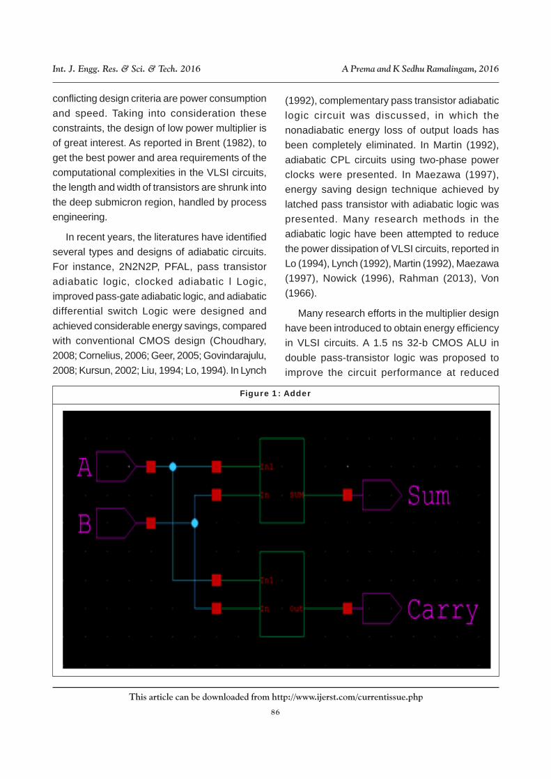
Figure 1: Adder

87
This article can be downloaded from http://www.ijerst.com/currentissue.php
Int. J. Engg. Res. & Sci. & Tech. 2016 A Prema and K Sedhu Ramalingam, 2016
supply voltage ranges. A low power multiplier
using 4-2 compressor based on adiabatic CPL
circuit is described. By the scaling rules set by
Dennard, smart optimization can be achieved by
means of timely introduction of new processing
techniques in device structures and materials. In
Brent (1982), low power multiplier design using
complementary pass transistor asynchronous
adiabatic logic is investigated, which exhibits low
power and reliable logical operations.
ASYNCHRONOUSADIABATIC LOGIC (AAL)Asynchronous adiabatic logic is a unique design
technique which combines the energy saving
benefits of asynchronous logic and adiabatic logic.
Like adiabatic circuits, asynchronous circuits are
also a promising technology to focus on low
power, highly modular digital circuits. One of the
properties of asynchronous systems which make
them useful in these applications is that circuits
include a built-in insensitivity to variations in power
supply voltage, with a lower voltage resulting in
slower operation rather than the functional failures
that would be seen if traditional synchronous
systems were used. Another benefit is the fact
that when an asynchronous system is idle, it will
not utilize clock signals, whereas in synchronous
systems, these clock signals are propagated
throughout the entire system and convert energy
to heat, often without performing any useful
computations.
In contrast to the synchronous circuits,
asynchronous circuits perform handshaking
between their components to perform all
Figure 2: Half Adder

88
This article can be downloaded from http://www.ijerst.com/currentissue.php
Int. J. Engg. Res. & Sci. & Tech. 2016 A Prema and K Sedhu Ramalingam, 2016
necessary synchronization, communication, and
sequencing of operations. Asynchronous circuits
fall into different classes, each offering different
advantages. The main privilege of this circuit is
its low power consumption, stemming from its
elimination of clock drivers and the fact that no
transistor ever transitions unless it is performing
a useful computation.
EXISTING METHODThe architecture and theory behind Asynchronous
Parallel Adder using recursive approach is
presented.
The general architecture of the adder is shown
in Figure 1. Req handshake signal is required for
the selection input for two-input multiplexers from
a single 0 to 1 transition denoted by SEL. During
the initial phase SEL = 0, the actual operands are
initially selected and will switch to feedback/carry
paths for iterative phase using SEL = 1. Multiple
recursions occur through the feedback path and
continue until all the carry values assume zero
values to achieve completion.
The sensor nodes can be communicationeach other without via base station and the sensornetworks application may be one of method orcombine two kinds of methods. For example,CAFEE in categorization of the sensor nodes intomany clusters, and according to the algorithmselect one of clusters head of them. The clustershead will be a management and then the processof the nodes been cluster, then communicationbetween the node and sink. The cluster head is
like a base station.
PROPOSED DESIGNThe main objective of this paper is to design low
power multiplier with energy efficient full adder cell
using double pass transistor with asynchronous
Figure 3: Radix 4 Circuit
89
This article can be downloaded from http://www.ijerst.com/currentissue.php
Int. J. Engg. Res. & Sci. & Tech. 2016 A Prema and K Sedhu Ramalingam, 2016
adiabatic logic. The logic scheme for full adder cell
is illustrated in Figure 1. In this, entire system
consists of two main blocks, such as logical block
and control and regeneration (C&R) block.
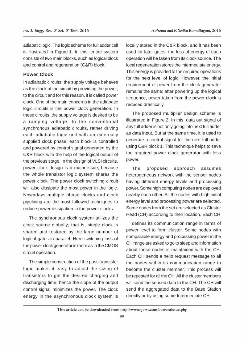
Power Clock
In adiabatic circuits, the supply voltage behaves
as the clock of the circuit by providing the power,
to the circuit and for this reason, it is called power
clock. One of the main concerns in the adiabatic
logic circuits is the power clock generation. In
these circuits, the supply voltage is desired to be
a ramping voltage. In the conventional
synchronous adiabatic circuits, rather driving
each adiabatic logic unit with an externally
supplied clock phase, each block is controlled
and powered by control signal generated by the
C&R block with the help of the logical output of
the previous stage. In the design of VLSI circuits,
power clock design is a major issue, because
the whole transistor logic system shares the
power clock. The power clock switching circuit
will also dissipate the most power in the logic.
Nowadays multiple phase clocks and clock
pipelining are the most followed techniques to
reduce power dissipation in the power clocks.
The synchronous clock system utilizes the
clock source globally; that is, single clock is
shared and restored by the large number of
logical gates in parallel. Here switching loss of
the power clock generator is more as in the CMOS
circuit operation.
The simple construction of the pass transistor
logic makes it easy to adjust the sizing of
transistors to get the desired charging and
discharging time; hence the slope of the output
control signal minimizes the power. The clock
energy in the asynchronous clock system is
locally stored in the C&R block, and it has been
used for later gates; the loss of energy of each
operation will be taken from its clock source. The
local regeneration stores the intermediate energy.
This energy is provided to the required operations
for the next level of logic. However, the initial
requirement of power from the clock generator
remains the same; after powering up the logical
sequence, power taken from the power clock is
reduced drastically.
The proposed multiplier design scheme is
illustrated in Figure 2. In this, data out signal of
any full adder is not only going into next full adder
as data input. But at the same time, it is used to
generate a control signal for the next full adder
using C&R block 1. This technique helps to save
the required power clock generator with less
power.
The proposed approach assumes
heterogeneous network with the sensor nodes
having different energy levels and processing
power. Some high computing nodes are deployed
nearby each other. All the nodes with high initial
energy level and processing power are selected.
Some nodes from the set are selected as Cluster
Head (CH) according to their location. Each CH
defines its communication range in terms of
power level to form cluster. Some nodes with
comparable energy and processing power in the
CH range are asked to go to sleep and information
about those nodes is maintained with the CH.
Each CH sends a hello request message to all
the nodes within its communication range to
become the cluster member. This process will
be repeated for all the CH. All the cluster members
will send the sensed data to the CH. The CH will
send the aggregated data to the Base Station
directly or by using some Intermediate CH.

90
This article can be downloaded from http://www.ijerst.com/currentissue.php
Int. J. Engg. Res. & Sci. & Tech. 2016 A Prema and K Sedhu Ramalingam, 2016
Figure 4: Radix Full Adder Circuit
The purpose of this protocol subjects are
shielded from all time cues, often by a constant
light protocol, by a constant dark protocol or by
the use of light/dark conditions to which the
organism cannot entrain such as the ultra short
protocol of one hour dark and two hours light plays
a vital role in communication and computer
network in which program models the behaviour
of a network by calculating the interaction
between the different network entities using
mathematical formulas. The behaviour of the
network can be observed in a test lab.
EXPERIMENTAL RESULTS
Existing Model
Simulations results Simulation output is to be
obtained by using CADENCE in digital design
environment. The adder was designed using
multiplication technique. In this method usage the
area, power consumption and time are obtained
GRAPH OUTPUTFigure 4 shows the simulation results of parallel
prefix adder. It represents 8 bit hexadecimal
values henceclock is not assigned. The timing is

91
This article can be downloaded from http://www.ijerst.com/currentissue.php
Int. J. Engg. Res. & Sci. & Tech. 2016 A Prema and K Sedhu Ramalingam, 2016
varied for simulation the carry and propagate
values are described for each input and output
values are assigned using the force operation the
run time is varied for each simulation.
Graph Output
The Figure 1 denotes the energy diagram of
existing system. In this system the threshold value
Figure 5: Radix 4 Bit Output
Figure 6: Radix 8 Bit Output
92
This article can be downloaded from http://www.ijerst.com/currentissue.php
Int. J. Engg. Res. & Sci. & Tech. 2016 A Prema and K Sedhu Ramalingam, 2016
only fixed to the node operation. The source node
and destination nodes are automatically
considered. For this node threshold value
decreases the packet losses will be created.
PROPOSED METHOD
Basic Radix-2FA
The main approach in this work is to reduce the
PDP and EDP of an adder and to reduce the
delay due to carry propagation. We use the 24-
transistor mirror FA as a base for our design,
which is illustrated in Figure 3. To optimize the
speed, we joined two FAs in a single block and
use the carry look-ahead technique to shorten
the carry path within the radix-2FA block. The
transistor schematic is shown in Figure 3. The
total transistor count is 56. Boolean equations for
the two carry and two sum gates of the carry-
accelerated design are given below.
The circuit for computing the least significant
sum bit S0 is the same as that of a radix-2 FA.
We use the carry look ahead technique to design
the circuitry for the most significant carry bit Cout.
Equation (5) is similar to the equation for a CLA
with the difference that generate and propagate
signals are generated explicitly for the CLA. To
implement the function that computes the most
significant sum bit S1 with a single gate, we invert
the inputs A1, B1 and C1.
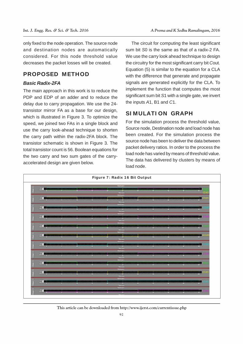
SIMULATION GRAPHFor the simulation process the threshold value,
Source node, Destination node and load node has
been created. For the simulation process the
source node has been to deliver the data between
packet delivery ratios. In order to the process the
load node has varied by means of threshold value.
The data has delivered by clusters by means of
load node.
Figure 7: Radix 16 Bit Output

93
This article can be downloaded from http://www.ijerst.com/currentissue.php
Int. J. Engg. Res. & Sci. & Tech. 2016 A Prema and K Sedhu Ramalingam, 2016
The above graph mentioned to that the energy
of an the source and destination. The value has
been constant in order to using the Load node, it
named as alternate node. This method has
processed to been the packet delivery ratio.
This method has processed to been Energy
value of the Destination node, because of that
alternate node has been changed to that value of
threshold voltage.
CONCLUSIONA parallel prefix adder design is proposed for
overall power consumption. The proposed adder
provides overall area and power than the previous
methods. The parallel asynchronous self timed
adder circuit is efficiently described using a
handshaking protocol and also compared with
other adders proposed adders. The MAC unit is
implemented and the process is achieved
efficiently. Simulation results demonstrate the
effectiveness of the proposed framework in
parallel prefix adder using multiplication through
addition process. The proposed method is
implemented using digital TANNER environment
REFERENCES1. Brent R P and Kung H T (1982), “A regular
layout for parallel adders”, IEEETransaction
on Computer, Vol. 49, No. C-33, pp. 260-
264.
2. Cheng F C, Unger S H and Theobald M
(2002), “Self timed carry- look ahead
Adders”, IEEE Transactions on Computer,
Vol. 49, No. 7, pp. 659–672.
3. Choudhury P, Sahoo S and Chakroborty M
(2008), “Implementation of basic arithmetic
Figure 8: Radix 16 Circuit

94
This article can be downloaded from http://www.ijerst.com/currentissue.php
Int. J. Engg. Res. & Sci. & Tech. 2016 A Prema and K Sedhu Ramalingam, 2016
operations using cellular automaton”,
Proceedings ofInternational centre for
Information Technology, pp. 79–80.
4. Cornelius C, Koppe S and Timmermann D
(2006), “Dynamic circuit techniques in deep
submicron technologies: Domino logic
reconsidered”, in Proceedings of IEEE
International conference on Integrated
circuits design Technology, Vol. 6, pp. 1-4.
5. Geer D (2005), “Is it time for clock less
chips? “Asynchronous processor chips”,
IEEE Computer, Vol. 38, No. 3, pp. 18-19.
6. Govindarajulu S and Jayachandra Prasad
T (2008), “Considerations of Performance
Factors in CMOS Designs”, International
conference on educational development,
Vol. 6, No. 4, pp. 554-562.
7. Kursun V and Friedman E G (2002),
“Domino logic with dynamic body Biased
keeper”, in Proceedings of Solid- State
Circuits Conference. pp. 675–678.
8. Liu W, Gray C T, Fan D, and Far low W J
(1994), “A 250-MHz wave pipelined adder in
2-ìm CMOS”, IEEE Journals on Solid-State
Circuits, Vol. 29, No. 9, pp. 1117–1128.
9. Lo J C (1997), “A Fast Binary Adder with
Conditional Carry Generation”, IEEE
Transactions on Computers, Vol. 46, No. 2,
pp. 248-253.
10. Lynch T and Swartz lander Jr. E E (1992), A
Spanning Tree Carry Look ahead Adder”,
IEEE Transactions on Computers, Vol. 41,
No. 8, pp. 931- 939.
11. Martin A J (1992), “Asynchronous data paths
and the design of asynchronous adder”,
Form. Methods, Vol. 19, No. 4, pp. 119-137.
12. Maezawa M and Polonsky S (1997), “Dual-
rail RSFQ shift register on delay-insensitive
model and its applications”, Technology
Representation of Institute of electronics
Information and Communication
Engineering, Vol. 9, pp. 97-29, and 19-24.
13. Nowick S (1996), “Design of a low-latency
asynchronous adder using speculative
completion”, IEEE Proceedings of
Computer Digital Technology, Vol. 143, No.
5, pp. 301–307.
14. Rahman M Z and Klee man L (2013), “A delay
matched approach for the design of
asynchronous sequential circuits”,
Department of Computer System
Technology International Journal on
Computer, Vol. 29, No. 6, pp. 300-310.
15. Von Neumann J (1966), “The Theory of Self-
Reproducing Automata”, IEEE Transaction
on circuits and system, Vol. 55, No. 8, pp.
171-180.