institute of physics publishing anotechnology 16 the …lsl.postech.ac.kr/data/na5.pdf ·...
TRANSCRIPT

INSTITUTE OF PHYSICS PUBLISHING NANOTECHNOLOGY
Nanotechnology 16 (2005) 2104–2110 doi:10.1088/0957-4484/16/10/022
The selectively manipulated growth ofcrystalline ZnO nanostructuresCongkang Xu, Misuk Kim, Junghwan Chun and Dong Eon Kim1
Department of Physics and Electron Spin Science Center, Pohang University of Science andTechnology, San 31, Hyoja-Dong, Namku, Kyungbuk 790-784, Republic of Korea
E-mail: [email protected] and [email protected]
Received 30 November 2004, in final form 6 July 2005Published 9 August 2005Online at stacks.iop.org/Nano/16/2104
AbstractAligned ZnO nanorods on film, tetrapod nanowires and nanotubes have beenselectively fabricated by a simple one-step route and characterized by x-raydiffractometry (XRD), transmission electron microscopy (TEM),high-resolution TEM (HRTEM) and photoluminescence (PL). PL spectraexhibit different intensity of the green emission relative to the UV emissionfor different nanostructures. The effects of the process parameters ondifferent nanostructures have been discussed. The wettability of well alignednanorods on film was investigated, which reveals a super-hydrophobicity.
1. Introduction
Zinc oxide has been considered one of the most importantmaterials for optoelectronics [1] and piezoelectricity [2]due to its direct wide bandgap (3.37 eV) and non-centrosymmetric structure. In particular, one-dimensionalZnO nanowires have attracted much interest as a consequenceof their remarkable physical and chemical properties. ZnOnanowires have been synthesized by a variety of methodssuch as arc discharge, laser vaporization, pyrolysis, electro-deposition [3–11], metal vapour deposition [12, 13] and metal–organic source vapour deposition methods (MOCVD) [14, 15],template methods [16, 17], vapour transport and condensationmethods [18]. Different ZnO nanostructures may havedifferent applications; for example, the three-dimensionalZnO integrated platform is highly desirable for advancednanoscale electronics and optoelectronics applications [19].The nanowires at the junction of nanowalls will be usefulin energy storage or conversion and data storage andmemory devices [20], well aligned ZnO nanowire arrayshave been applied to a ultra-violet (UV) nanolaser workingat room temperature [3], ZnO quantum wells (QWs) areimportant for application to ultraviolet–blue optoelectronicdevices [21] and intelligent microfluidic switches becauseof their superhydrophobicity [22], and high surface areaZnO nanostructures such as nanotubes [23] can enhancegas sensing and photon-to-electron conversion efficiency aswell as photonic performance. Tetrapod-like nanostructures
1 Author to whom any correspondence should be addressed.
(T-nanowires) could be important for optoelectronics sincethey can be utilized as the fundamental building blocksfor constructing photonic crystals [24]. Much literaturewith respect to ZnO nanostructures is available. However,the shape of nanostructures has not been well controlledyet, not to mention the selectively manipulated growth ofZnO nanostructures without catalyst. Now that the uniqueproperties of nanomaterials depend sensitively on their shapeand size, the invention and innovation of synthetic routesand an insight into the mechanism by which the shapeand size of nanostructures can be easily manipulated is achallenging issue in nanoscience and nanotechnology. In thiscommunication, we have selectively fabricated different ZnOnanostructures such as well aligned nanorod arrays on ZnOfilm, tetrapod-shaped nanowires and nanotubes by controllingprocess parameters. It turns out that this method is verysimple and can be done in one step without catalyst andselectively manipulated to attain different ZnO nanostructures.In particular, the method is favourable for the formation ofnanorods on film. We also investigated the microstructure andoptical properties of different ZnO nanostructures. Moreover,we measured the superhydrophilicity of aligned ZnO nanorodarrays on film.
2. Experiments
Zinc and zinc acetate dihydrate (Zn(C2H3O2)2·2H2O)
powders (Aldrich, 99.999%) were used as the startingmaterials. The synthesis was performed in a conventional
0957-4484/05/102104+07$30.00 © 2005 IOP Publishing Ltd Printed in the UK 2104
The selectively manipulated growth of crystalline ZnO nanostructures
Figure 1. A schematic diagram of the experimental set-up.
(This figure is in colour only in the electronic version)
tube furnace with a horizontal quartz tube (figure 1),where the temperature, pressure, and evaporating time werecontrolled. The detailed process parameters for different ZnOnanostructures are listed in table 1.
Firstly, zinc and zinc acetate dihydrate powders wereloaded into an alumina boat, which was then covered by twopieces of silica wafer with a gap of less than 2 mm. Thepolished faces of the silica wafers were downward. Secondly,the boat was placed in the centre of a quartz tube. High-purity argon gas at a flow rate of 120 sccm was fed into thequartz tube. The furnace was heated to the desired temperature.Maintaining the temperature, the outlet end of the furnace wasopened and air was introduced momentarily into the furnaceonce or several times with a regular interval. After coolingdown the furnace to ambient temperature, the samples wereobtained from the downward polished faces of the wafers.
As-grown samples were characterized and analysed by x-ray diffractometer (XRD, Rigaku D/MAX-IIA) with Cu Kα
(a)
(b)
(c)
(d)
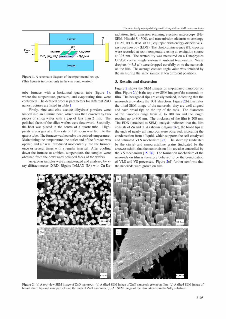
Figure 2. (a) A top-view SEM image of ZnO nanorods. (b) A tilted SEM image of ZnO nanorods grown on film. (c) A tilted SEM image ofbroad, sharp tips and nanoparticles on the ends of ZnO nanorods. (d) An SEM image of the film taken from the SiO2 substrate.
radiation, field emission scanning electron microscopy (FE-SEM, Hitachi S-4300), and transmission electron microscopy(TEM, JEOL JEM 3000F) equipped with energy-dispersive x-ray spectroscopy (EDX). The photoluminescence (PL) spectrawere recorded at room temperature using an excitation sourceat 325 nm. The wettability was measured on a DataphysicsOCA20 contact-angle system at ambient temperature. Waterdroplets (∼3.5 µl) were dropped carefully on to the nanorodson the film. The average contact-angle value was obtained bythe measuring the same sample at ten different positions.
3. Results and discussion
Figure 2 shows the SEM images of as-prepared nanorods onfilm. Figure 2(a) is the top-view SEM image of the nanorods onfilm. The hexagonal tips are easily noticed, indicating that thenanorods grow along the [001] direction. Figure 2(b) illustratesthe tilted SEM image of the nanorods; they are well alignedand have broad tips on the top of the rods. The diametersof the nanorods range from 20 to 100 nm and the lengthreaches up to 800 nm. The thickness of the film is 200 nm.The EDX (attached to SEM) analysis indicates that the filmconsists of Zn and O. As shown in figure 2(c), the broad tips atthe ends of nearly all nanorods were observed, indicating thecondensation from a liquid, which supports the self-catalysedand saturated VLS mechanism [25]. The sharp tip (indicatedby the circle) and nanocrystalline grains (indicated by thearrows) exhibit that the nanorods on film are also controlled bythe VS mechanism [15, 26]. The formation mechanism of thenanorods on film is therefore believed to be the combinationof VLS and VS processes. Figure 2(d) further confirms thatthe nanorods were grown on film.
2105

C-K Xu et al
Table 1. The growth parameters of different nanostructures.
Base Reactionvacuum Temperature chamber Evaporating Air introduction Cooling down(mTorr) (◦C) pressure (Torr) time (min) frequency phase
Aligned 200 650 400 30 per 15 min Arnanorods
Tetrapod 300 700 600 30 0 Airstructures
Nanotubes 95 550 300 mTorr 160 0 Ar
(a)
(b)
Figure 3. (a) An SEM image of T-nanowires on the SiO2 substrate.(b) An SEM image of a T-nanowire with clearly visible steps.
Figure 3(a) shows the SEM images of T-nanowires onSiO2 substrate. The diameter and length of the nanowires are30–200 nm and 1–5 µm, respectively. The steps on the endsof T-nanowires are clearly observed in figure 3(b), resultingfrom the layer-by-layer growth mode, which is consistent withthe available literature on similar hexagon-shape pyramids ofnanocrystalline grains [26].
Figure 4(a) reveals the SEM image of a large number ofnanotubes. Figure 4(b) is a high-magnification SEM image ofthe nanotubes. The diameters of the nanotubes range from 30to 100 nm; the lengths reach a few microns, and the thicknessof the wall ranges from 8 to 15 nm. The upper inset in the imageexhibits the regular hexagonal open tips of ZnO nanotubes. Ananotube with smooth surface is also noticed in figure 4(c).
Figure 5 shows XRD patterns of as-grown nanostructures.The XRD pattern of nanorods on film (figure 5(a)) can beindexed to hexagonal wurtzite ZnO crystal structure withlattice constants of a = 3.248 Å and c = 5.199 Å (JCPDS36-1451). It is noteworthy that the strongest peak is (002),
(a)
(b)
(c)
Figure 4. (a) An SEM image of a large number of nanotubes. (b) Ahigh-magnification SEM image of the nanotubes; the upper inset is ananotube with a hexagonal open end. (c) An SEM image of atypical ZnO nanotube.
implying that the nanorods have preferential growth directionalong [001], which was indicated by hexagonal cross sectionin images of figure 2(a). The XRD pattern of ZnO T-nanowires(figure 5(b)) reveals that the relative strengths of all peaks to
2106

The selectively manipulated growth of crystalline ZnO nanostructures
2 (degree)θ
Rel
ativ
e in
tens
ity (
a.u.
)
Figure 5. (a) An XRD pattern of the nanorods on film. (b) An XRDpattern of T-nanowires. (c) An XRD pattern of the nanotubes.
the background are nearly the same as those of bulk ZnO,manifesting that T-nanowires are good crystallite wurtzitestructure of ZnO with random orientation. Figure 5(c) isthe XRD pattern of nanotubes. The relative strengths of allpeaks to the background in the XRD pattern of the nanotubesare completely different from both nanorods on film and T-nanowires. The (100) peak is noticeably stronger than otherpeaks.
Figure 6(a) shows TEM images of as-prepared nanorodswith broad tips. The diameter of the nanorods is about 50 nm.Figure 6(b) depicts a TEM image of nanorods with sharptips on film. The film is clearly visible and the nanorodsare also well aligned. Figure 6(c) shows a TEM image ofan individual nanorod with a sharp tip. The diameter of thenanorod is about 50 nm. The EDX analysis (the lower inset)indicates that it is composed of Zn and O with the atomicratio of 64 to 36. The SAED pattern (the upper inset) canbe indexed to hexagonal structure ZnO. The nanorod growsalong the [001] direction. Figure 6(d) illustrates an HRTEMimage of the nanorod; the lattice spacing is about 0.26 nm,corresponding to the (002) plane. The long axis of the nanorodwas perpendicular to the (002) plane, indicating that the [001]direction is a common growth direction in ZnO nanorods.Figure 6(e) shows a low magnification of a T-nanowire. Thefourfold twin structure in the central region is clearly visible.Figure 6(f) is a corresponding HRTEM image from the centralregion. It exhibits the structure of the twin boundaries betweenthe neighbouring crystals. As seen from the HRTEM image,the interfaces are distinguished and show no amorphous layer.The twins are conjugated at the boundaries. The inset is thecorresponding FFT.
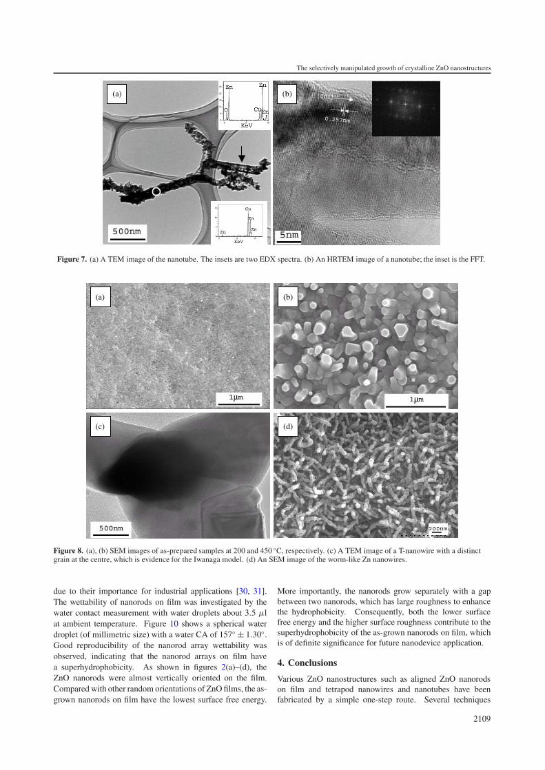
Figure 7(a) is a TEM image of the nanotubes. After thenanotubes had been exposed to the electron beam, they wereseriously damaged. The inset EDX analysis (the upper inset)clearly indicates that the nanotube (as indicated by the blackarrow) consists of Zn and O with the atomic ratio of 78 to22; some of the area (as indicated by the white circle) containspure Zn (the lower inset). Figure 7(b) reveals a high-resolutionTEM image of the nanotube corresponding to the black andwhite in figure 7(a). The interplanar spacing is 0.257 nm,corresponding to the (002) plane of hexagonal ZnO. The inset
Fourier fast transfer (FFT) shows that the nanowire is a singlecrystal.
In order to effectively manipulate the growth of ZnOnanostructures, it is of interest and significance to have aninsight into the formation of various nanostructures. Theformation of ZnO nanorods on film is associated with zincacetate since they were not observed in the absence of zincacetate. Zinc acetate may play a dominant role in the formationof the nanorods on the ZnO film. We investigated ourexperiments carefully so as to support our viewpoint. At200 ◦C only film was observed on silica substrate (figure 8(a)),which is similar to the fabrication of aligned ZnO nanorodsvia a two-temperature-zone furnace [27], which can be utilizedto prefabricate ZnO film via vaporizing zinc acetylacetonatehydrate (Zn(C5H7O2)2·H2O) onto Si substrate at 130–140 ◦C.The present work not only is a one-step procedure but alsofacilitates the formation of nanorods since the growth directionof the nanorods is parallel to that of gravity. When thetemperature reaches the melting point of Zn (419.7 ◦C), thefilm begins to nucleate (figure 8(b)). As the temperature furtherincreases and the time goes on, well aligned nanorod arrayswith broad tips on film are formed. It is noteworthy that thetips are currently broad instead of the conventional sharp shapesince gravity has an effect on the formation of the nanorods asshown in figure 1. The broad tips indicate that the nanorodsare dominated by VLS. On the other hand, both sharp tips andnanoparticles on the hexagonal end of nanorods observed infigure 2(c) manifest that the nanorods are also governed by theVS mechanism. The formation mechanism of the nanorods onfilm is the combination of VLS and VS processes.
Figure 8(c) is the TEM image of an individual T-nanowire. The grain at the centre is probably responsible forthe nucleation and growth of the tetrapod, which is evidencefor the Iwanaga model [24]. Hence, the formation of T-nanowires can be explained by the Iwanaga model. It is knownthat [0001] is the fastest growth direction in the formationof ZnO nanostructures. The octa-twin has four (0001) and(0001̄) surfaces, respectively. Because the (0001) surface ischemically active whereas (0001̄) is inert, the growth along[0001] from the Zn-terminated (0001) surface leads to theformation of a T-shape. The growth mechanism is believedto be the VS process.
The formation of ZnO nanotubes is closely related to lowoxygen atmosphere [22]. Firstly, Zn nanowires are formed toact as an intermediate template and then the surfaces of Znnanowires are oxidized to form ZnO/Zn nanocables. Finally,Zn can be vaporized out of ZnO/Zn nanocables to form tubularstructures. This argument is supported by the experimentdone with a high base vacuum and a lower reaction chamberpressure. As shown in figure 8(d), only pure Zn worm-likenanowires proven by the EDX attached to SEM were obtained.
The PL spectra of the nanorods on film and nanotubeswere measured at room temperature and results are shown infigures 9(a) and (b), respectively. Under the photoexcitationat 325 nm, two PL spectra exhibit narrow and weaker UVemission at 375 nm and a broad stronger green emission bandpeak around 493 nm. UV emission is related to the radiativerecombination of excitons [28], and the green emission tooxygen vacancy [29]. The PL intensity of the green emissionrelative to the UV in nanorods and nanotubes is 3.0 and 11.6,
2107

C-K Xu et al
(a) (b)
(c) (d)
(e) (f)
Figure 6. TEM, EDX and HRTEM images of as-prepared nanorods and T-nanowires. (a) A TEM image of the nanorods with broad tips.(b) A TEM image of the nanorods on the film with sharp tips. (c) A TEM image of an individual nanorod with a sharp tip. The upper andlower insets are its SAED pattern and EDX spectrum, respectively. (d) An HRTEM image corresponding to the nanorods in (c). (e) A TEMimage of T-nanowires. (f) An HRTEM image recorded from the centre of a T-nanowire. Inset is its FFT.
respectively. The intensity of the green emission/UV emissionis related to the concentration of oxygen vacancies and surfacearea ratio. These results show that nanotubes have morevacancy or higher surface to volume ratio than that of nanorodson film.
Wettability is a very important property dominated by boththe chemical composition and the geometrical shape of thesolid surface. The superhydrophobicity surface (with watercontact angle (CA) larger than 150◦) and superhydrophilicitysurface (CA close to 0◦) have been extensively investigated
2108
The selectively manipulated growth of crystalline ZnO nanostructures
(a) (b)
Figure 7. (a) A TEM image of the nanotube. The insets are two EDX spectra. (b) An HRTEM image of a nanotube; the inset is the FFT.
(a) (b)
(c) (d)
Figure 8. (a), (b) SEM images of as-prepared samples at 200 and 450 ◦C, respectively. (c) A TEM image of a T-nanowire with a distinctgrain at the centre, which is evidence for the Iwanaga model. (d) An SEM image of the worm-like Zn nanowires.
due to their importance for industrial applications [30, 31].The wettability of nanorods on film was investigated by thewater contact measurement with water droplets about 3.5 µlat ambient temperature. Figure 10 shows a spherical waterdroplet (of millimetric size) with a water CA of 157◦ ± 1.30◦.Good reproducibility of the nanorod array wettability wasobserved, indicating that the nanorod arrays on film havea superhydrophobicity. As shown in figures 2(a)–(d), theZnO nanorods were almost vertically oriented on the film.Compared with other random orientations of ZnO films, the as-grown nanorods on film have the lowest surface free energy.
More importantly, the nanorods grow separately with a gapbetween two nanorods, which has large roughness to enhancethe hydrophobicity. Consequently, both the lower surfacefree energy and the higher surface roughness contribute to thesuperhydrophobicity of the as-grown nanorods on film, whichis of definite significance for future nanodevice application.
4. Conclusions
Various ZnO nanostructures such as aligned ZnO nanorodson film and tetrapod nanowires and nanotubes have beenfabricated by a simple one-step route. Several techniques
2109

C-K Xu et al
Wavelength (nm)
PL
inte
nsity
(a.
u.)
Figure 9. PL spectra of as-grown nanostructures: (a) nanorods onfilm; (b) nanotubes.
900 µm
Figure 10. Photograph of a water droplet shape on the aligned ZnOnanorods on film.
such as XRD, TEM, HRTEM and PL were employed tocharacterize the as-prepared samples. PL spectra exhibitdifferent intensities of the green emission relative to theUV emission for different nanostructures. The effects ofthe process parameters on different nanostructures have beendiscussed. The well aligned nanorods on film reveal asuperhydrophobicity. This route is believed to selectivelymanipulate the growth of ZnO nanostructures.
Acknowledgments
This project is supported by the electron Spin Science Center(eSSC) funded by the Korean Science and EngineeringFoundation (KOSEF) and the Brain Korea 21 Project in 2004.
References[1] Cao H, Xu J Y, Zhang D Z, Chang S H, Ho S T, Seeling E W,
Liu X and Chang R P H 2000 Phys. Rev. Lett. 84 5584
[2] Wang J S and Lakin K M 1983 Appl. Phys. Lett. 42 352[3] Huang M H, Mao S, Feick H, Yan H Q, Wu Y Y, Kind H,
Weber E, Russo R and Yang P D 2001 Science 292 1897[4] Duan X F and Lieber C M 2000 Adv. Mater. 12 298[5] Konenkamp R, Boedecker K, Lux-Steiner M C,
Poschenrieder M, Zenia F, Clement C L and Wagner S 2000Appl. Phys. Lett. 77 2575
[6] Huang M H, Wu Y Y, Feick H, Tran N, Weber E and Yang P D2001 Adv. Mater. 13 113
[7] Hu J Q, Li Q, Wong N B, Lee C S and Lee S T 2002 Chem.Mater. 14 1216
[8] Li Y, Meng G W, Zhang L D and Phillipp F 2000 Appl. Phys.Lett. 76 2011
[9] Yao B D, Chan Y F and Wang N 2002 Appl. Phys. Lett. 81 757[10] Liu R, Vertegel A A, Bohannan E W, Sorenson T A and
Switzer J A 2001 Chem. Mater. 13 508[11] Kong Y C, Yu D P, Zhang B, Fang W and Feng S Q 2001
Appl. Phys. Lett. 78 407[12] Lyu S C, Zhang Y, Ruh H, Lee H J, Shim H W, Suh E K and
Lee C J 2002 Chem. Phys. Lett. 363 134[13] Tseng Y K, Huang C J, Cheng H M, Lin I N, Liu K S and
Chen I C 2003 Adv. Funct. Mater. 13 812[14] Wu J J and Liu S C 2002 Adv. Mater. 14 215[15] Park W I, Kim D H, Jung S W and Yi G C 2002 Appl. Phys.
Lett. 80 4232[16] Zheng M J, Zhang L D, Li G H and Shen W Z 2002 Chem.
Phys. Lett. 363 123[17] Liu C H, Zapien J A, Yao Y, Meng X M, Lee C S, Fan S S,
Lifshitz Y and Lee S T 2003 Adv. Mater. 15 838[18] Yang P D, Yan H Q, Mao S, Russo R, Johnson J, Saykally R,
Morris N, Pham J, He R R and Choi H J 2002 Adv. Funct.Mater. 12 323
[19] International Technology Roadmap for Semiconductors 2001(San Jose, CA: Semiconductor Industry Association)
[20] Ng H T, Li J, Smith M K, Nguyen P, Cassell A, Han J andMeyyappan M 2003 Science 300 1249
[21] Makino T, Tuan N T, Sun H D, Chia C H, Segawasaki Y,Kawasaki M, Ohtomo A, Tamura K and Koinuma H 2000Appl. Phys. Lett. 77 975
[22] Feng X, Feng L, Jin M, Zhai J, Jiang L and Zhu D 2004 J. Am.Chem. Soc. 126 62
[23] Wu J J, Liu S C, Wu C T, Chen K H and Chen L C 2002 Appl.Phys. Lett. 81 1312
[24] Dai Y, Zhang Y and Wang Z L 2003 Solid State Commun. 126629
[25] Geng C, Jiang Y, Yao Y, Meng X, Zapien J A, Lee C S,Lifshitz Y and Lee S T 2004 Adv. Funct. Mater. 14 589
[26] Kawasaki M, Ohtomo A, Ohkubo I, Koinuma H, Tang Z K,Yu P, Wong G K L, Zhang B P and Segawa Y 1998 Mater.Sci. Eng. B 56 239
[27] Wu J J, Wen H I, Tseng C H and Liu S C 2004 Adv. Funct.Mater. 14 806
[28] Kong Y C, Yu D P, Zhang B, Fang W and Feng S Q 2001Appl. Phys. Lett. 78 407
[29] Vanheusden K, Warren W L, Seager C H, Tallant D K,Voigt J A and Gnade B E 1996 J. Appl. Phys. 79 7893
[30] Parker A R and Lawrence C R 2001 Nature 414 33[31] Erbil H Y, Demirel A L, Avci Y and Mert O 2003 Science 299
1377
2110