information age - bgupaperno/analog_electronics.pdfinformation age: a personal overview ... 1904...
TRANSCRIPT

1
ANALOG DESIGN in the
INFORMATION AGE:
A Personal Overview
ANALOG DESIGN in the
INFORMATION AGE:
A Personal Overview
Barrie GilbertNorthwest LabsPortland, Oregon
Barrie GilbertNorthwest LabsPortland, Oregon
A N A LO GDEVICES

2
OUTLINE OUTLINE A N A LO GDEVICES
A Little Bit of Analog History
The View from ADI’s Ramparts
Old and New Technology Wars
Analog Circuits aren’t What They Seem
Some New Developments
Analog in the Post-Monolithic Age

3
ANALOG TECHNIQUESEMERGED FROM THEFIRST DAYS OF RADIO

4
IN THE CONTEXT OFRECORDED HISTORY,RADIO IS A “NEW” ARTWe are only at the beginning of the history of “wireless” systems, whichdate back only to the beginning of the Twentieth Century.
5
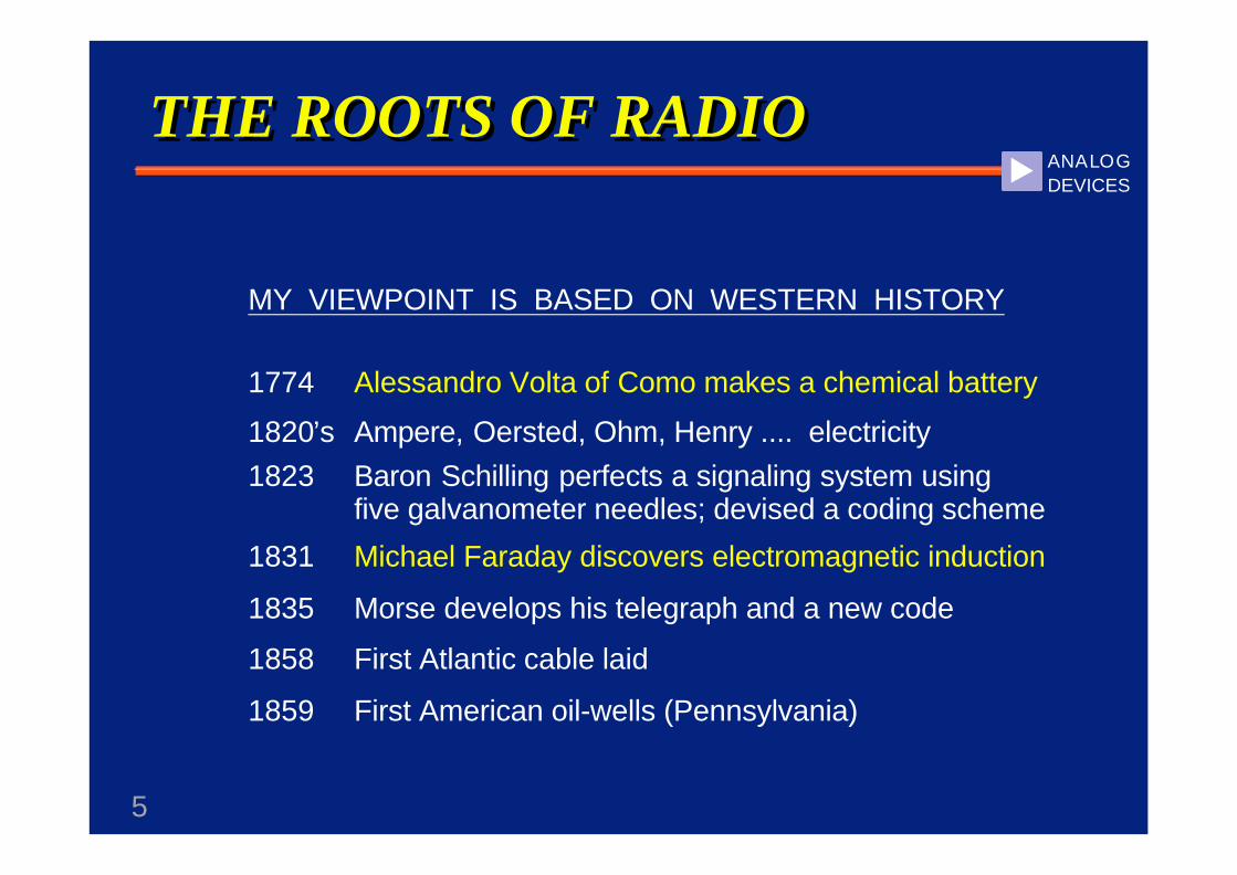
THE ROOTS OF RADIO THE ROOTS OF RADIO A N A LO GDEVICES
MY VIEWPOINT IS BASED ON WESTERN HISTORY
1774 Alessandro Volta of Como makes a chemical battery
1820’s Ampere, Oersted, Ohm, Henry .... electricity
1823 Baron Schilling perfects a signaling system usingfive galvanometer needles; devised a coding scheme
1831 Michael Faraday discovers electromagnetic induction
1835 Morse develops his telegraph and a new code
1858 First Atlantic cable laid
1859 First American oil-wells (Pennsylvania)

6
A N A LO GDEVICES
1861 Johann Philipp Reis made a system to transmit tonesand coined the word “telephone”
Elisha Gray becomes founder of a company that willlater become Western Electric
1867 Nobel invents dynamite; later has regrets
1869 Mendeleyev makes periodic table of elements
THE ROOTS OF RADIO ... cont

7
THE ROOTS OF RADIO ... cont A N A LO GDEVICES
1873 Maxwell publishes his treatise on electromagnetism,a mathematical validation of Faraday’s observationsinterrelating magnetic and electrical phenomena
1876 Bell invents the voice telephone
1877 Edison invents the phonograph
1883 Edison effect noted (a crude thermionic diode)
1884 Paul Nipkow patented first TV system

8
THE ROOTS OF RADIO ... cont A N A LO GDEVICES
1887 Hertz demonstrates electromagnetic waves in Bonn
1888 Tesla’s first alternating current motors/generators
1892 Branly invents the coherer (a crude detector)
1895 Röntgen discovers X-rays
1896 Marconi demonstrates wireless telegraphy over 2km.In the same year, Popov in Russia also sent a wireless message

9
A N A LO GDEVICES
1900 Planck proposes quantum nature of matter
1901 Marconi first transmits across the Atlantic; Bose files patent on a strange microwave detector
1902 Caruso makes first phonograph record
1903 Wright brothers make first aircraft flight
1904 Henry Ford’s factory in first year of business;Fleming invents an improved thermionic diode;Bose’s patent issued (March, USP 755,840)
THE ROOTS OF RADIO ... cont

10
A N A LO GDEVICES
1905 Einstein proposes theory of special relativity
1906 San Francisco earthquake; Rolls-Royce founded
1907 Discovery of blood types; cubism in Paris
1908 First Model-T rolls out of Ford
1909 Blériot makes first flight over English Channel
THE ROOTS OF RADIO ... cont

11
THE FIRST BROADCAST THE FIRST BROADCAST A N A LO GDEVICES
On Christmas Eve, in 1906, Reginald A. Fesseden, at
Brant Rock, Massachusetts, modulated the 1kW output
of a 50kHz alternator, designed by Ernst Alexanderson,
by putting a microphone in series with the antenna!
Electronics 50th Anniversary issue
April 17, 1980, p. 75
In this same year, Lee De Forest invented the “Audion”,
the first vacuum-tube triode.
G. L. Archer, A History of Radio to 1926,
Stratford Press, N.Y., 1938, p. 11

12
WIRELESS GETS SERIOUS WIRELESS GETS SERIOUS A N A LO GDEVICES
1912 Edwin Armstrong first demonstrates “regeneration”
1913 Neils Bohr writes “On the Constitution of Atomsand Molecules”, Philos. Mag., 26, Vol. 1.
1914 Panama canal opens; World World I begins
1918 Armstrong devises the superheterodyne receiver
1920 Regular radio broadcasts begin in USA

13
WIRELESS GETS SERIOUS A N A LO GDEVICES
1925 Lilienfeld proposes a triode device incorporating asemiconductor layer (USP 1,745,175, filed 1928)
1926 Baird invents a practical TV system
1927 The word “Electronics” first appears in a paper byGrondahl & Geiger: “A New Electronic Rectifier”
1930 Sam Weber launches Electronics magazine (April)with contributions from Fleming, Millikan, Goldsmith.
Armstrong conceives of FM (frequency modulation)

14
INTERLUDEINTERLUDEA N A LO GDEVICES
1935 Watson-Watt (UK) and Page (NRL) demonstrate RADAR
1938 First successful magnetron, later smuggled to MIT (1940)
1939 Haeff invents inductive output tube, a forerunner of theklystron (100W CW, 450MHz, 35%, 10dB gain) for TV
1940 Hewlett & Packard open a garage operation in Palo Alto. Later grows to HP

15
INTERLUDEA N A LO GDEVICES
1943 Kompfner invents traveling-wave tube, later perfectedby Pierce and Field at BTL
1944 Analog computers important and in widespread use
1945 Arthur C. Clarke writes “The Space Station: Its RadioApplications”; in October, Wireless World publishes his “Can Rocket Stations give Worldwide Radio Coverage?”
1946 ENIAC developed by Eckert and Mauchly; no thoughtsyet of combining it with a portable radio, however

16
THE TRANSISTOR AGE THE TRANSISTOR AGE A N A LO GDEVICES
1947 (December 16) Brattain and Bardeen (with help) accidentally make a point-contact transistor
1950 Shockley’s “Electrons and Holes in Semiconductors” published by Van Nostrand; alloy junction transistors
1951 Simulated emission in lithium fluoride using RF
1953 First JFETs (Dacey and Ross, Proc. IRE, Vol.. 41)

17
THE TRANSISTOR AGE A N A LO GDEVICES
1954 MASER invented at Columbia University; first International Solid-State Circuits Conference;
first regular color TV service starts in USA
...... and I start work
1957 (May 7) First MOS patent (Ross, USP 2,791,760); models of an IC presented at RRE by Dummer;
Bob Noyce joins Fairchild
1958 Jack Kilby joins TI; by September he’d fabricated a monolithic germanium oscillator and a flip-flop

18
1959: A TRANSITION YEAR 1959: A TRANSITION YEARA N A LO GDEVICES
Kurt Lehovec files patent describing the concept ofjunction isolation (USP 3,029,366, issued April 1962).
The silicon planar technology is developed by Hoerni.
Robert Noyce of Fairchild hears of Kilby’s successes.
Jack Kilby files (February 6) for patent “Miniaturized Electronic Circuits”.
Noyce files (July 30) patent for “Semiconductor Device-and-Lead Structure”.
Shockley having commercial difficulties with his two-terminal (pnpn) switching devices.

19
THE “SOARING SIXTIES”THE “SOARING SIXTIES”A N A LO GDEVICES
1960 Maiman demonstrated first LASER at Hughes Corp.
1961 (March) Fairchild announces its Micrologic family
1962 First semiconductor LASERs and red LED’s arrive
1963 Institute of Radio Engineers merges with the
American Institute of Electrical Engineers to become
the Institute of Electrical and Electronic Engineers
(IEEE); notice that “Radio” is dropped from title
1964 100 transistors integrated in a 5-by-3mm chip (SSI);RCA introduces first production process for MOS.

20
THE “SOARING SIXTIES”A N A LO GDEVICES
1965 Ray Warner moves from Moto to TI, joins Kilby’s team;Tektronix establishes its own in-house Si IC fab.First (successful!) comms-sat (Intelsat-1) operational
1966 Monolithic active mixers, multipliers and current-mode circuits; first issue of Journal of Solid-State Circuits;double-implanted high-frequency pnp transistors
1967 Berkeley develops SPICE; superintegrated circuitsappear, leading to invention of I2L; Carrier Domaindevices first demonstrated

21
THE IC COMES OF AGE THE IC COMES OF AGE A N A LO GDEVICES
1968 Gusev et al. in the Soviet Union fabricated the firstdouble-implanted high-frequency pnp transistors
1969 Ion-implantation used at Mostek (by Sevin); firstmicrowave transistors with Arsenic emitters (Toshiba);1000-transistor logic chips (MSI) become available
1970 Boyle and Smith of Bell Labs announce CCDs;CMOS process is developed at Philips by Shappir;Jobs and Wozniak start Apple Computers

22
THE IC COMES OF AGE THE IC COMES OF AGE A N A LO GDEVICES
1974 First 8-bit microprocessor from Intel
1975 First 10,000-transistor products (VLSI) rolled out
1977 Three mass-market personal computers arrive: the Apple II; Radio Shack's TRS-80; Commodore PET
1980 Apple Macintosh; first camcorders; IBM’s PS/2
1981 IBM unveils their much-awaited PC; HP goes 32-bit

23
CurrentStatus

24
THE “PRODUCTIVITY ENGINE”THE “PRODUCTIVITY ENGINE”A N A LO GDEVICES
Growing IC Markets
Exponential trendsin Technology
and Productivity
Very high R&D andManufacturing
Investments
Chatterjee & Doering, Proc. IEEE, Jan 1998

25
THE “RADIO ROUNDABOUT”THE “RADIO ROUNDABOUT”A N A LO GDEVICES
Growing utilization of spectral window
Escalating numberof radio techniquesand new standards
Push to provideever higher levelsof IC functionality

26
RADIOS ARE FOREVERThey have become a ubiquitous and indispensable aspect of contemporary life, but we’ve only just started. Muchwider use of wireless communication devices is yet to come. Marriage withENIAC appears to be consummated.

27
l AM/FM Radiol Cell phonel Pagerl Car Keysl Radar Detectorl Watch l Garage keyl Collision Avd.l GPSl TV in back

28
ANALOG TECHNIQUESDEVELOPED FROM
1 TELEPHONE2 RADIO3 RADAR4 INSTRUMENTS5 FIRST COMPUTERS

29
ANALOG TECHNIQUESARE IN TRANSITIONThe first one hundred years are now behind us.
The recent marriage between the radio and the computer has led to a new view of design.
New services for radio are in demand, with theemphasis on providing data the most prominent.
Nature’s finite spectrum is now very crowded.
Integrated circuit capabilities and their limitations are shaping many new analog techniques.

30
HOW WILL THEY EVOLVE?HOW WILL THEY EVOLVE?A N A LO GDEVICES
Trends in wireless systems:
l Aggressive cost reduction -- consumable radios?l Greater reliance on bitsl More bandwidth - megadata -- or maybe less: bit-dribblersl Prompt digitization in Rxl Total software flexibilityl Increased use of CMOSl Spread spectrum

31
HOW WILL THEY EVOLVE?A N A LO GDEVICES
Many questions remain:
l Do large mixed-signal analog-plus-digital monolithic SoC’s make sense?l Is System-in-a-Package a better choice?l What changes will occur in the integrated
circuit industry affecting analog design?l Are bipolar transistors still needed?l What is the role of Silicon-Germanium? - or GaAs HBTs, MESFETs, PHEMTs, etc.?
l Spreading the spectrum further: - is operation purely in the time domain practical?

32
SIGNAL FORMSSIGNAL FORMS
t
Time-Domain(UWB)
ClassicalRadio
f
P(f)
t
P(f)
Is Ultra-Wide-Band radio a viable alternative to CW-based radio?Can UWB comfortably co-exist with CW, much like CDMA does?
f

33
AnalogDesignat ADI

34
TECHNOLOGIES at ADI TECHNOLOGIES at ADI
l LEADING-EDGE IN-HOUSE PROCESSES - STRONG HF EMPHASIS inc SiGe
- COMPLEMENTARY BIPOLAR (CB)
- SILICON-ON-INSULATOR (SOI)
- THIN-FILM COMPONENTS
- LASER-TRIMMED CALIBRATION
l CMOS. 0.6, 0.5. 0.35, 0.25 & 0.18µm
- ENHANCEMENTS FOR MIXED-SIGNAL
l SEVERAL GENERATIONS OF BiCMOS
and even CBCMOS
A N A LO GDEVICES

35
ANALOG DESIGN TOOLSANALOG DESIGN TOOLS
l A FULL-TIME CAD TEAM SERVES THE SPECIAL REQUIREMENTS OF THE ANALOG DESIGN COMMUNITY
l PROPRIETARY SIMULATOR (ADICE5) INCLUDES MANY NEW FEATURES
l POWERFUL POST-PROCESSING AND PRESENTATION CAPABILITIES
l PROPRIETARY SCHEMATIC CAPTURE -- all programs linked synergistically
A N A LO GDEVICES

36
ANALOG IC DEVELOPMENTS ANALOG IC DEVELOPMENTS
l TWO KEY THRUSTS
MIXED-SIGNAL SYSTEMS-ON-A-CHIPLarge team efforts; strongly focused on majorsystem initiatives; aimed at providing low-costsolutions; low-power consumption; high-volume
HIGH-PERFORMANCE COMPONENTSSmall-scale of integration; characterized by astrong innovative content; new solutions to oldchallenges; may use “boutique” technologies
A N A LO GDEVICES

37
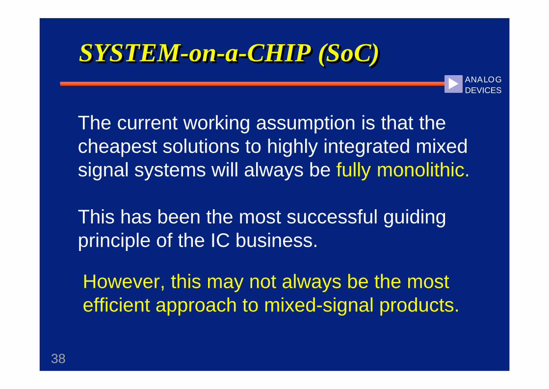
SYSTEM-on-a-CHIP (SoC) SYSTEM-on-a-CHIP (SoC) A N A LO GDEVICES
The current working assumption is that the cheapest solutions to highly integrated mixedsignal systems will always be fully monolithic.
This has been the most successful guidingprinciple of the IC business.
38
SYSTEM-on-a-CHIP (SoC) SYSTEM-on-a-CHIP (SoC) A N A LO GDEVICES
The current working assumption is that the cheapest solutions to highly integrated mixedsignal systems will always be fully monolithic.
This has been the most successful guidingprinciple of the IC business.
However, this may not always be the mostefficient approach to mixed-signal products.

39
SYSTEM-on-a-CHIP (SoC) A N A LO GDEVICES
1. In radios, and other specialized systems,serious challenges stand in the way of integrating sensitive analog sections with “energetic” digital signal sections.
Spurious signal injection; VCO phase-noise disturbances; CMOS inverter-style logic cells are especially troublesome.

40
SYSTEM-on-a-CHIP (SoC) A N A LO GDEVICES
2. Disparate and conflicting demands are placed on a common technology.
For example, while much has been done to utilize submicron CMOS in radio, thereremain many aspects of performance that lie beyond what can sensibly be delivered by a single “one-size-fits-all” technology.

41
SYSTEM-on-a-CHIP (SoC) A N A LO GDEVICES
3. High integration levels -
Reduce the overall die yield - complex chips at the mercy of a few analog cells
Greatly complicate test developmentand production throughput rate
Place immense demands on mixed-signal teams and therefore adversely impact time to market

42
SYSTEM-on-a-HEADER (SoH) SYSTEM-on-a-HEADER (SoH) A N A LO GDEVICES
An alternative path may be the use of smaller die combined into complete systems, using advanced assembly technologies. Critical to the success of this approach will be the use of highly-automated (robot) handling of bare die.
This may be called the “System-on-a-Header”, or“System-in-a-Package” concept.
This can be viewed as simply a natural extension of the manufacturing techniques already widely used in both the electronics and automobile industries.

43
A N A LO GDEVICES
SYNERGY: Optimal IC technologies can be employed
ISOLATION: Critical sections are more readily decoupled
FLEXIBILITY: Systems may be easily configured on demand
VARIETY: Diverse passive components can be included
TEST/YIELD: The ICs are simpler, may be tested separately
TIME-to-MARKET: Can be much quicker than VLSI development
MATERIAL RE-USE: Numerous existing, proven die may be utilized
LOWER RISK: Transferred from large, complex die to simple assembly; mistakes can quickly be corrected
LOWER COST: For many systems, total development cost can be lower than that of a VLSI-SoC
SYSTEM-on-a-HEADER (SoH)

44
SYSTEM-on-a-HEADER (SoH) A N A LO GDEVICES
The use of highly-automated assembly techniques, in which a broad variety of optimal technologies are synergistically combined, will herald a new phase in the evolution of mixed-signal electronics. It will soon be common to expect that the highest performance, quickest time to market, and lowest development cost will be achieved through multi-chip methods.
We are at the beginning of the
“POST-MONOLITHIC ERA”

45
But TechnologyWars are StillBeing Fought!

46
TECHNOLOGY WARSTECHNOLOGY WARSA N A LO GDEVICES
DIGITAL! versusANALOG?

47
A N A LO GDEVICES
DIGITAL! versusANALOG?
New! Better!
The Future!Superior!
Advanced!
Tired
OldStale
Obsolete
Unstable
TECHNOLOGY WARS

48
A N A LO GDEVICES
Everyone knows that analog is “old stuff ”.It’s unreliable, prone to drift and noise, itgoes out of calibration. It’s where all thetroubles are found in any equipment.
Communications systems will very soon be entirely digital.
TECHNOLOGY WARS

49
A N A LO GDEVICES
TECHNOLOGY WARS
Everyone knows that analog is “old stuff ”.It’s unreliable, prone to drift and noise, itgoes out of calibration. It’s where all thetroubles are found in any equipment.
Communications systems will very soon be entirely digital.
Nothing could be farther from the truth.

50
A N A LO GDEVICES
1. Digital modulation has immense advantages (data compression and spectral efficiency; use of error-correcting codes; ubiquity of digital data)
2. Digitization at the earliest point in a receiver allows the use of very powerful DSP filtering
3. Some bulky analog filters can be eliminated
4. Similar kinds of benefits arise in transmitters
5. Software control of channel frequency, gain, power control and other critical parameters makes radio a “computer peripheral”
BENEFITS of “DIGITAL” RADIOBENEFITS of “DIGITAL” RADIO

51
A N A LO GDEVICES
6. Leads to the development of fully-programmable transceivers (the “universal” or “software” radio)
7. Makes possible the use of sophisticated techniques such as CDMA, even pure time-domain methods, in which complex coding and decoding is needed
8. The overall management of cellular, satellite, cable and fibre networks would be impossible without complex digital supervision
9. Leads to more innovative use of deep sub-micron CMOS technologies and “digitally-friendly” circuit techniques (such as sigma-delta converters) in what were formerly strictly analog domains
BENEFITS of “DIGITAL” RADIO

52
NEVERTHELESS ...NEVERTHELESS ...A N A LO GDEVICES
A There is little likelihood of finding ways to totally dispense with analog techniques in many areas of modern electronic systems of all kinds.
B Examples include: power sources; amplification;many kinds of HF filtering; microwave mixers and modulators; HF power generation; high-accuracy measurement devices in medical instruments aswell as in radio; numerous kinds of VCOs forcarrier and reference frequencies; new photonicinterfaces and support of optical elements; etc.
C Analog signal processing can often provide asignificant reduction in complexity (it is “elegant”).

53
SO..... WHAT IS THE ROLE OF ANALOG in the INFORMATION AGE?
SO..... WHAT IS THE ROLE OF ANALOG in the INFORMATION AGE?
It is a matter of common knowledge that electronicshas radically changed in character since the advent of the microprocessor.
Analog techniques really have become a less centralaspect of modern electronics, even to the point whereit is believed by many they are no longer important.
Few young people pursue analog design as a hobby; simple, basic materials are often hard to acquire.

54
A SENSIBLE SYNERGYA SENSIBLE SYNERGYA N A LO GDEVICES
DIGITAL!teaming with
ANALOG!

55
Why isAnalog Design
“So Hard”?

56
QUESTIONSQUESTIONSA N A LO GDEVICES
? Why is analog design so often regardedas especially difficult by new graduates?
? Will there be enough analog designers inthe work force when the “first generation”(those trained during World War II years)have all gone? Where will they come from?
? What can be done in universities to ensurethat classical concepts in electronics and the linear signal-processing topics are notneglected in the curriculum?

57
Analog circuits are more intimately a part of the physical world than are digital processors, since they are concerned with manipulation of signals having DIMENSION. Their physical attributesare traceable directly to fundamental quantities and constants, governing all real systems:
LENGTH: [L] Meter MASS: [M] KilogramTIME: [T] SecondCHARGE: [Q] Coulomb
ASPECTS of ANALOG DESIGNASPECTS of ANALOG DESIGN

58
LENGTH: [L] Meter MASS: [M] KilogramTIME: [T] SecondCHARGE: [Q] Coulomb
Dimensional signals:
VOLTAGE: [MLT2L-2Q-1] VoltCURRENT: [QT-1] AmperePOWER: [ML2T-3] WattFREQUENCY: [T-1] Hertz
Dimensional elements:
RESISTANCE: [ML2T-1Q-2] OhmCAPACITANCE: [M-1L-2T2Q2] FaradINDUCTANCE: [ML2Q-2] Henry

59
ANALOG DESIGN DIFFERS FUNDAMENTALLYFROM DIGITAL DESIGN MAINLY BECAUSE ITIS AN INSEPARABLE PART OF THE PHYSICAL WORLD. IT IS “NEWTONIAN”.
DIGITAL LOGIC USES ELECTRONICS BECAUSESILICON ALLOWS THE FABRICATION OF FASTAND COMPLEX ALGORITHMIC ENGINES AT VERY LOW COST. IT IS ONLY INCIDENTALLY ELECTRONIC. DIGITAL DESIGN IS NOT OFTEN CONCERNED WITH CRITICAL CIRCUIT ISSUES.
THE “BIG DIFFERENCE”THE “BIG DIFFERENCE”A N A LO GDEVICES

60
THE “BIG DIFFERENCE”A N A LO GDEVICES
ANALOG CIRCUIT DESIGN INVOLVES VERY FEW COMPONENTS, YET THESE CAN LEAD TO VERY COMPLEX MATHEMATICS. THIS ISESPECIALLY TRUE WHEN ALL NONLINEAREFFECTS ARE CORRECTLY INCLUDED.
NUMEROUS SUBTLE MECHANISMS MATTERBUT THEY ARE OFTEN NOT ADDRESSED INTEXTBOOKS: FOR EXAMPLE, THE EFFECTSOF VARACTOR PARASITIC CAPACITANCES IN RF AMPLIFIERS.

61
ANALOG ARRAY PROCESSORANALOG ARRAY PROCESSOR
Iw1 Iw2 Iwk IwN
Iy
Ix1 Ix2 Ixk IxN
Iwk = Ixk IyΣk
Ixk
A N A LO GDEVICES

IX IYIZ
IZ = √ IX
2 + IY2
VECTOR SUMMATIONVECTOR SUMMATIONA N A LO GDEVICES
(INPUT)(OUTPUT)
(INPUT)

63
THE “BIG DIFFERENCE”A N A LO GDEVICES
TOPOLOGICAL (COMBINATORIAL) RICHNESS OF SIMPLE ANALOG CIRCUITS QUICKLY LEADS TO EXPLOSIVE VARIETY.
FOR EXAMPLE, THERE ARE TWENTY-FOURDISTINCTLY DIFFERENT CIRCUITS THAT CAN BE DEVISED USING ONLY TWO TRANSISTORS!
BY THE TIME THREE OR FOUR TRANSISTORSARE USED, THE NUMBER OF COMBINATIONSBECOMES HUNDREDS.

64
THE “BIG DIFFERENCE”A N A LO GDEVICES
TOPOLOGICAL (COMBINATORIAL) RICHNESS
... cont
NOT ONLY ARE THE NUMBER OF DIFFERENTCIRCUITS VERY LARGE BUT THE BEHAVIOURQUICKLY BECOMES COMPLICATED AND MAYNOT BE READILY APPARENT BY INSPECTION

KERMIT_6
IOUT = I1 − I6
Q1 Q3 Q4
VIN−VIN+
+I1 I6
This is a very linear transconductance whose magnitude is proportional to IT
IT
33e14e2e
Q1 Q5 Q6
33e 14e 2e
1 2.9 4.7 2.9 1
A N A LO GDEVICES

A N A LO GDEVICES
VIN
Output CurrentsI1 I6
VERY LINEAR CLASS-AB BEHAVIOURgm constant to within ±0.05dB to VIN = ±0.65V
2% of IT
gm

67
PARAMETRIC SLAVERYPARAMETRIC SLAVERYA N A LO GDEVICES
The deeply-physical nature of analog circuits places quite different demands on a manufacturing process to those needed for the fabrication of digital circuits, primarily due to the unavoidable dependence on the absolute values of numerous parameters.
Achieving design robustness – which requires thesystematic elimination (or at least, the minimization)of sensitivities to all process parameters – posesunique challenges. Design for Manufacture in theanalog world demands unrelenting attention to avery large number of small details.

68
PARAMETRIC SLAVERY A N A LO GDEVICES
This is commonly known as the PVT challenge –Process, Voltage and Temperature must all bemade to have minimum impact on performance.
Sound design practice, including careful choicesof product architecture and technology, and cell topology, can lower the risk of parametric failures. But thorough simulation of the full range of PVT conditions is essential in analog practice, and invariably this work is extremely time-consuming.
It also requires excellent device modeling, to a fargreater extent than needed for digital design.

69
PARAMETRIC SLAVERYA N A LO GDEVICES
Thus, using the CAD model libraries for the “fast”,“slow”, and “nominal” device models (of all kinds,not only transistors), and operating temperaturesof, say, –60°C, 30°C and 120°C one generates aset of nine results; repeating at a supply voltage of, say, 2.6V, 3V and 3.6V requires twenty-sevensimulation runs, for each of perhaps fifty or morekey performance aspects. Any time a change ismade in the design – even a small one – these must be repeated all over again.
70
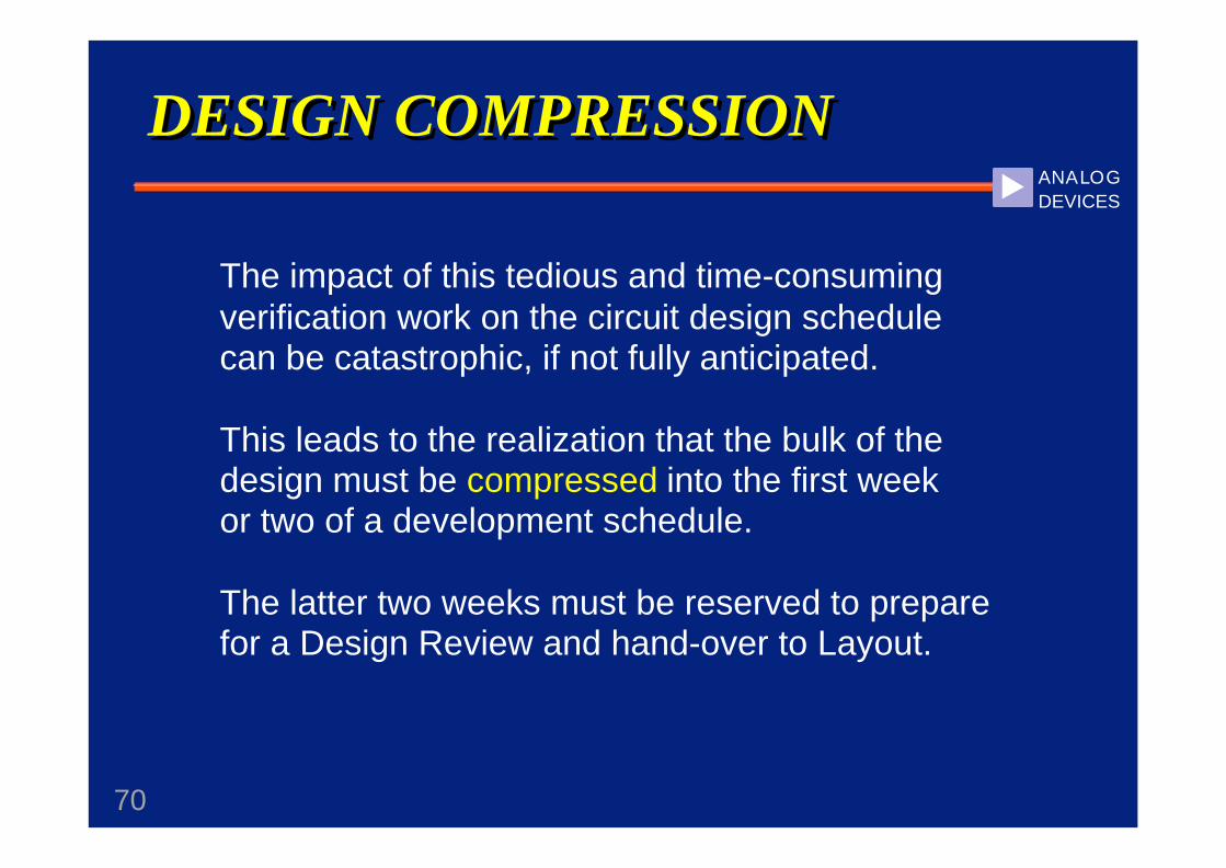
DESIGN COMPRESSIONDESIGN COMPRESSIONA N A LO GDEVICES
The impact of this tedious and time-consumingverification work on the circuit design schedule can be catastrophic, if not fully anticipated.
This leads to the realization that the bulk of thedesign must be compressed into the first week or two of a development schedule.
The latter two weeks must be reserved to preparefor a Design Review and hand-over to Layout.

71
BACK EXTRACTIONBACK EXTRACTIONA N A LO GDEVICES
Only after the IC layout has been completed canthe capacitances of interconnections, and some of their resistances, be extracted and added back into a new set of simulation studies, which need to be just as thorough as those during pre-layout.
These parasitics (along with others, for example,the package reactances and ESD protection) areof pivotal importance in RF-IC design. Experienceteaches that the behavior of almost any circuit willbe radically different when they are included. Timeis thus needed to pursue further remedial action.

72
NEW ANALOG FRONTIERS NEW ANALOG FRONTIERS A N A LO GDEVICES
Fiber systems have heralded a return to many basicphysical principles and device development, beingessentially “Newtonian”, as are RF systems:
l Dispersion compensation in optical fibers
l All-optical erbium-doped fiber amplifiers
l Multi-wavelength channel splitters
l Power-sampling partial splitters
l Laser-diode drivers and modulators
l Micromechanical (MEM) multiplexers
l Supervisory functions of many kinds

73
ANOTHER “WAR”ANOTHER “WAR”A N A LO GDEVICES
BIPOLAR? versus
squeak
fizz
CMOS!CMOS!

74
XFCB BIPOLAR TECHNOLOGIES XFCB BIPOLAR TECHNOLOGIES
l Ultra-Low Inertia:
Small transit time and low capacitances
Substrate capacitance not a varactor
l Trench-Isolated; Bonded Wafers (SOI)
l Three processes in full production
l Laser-trimmable thin-film resistors
l High-quality metal-plate capacitors
l Excellent device modeling
A N A LO GDEVICES
HIGH-PERFORMANCE COMPLEMENTARY BIPOLAR

75
WHY CONTINUE TO BE CONCERNED
WITH BJT’S − WHEN AN INCREASING
NUMBER OF MODERN SYSTEMS ARE
TURNING TO CMOS TECHNOLOGIES
FOR RF SIGNAL PROCESSING?A N A LO GDEVICES

76
Audio Interface/Processing
Audio Interface/Processing BasebandBaseband RF/IFRF/IF
CodecsDSP
Mixed-Signal
A/D & D/AConvertersAmplifiers
MixersModulatorsLNAs, VGAsVCO/Synth
BSC/PSTN
BSC/PSTN
Highest Performance Devices willContinue to use BJT TechnologiesHighest Performance Devices willContinue to use BJT Technologies
Log Amps &other RF M&C
A N A LO GDEVICES
A N A LO GDEVICES

77
Audio Interface/Processing
Audio Interface/Processing BasebandBaseband RF/IFRF/IF
CodecsDSP
Mixed-Signal
A/D & D/AConvertersAmplifiers
MixersModulatorsLNAs, VGAsVCO/Synth
BSC/PSTN
BSC/PSTN
Highest Performance Devices willContinue to use BJT Technologies
Log Amps &other RF M&C
A N A LO GDEVICES
A N A LO GDEVICES
CMOS territory
BJT, HBT,MESFETs

78
Audio Interface/Processing
Audio Interface/Processing BasebandBaseband RF/IFRF/IF
CodecsDSP
Mixed-Signal
A/D & D/AConvertersAmplifiers
MixersModulatorsLNAs, VGAsVCO/Synth
BSC/PSTN
BSC/PSTN
Highest Performance Devices willContinue to use BJT Technologies
Log Amps &other RF M&C
A N A LO GDEVICES
A N A LO GDEVICES
LOGICAL,ALGORITHMS
NEWTONIAN

79
BJT MODELINGBJT MODELINGCONTRARY TO SOME VIEWPOINTS, THE BJT
IS FAR EASIER TO DESCRIBE IN MODELING
EQUATIONS, COMPARED TO CMOS. WHILE
THE EQUATIONS ARE STILL COMPLEX, THEY
ARE FUNDAMENTALLY SOUND, OVER A VERY
WIDE RANGE. USING SOI SUBSTRATES, THE
BJT IS A PURE, THREE-TERMINAL DEVICE; ITS
TINY COLLECTOR-SUBSTRATE CAPACITANCE
IS NOT VOLTAGE-DEPENDENT. THERE ARE
NO OTHER SUBSTRATE SENSITIVITIES.A N A LO GDEVICES

80
ADVANCED MODELSADVANCED MODELS
FOR MANY MICROWAVE APPLICATIONS IT IS
NECESSARY TO INCLUDE SPECIAL ASPECTS
OF BJT DEVICE BEHAVIOR. EXCELLENCE IN
THIS ARENA, CENTERED ON IN-HOUSE CAD
TEAMS, PROVIDES A MAJOR COMPETITIVE
ADVANTAGE. FOR EXAMPLE, THE BJT SUPER-
MODELS INCLUDE DISTRIBUTED ASPECTS
OF DEVICE BEHAVIOR. NUMEROUS OTHER
SUBTLE DETAILS ARE GENERALLY NOT OF
IMPORTANCE AT LOWER FREQUENCIES.A N A LO GDEVICES

81
HOWEVER . .HOWEVER . .
DEEP SUB-MICRON CMOS PROMISES
TO PROVIDE SOME PERFORMANCE
ADVANTAGES (BETTER LINEARITY,
ABSENCE OF SHOT NOISE) THOUGH
NOT YET FULLY PROVEN; DIE COST
IS RARELY OF MATERIAL CONCERN
IN SSI AND EVEN LSI RF PRODUCTS
A N A LO GDEVICES

82
HOWEVER . .
MANY OF THESE BJT CELL DESIGNS
HAVE ALREADY BEEN ADAPTED TO
CMOS FORM, AND IN GENERAL THE
THEORY IS DIRECTLY APPLICABLE;
THE “GAP” BETWEEN BJT AND CMOS
DESIGN PARADIGMS IS NARROWING
A N A LO GDEVICES

83
HOWEVER . .
IN ULTRA-SHORT-CHANNEL CMOSTRANSISTORS (BELOW 0.2µm) THESUBTHRESHOLD REGION EXTENDS UP TO CURRENTS AT WHICH QUITEHIGH fT’s ARE POSSIBLE, WHEN
CMOS è BJT
A N A LO GDEVICES

84
l PRESENT-DAY (0.35-0.18µm) CMOSDEVICES STILL HAVE LOWER gm/CRATIOS THAN COMPARABLE BJTs
l LOW-FREQUENCY NOISE AN ISSUEl NONLINEAR OUTPUT CONDUCTANCE
- can quickly lose that nice gm linearity at the load
l MANY SUBSTRATE SENSITIVITIESl EXTREMELY COMPLEX BEHAVIOURl CONSEQUENTLY, POOR MODELING
CMOS SHORTFALLCMOS SHORTFALL
A N A LO GDEVICES

85
A BITAbout
the BJT

... this was the commonplace view of how the transistor works
R
BASEBATTERY
i C = β i B
50 YEARS AGO 50 YEARS AGO
COLLECTOR
BATTERY
i B
A N A LO GDEVICES

R i B
i C = β i B
COLLECTOR
BATTERY
50 YEARS AGO
The Beta View
BASEBATTERY
... this was the commonplace view of how the transistor works
A N A LO GDEVICES

BUT LOOK CLOSER ........BUT LOOK CLOSER ........
?
A N A LO GDEVICES

THE BJT AT HIGH MAGNIFICATIONTHE BJT AT HIGH MAGNIFICATION
A N A LO GDEVICES

l IC = IS(T) exp VBE / VT
l VBE = VT log IC / IS(T)
l ONE EQUATION; TWO FORMS
A N A LO GDEVICES
THE HEART OF THE BJTTHE HEART OF THE BJT

TRANSCONDUCTANCE TRANSCONDUCTANCE
l IC = IS(T) exp VBE / VT
l dIC / dVBE = IS(T) exp VBE / VT / VT
l gm = IC / VT
l WHICH IS LITTLE SHORT OF MIRACULOUS!A N A LO GDEVICES

MULTIPLICATION USING A SLIDE-RULE
MULTIPLICATION USING A SLIDE-RULE
x
y
20 5
1 10 100 1000
1 10 100 1000
Length ∝ 100
SCALE ‘A’
SCALE ‘B’
A N A LO GDEVICES

MULTIPLICATION USING TRANSISTORS
MULTIPLICATION USING TRANSISTORS
Ix
Iy
Vx ∝ log Ix
Vy ∝ log Iy
Vz ∝ log IxIy
A N A LO GDEVICES

THE ‘BAND-GAP’EQUATION FOR VF(IF,T)
THE THE ‘‘BAND-GAPBAND-GAP’’EQUATION FOR VEQUATION FOR VFF(I(IFF,T),T)
VF = EGE - HVEN - VTN (log - η log H )IF
IN
where H is the ‘Hotness factor T/ TN
VEN = EGE - VNa temperature-independentconstant for a given device
A N A LO GDEVICES

VF versus TEMPERATURE VF versus TEMPERATURE
EGE ~ 1.2V
T (K)0
0
THE SLOPE IS DETERMINEDBY THE CURRENT DENSITY
300K
~ 0.6V
VF
A N A LO GDEVICES

96
> Exploits a fundamental and unique property of the bipolar transistor Transconductance (gm) is reliably a linear function of collector current:
gm = IC / VT where VT = kT/q
> The basis of almost all analog multipliers and numerous VGAs since the late ’60’s
> Current-mode signal processing is often used
TRANSLINEAR DESIGNTRANSLINEAR DESIGNA N A LO GDEVICES
A N A LO GDEVICES

97
> In short, the bipolar transistor retains certain unique properties not matched by any CMOS technology, in particular, the remarkable benefits of “translinearity”.
> In many difficult areas of wireless systems, the BJT(or its more sophisticated cousin, the HBT) provides significant performance advantages over CMOS, for example, in low-noise amplifiers and power amplifiers (where GaAs HBTs are proving valuable).
> The highly predictable and mathematical nature of the bipolar transistor can be relied on to provide very high levels of accuracy and temperature stability.
TRANSLINEAR DESIGNA N A LO GDEVICES
A N A LO GDEVICES

98
ANALOG DESIGN in theINFORMATION AGE must use
PARTNERSHIPS of TECHNOLOGY
ANALOG DESIGN in theINFORMATION AGE must use
PARTNERSHIPS of TECHNOLOGY
ANALOG teaming with DIGITAL
BIPOLAR teaming with CMOS
SOC’s teaming with SOH’s
A N A LO GDEVICES

99
Some BJT“Tricks”

CLASSIC MIXERCLASSIC MIXER
LO
RF
IF
BIAS
Gm

LO
RF
ZIN ?
ZOUT ?
DC LEVELS ? NOISE ?
LINEARITY ?
LO FEED-THROUGH ?
CLASSIC MIXERIF
BIAS?
DEVICESIZES ?

LO
RF
LINEARITY ?
CLASSIC MIXERIF
(it is good enough?how good is good enough?how is it improved?)

103
> A special class of translinear circuit, which does not invoke current-mode techniques
> Achieves reductions in distortion through the use of a multiplicity of tanh functions
> Very effective in certain circumstances> Once an academic curiosity, multi-tanh
cells are now widely used
The ‘MULTI-tanh’ TECHNIQUEThe ‘MULTI-tanh’ TECHNIQUEA N A LO GDEVICES

104
MT-DOUBLET in a MIXERMT-DOUBLET in a MIXER
RF INPUT
Q1
Q2
Q3
Q4Ae
Aee
e
A N A LO GDEVICES
LO INPUT

SUMMATION OF THETWO tanh SECTIONS
SUMMATION OF THETWO tanh SECTIONS
+ IT
- IT
IOUT
VRF
VTlog Α
-VTlog Α 2
1
1 + 2

106
INCREMENTAL GAIN of DOUBLETINCREMENTAL GAIN of DOUBLET
VIN= 0
À + Á
À Á
VIN= +6VTVIN= -6VT
VINExample, for Α = 4
A N A LO GDEVICES

ΑΑ1 2 3 4 5 6 7
-90
-100
-110
-120
-130
-140
0-1-2-3-4-5-6-7
Doublet: Relative Gain and HD3 vs. ΑDoublet: Relative Gain and HD3 vs. Α
dBdB
dBdB
1mV input1mV input
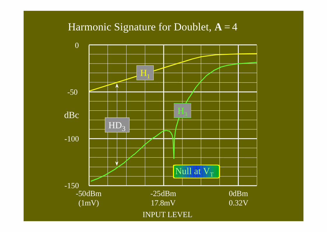
0dBm0.32V
-25dBm17.8mV
-50dBm(1mV)
INPUT LEVEL
Harmonic Signature for Doublet, Α = 4
-150
-100
-50
0
dBc
Null at VT
H1
H3
HD3

109
ACHIEVING LINEAR-in-dB GAINACHIEVING LINEAR-in-dB GAIN
+
Me RB
RG e
QD
QE
IP
IG
PRIMARY BIAS (PTAT, typ. 100µA)
GAIN-CONTROL BIAS(PTAT, typ. 0 to 50µA)
RF/IFINPUT
gm CELL IOUT
Q1
Q2
QB
MIP exp-VG
VT
VG
- +
VG = 2.98mV/dB @ 300K
IT
A N A LO GDEVICES

110
Q1
Q2 Q4 Q6Ae
Ae
Q3 Q5
RF/IFINPUT
e e
e e
IOUT
MULTI-tanh TRIPLETMULTI-tanh TRIPLETA N A LO GDEVICES
KI II

1 + 3 + 2
VX= +100mVVX= -100mV A = 13, K = 3/4
INCREMENTAL gmof a typical TRIPLETINCREMENTAL gmof a typical TRIPLET
±0.043dB@ ±56mV
21 3

Harmonic Signature for Triplet, A=13, K=3/4
-150
-100
-50
0
dBc
ω
3ω
0dBm0.32V
-25dBm17.8mV
-50dBm(1mV)
A N A LO GDEVICES

113
+Q1
Q2
MULTI-tanhTRIPLET
Q4 Q6
RE
Ae
Ae
Q3 Q5
RE RB
QA QB QC
Ne Me Ne
RF/IFINPUT
CDEC
RG
e
e e
e e
QE
IOUT
IP
IG
PRIMARYBIAS
GAINBIAS
TRIPLUS: MULTI-tanh TRIPLET+TRIPLUS: MULTI-tanh TRIPLET+A N A LO GDEVICES
THIS SPECIAL BIASING SCHEME EXTENDS DYNAMIC RANGE

114
CURRENT IN INNER gm PAIR- PERFECTLY EXPONENTIAL
3mA
2mA
1mA CURRENTS IN OUTER gm PAIRS; NOT EXPONENTIAL
RATIO = N/M
INCREASING IGIG=0
BIAS CURRENTS in INNER/OUTER gm CELLSBIAS CURRENTS in INNER/OUTER gm CELLSA N A LO GDEVICES
INCREASING GAIN

115
-5
0
5
10
15
20
25
30
-100 -80 -60 -40 -20 0 20 40 60 80 100
VIN in mVP
dB
TRIPLUS Incremental Gain vs. Instantaneous VINTRIPLUS Incremental Gain vs. Instantaneous VIN
MAX. GAIN
MIN. GAIN

Harmonic Signature for an Optimized Quadlet
-150
-100
-50
0
dBc
0dBm0.32V
-25dBm17.8mV
-50dBm(1mV)
EH3
ω
3ω
-40dBm3.2mV
HD3 = - 80DdBc
A N A LO GDEVICES

ZIN
LO
RF
IF
I0
MICROMIXERMICROMIXER
IZ
e
e
Me
Me
Me

ZIN IZ
BIAS CURRENTUNIQUELY
DETERMINESIMPEDANCE
LO
RF
IF
MICROMIXER

3p
Q1
Q2
Q3
VLO
QM1 QM2 QM3 QM4
VRF 2.5p10p2k
12n
12n
12n
16e
1.18mA 1.18mA
16e
16e 20p
8p
2k 8k 8k
1k
8k
15k 10k
0V
86µA 68µA 60µA 94µA
94µA132µA94µA
QB1e
e 12e
QB2 QB3
2.3V min.
QB4
3e
QB5
16e
50Ω @1.6GHz
IIF
L-BAND MICROMIXER

120
Log-Amps

121
A N A LO GDEVICES
“LOG-AMPS” ARE NONLINEAR CIRCUITS WHICHCONVERT A WIDE-DYNAMIC RANGE SIGNAL ONA DECIBEL SCALE TO A QUASI-DC VOLTAGE OFSMALL RANGE: -70dB to 0dB becomes 0 to 1.4V.
WHEN DESIGNED WITH SUFFICIENT CARE TOPROVIDE CALIBRATED OPERATION, THEY AREHIGHLY VALUABLE MEASUREMENT DEVICES.
LOGARITHMIC AMPLIFIERSLOGARITHMIC AMPLIFIERS

Log-Amp based on Progressive-Compression
10dB
VOUT
RFIN
DET
10dB 10dB 10dB
OFFSETCOMP’N
(Current-mode signal)
DET DET DET DET
N stages (typically 5-10)
A N A LO GDEVICES
LOGARITHMIC AMPLIFIERSLOGARITHMIC AMPLIFIERS

123
• Unique Nonlinear Function• Integrated Multistage Systems• Calibrated Slope and Intercept• Provide Complete Solutions -- easy to use• Up to 100 dB Dynamic Range • Covering DC - 3500 MHz• Limiter Versions for PSK, FSK • Low Cost, Small Packages
A N A LO GDEVICES
AD606AD608AD640AD641AD8302AD8306AD8307AD8309AD8310AD8313AD8314AD8315AD8316
LOGARITHMIC AMPLIFIERSLOGARITHMIC AMPLIFIERS

2.7-7.5V
10nF
N.C.
N.C.
AD8307
INP VPS ENB INT
INM COM OFS OUT
4.7Ω
LOG OUTPUT0.3 to 2.3V20mV/dB
A Personal Goal: Make Log Amps asCheap, and Easy to Use, as Op AmpsA Personal Goal: Make Log Amps asCheap, and Easy to Use, as Op Amps
SIGNAL INPUT-73dBm to +17dBm(-86dBV to +4dBV)to +/-1dB error pts.(100dB to +/-3dB)
A N A LO GDEVICES

125
Logarithmic Conformance ofAD8307 (AD8310 is similar)
-2
-1
0
1
2
-80 -70 -60 -50 -40 -30 -20 -10 0 10 20
Equivalent Input Power in dBm (50Ω termination)
Err
or
in d
B
10 MHz
100 MHz
Ou
tpu
t V
olt
age
0
1
2
0.5
2.5
1.5
ACTUALOUTPUT
500 MHz
A N A LO GDEVICES
17dBm= 4dBV= ±2.2V
-73dBm= -86dBV= 49µV RMS

50Ω INPUT -105dBmto +15dBm
VP , 5V
0.1µF
N.C.
N.C.
OUTPUT10mV/dB
AD8307
INP VPS ENB INT
INM COM OFS OUT
AD603
VPOS
VOUT
VNEG
FDBK
GPOS
GNEG
VINP
COMM
R780.6kΩ
R5100kΩ
4.7ΩR2 64.9kΩ
R1 432kΩ
0.65V
R3 330Ω
R4 464Ω
VR15kΩInterceptAdjust ±5dB
L1750nH
C1150pF
VN , -5V
10.7MHzBANDPASS FILTER*
1nF
R6 20kΩ
0.3-2.3V
* E.g., Murata SFE10.7MS2G-A
120+ dB MEASUREMENT SYSTEM120+ dB MEASUREMENT SYSTEM
A N A LO GDEVICES
Exponential feedback

127
RF PowerDetectors
128
A N A LO GDEVICES
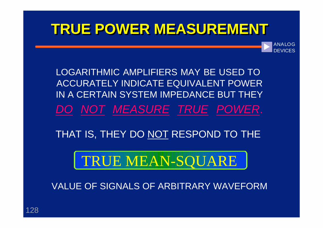
TRUE POWER MEASUREMENTTRUE POWER MEASUREMENT
LOGARITHMIC AMPLIFIERS MAY BE USED TO ACCURATELY INDICATE EQUIVALENT POWERIN A CERTAIN SYSTEM IMPEDANCE BUT THEY
DO NOT MEASURE TRUE POWER.
THAT IS, THEY DO NOT RESPOND TO THE
TRUE MEAN-SQUARE
VALUE OF SIGNALS OF ARBITRARY WAVEFORM

129
A N A LO GDEVICES
A COMPLEX RF SIGNAL
Q: What is the true power?
TRUE POWER MEASUREMENT

130
A N A LO GDEVICES
THE ACCURATE MEASUREMENT OF THE
ROOT-MEAN-SQUARE (RMS)
VALUE OF SIGNAL OF ARBITRARY WAVEFORMCAN BE ACHIEVED IN TWO WAYS:
k THERMAL DETECTORS k ANALOG COMPUTATION
TRUE POWER MEASUREMENT

131
A N A LO GDEVICES
k THERMAL DETECTORS
l Fundamentally correct l Very slow - milliseconds l Small dynamic range l Difficult to integrate
- need MEM structures
TRUE POWER MEASUREMENT

132
A N A LO GDEVICES
k ANALOG COMPUTATION
l Very accurate with good design l Can have large dynamic range
- 30dB for direct squaring
- up to 100dB using new methods
l Output can be linear-in-dB l Low Voltage and Power (<10mW)
- with chip enable
TRUE POWER MEASUREMENT

133
A N A LO GDEVICES
A BASIC METHODA BASIC METHOD
x 2
WIDE-BAND SQUARE-LAWTRANSCONDUCTANCECELL (BJT TECHNIQUES)
VIN
IO (VIN /VR )2
Intermediate current
RO
VOUT =
VIN
VO
AVE2
where
VO = VR2/IO RO
CO
This simple structure produces the Mean-Square of VIN
with an averaging time determined by the product CO RO
RF INPUT

134
A N A LO GDEVICES
A BASIC METHOD
l Very simple cell designl Can fit into a 1.5V supplyl Wideband -- to >6GHz
k ADVANTAGES
l Low dynamic range capacityl Higher dynamic range of outputl Complicated scaling mechanisms
k DISADVANTAGES

135
A N A LO GDEVICES
DIFFERENCE-OF-SQUARESDIFFERENCE-OF-SQUARES
VOUT =
VIN AVE2
Directly produces the Root-Mean-Square of VIN with an averaging time determined by the product CO RO
x 2 VIN
IO (VIN /VR )2
CORO
x 2
VOUT
IO (VOUT /VR )2
RO
+
-IDENTICALSQUARINGCIRCUITS
High-gain amplifier
RF INPUT
136
A N A LO GDEVICES
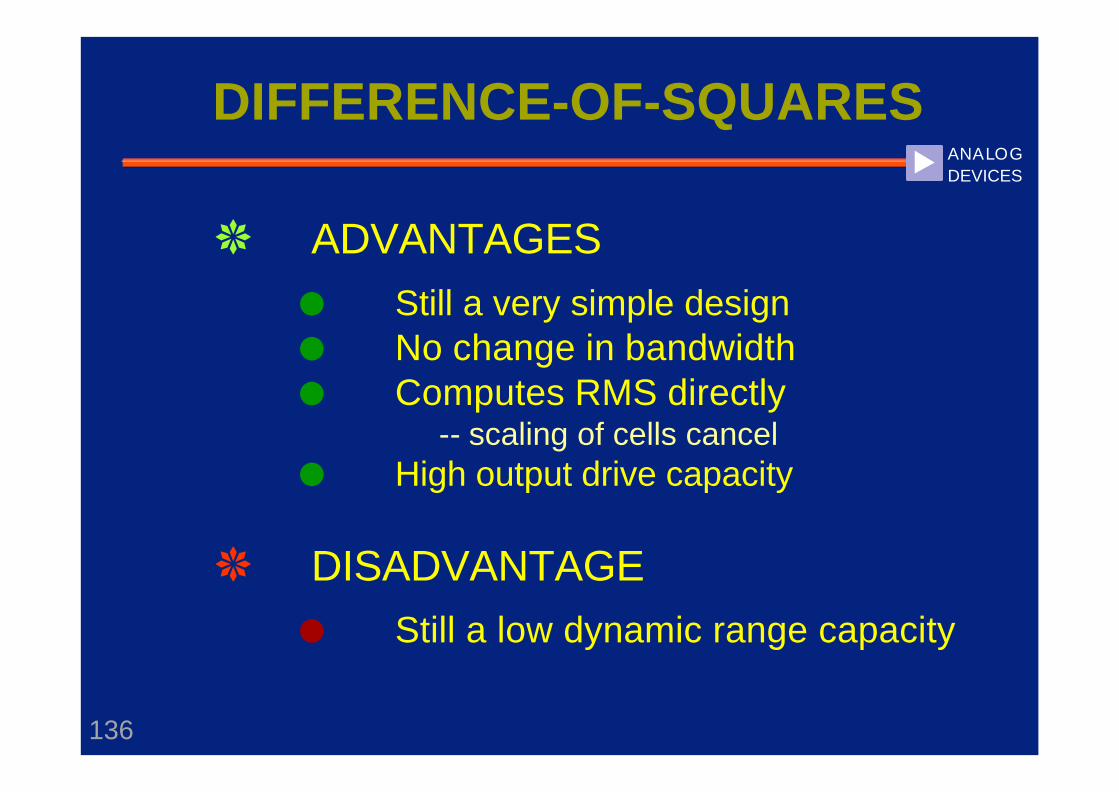
l Still a very simple designl No change in bandwidthl Computes RMS directly
-- scaling of cells cancell High output drive capacity
k ADVANTAGES
l Still a low dynamic range capacity
k DISADVANTAGE
DIFFERENCE-OF-SQUARES

137
A N A LO GDEVICES
l Uses a different squaring cell designl About the same bandwidth (>3GHz)
-- limited mostly by packagel Basically unlimited signal range
-- due to Class AB operationl Precisely-defined input impedancel Can provide over 30dB dynamic rangel Only 6mW quiescent consumption
k A COMPLETE IC POWER DETECTOR
AD8361AD8361

VIN
80dB Log-RMS Voltmeter80dB Log-RMS Voltmeter
AD8361VRMS
COMM
VPOS
PWDN
FLTR
RFIN
IREF
SREF
+5V+1XAMP
+5V
XAMP
Each VGA section is 1/2 AD605; theop amps are 1/2 AD8032; all operate from +5V; a single 2.5V reference (notshown) sets slope VY & intercept VZ.A few components omitted for clarity.
100Ω 100Ω2nF
220pF
220Ω
1µF
+5V
∞ +
Set-point,~1.2V
15kΩ
1µF
1nF
VOUT20mV/dB
3-pole low-pass, with corner at 2MHz
∆=40dB ∆=40dB
VOUT = VY log (VIN / VZ )
20µV -200mV rms
Variable-gain amplifier, 0-80dB
A N A LO GDEVICES

139
A NetworkAnalyzeron a Chip

140
w A Network Analyzer on a Chip! - Almost!
VGAIN = VG log (VA/VB ) VG = 30mV/dB
VPHS = VP ( φ 1 - φ 2 ) VP = 10mV/deg
w Operates from LF to >3 GHz
Applications– Power Amplifier Phase/Gain Control
.... independent of actual power level
– Monitoring of System Gain/Loss (e.g. Return Loss)– System Diagnostics– Linear Phase Demodulator
GAIN-PHASE DETECTORGAIN-PHASE DETECTORA N A LO GDEVICES

141
TRUE GAIN MEASUREMENTTRUE GAIN MEASUREMENTA N A LO GDEVICES
VA
V1 = VY log ( VA / VX )
VB V2 = VY log ( VB / VX )
Σ VY log ( VA / VB )
+
-
By subtracting the output of the B-channel log-amp from that of the A-channel log-amp, the intercept VX is eliminated andthe resulting difference is a measure of the RATIO of VA / VB
LA
LB

142
CANCELS PACKAGE RESONANCESCANCELS PACKAGE RESONANCESA N A LO GDEVICES
VA
VB
= VY log
+
-
Both channels have the same HF resonances and other HFtransmission effects g(f), but these are canceled in taking thedifference which remains a measure of the RATIO of VA / VB
εA= VAg(f)
εB= VBg(f)
VA g(f)VB g(f)
= VY logVA
VB
VOUT = VY logεA
εB LA
LB
Σ

143
PHASE MEASUREMENT at 2.5GHzPHASE MEASUREMENT at 2.5GHzA N A LO GDEVICES
VA
V1 = VY log ( VA / VX )
VB V2 = VY log ( VB / VX )
VY log ( VA / VB )
+
-
Logarithmic amplifiers also provide very high gain and limitingaction: using a special type of analog multiplier between thelimiter outputs, phase measurements can be made at 3GHz
LA
LB
ΣPHASEOUTPUT

144
APPLICATIONSAPPLICATIONSA N A LO GDEVICES
In this case, a low-frequency carrier provides avery high calibration reference for the intercept
RF signal to be measured
Low-frequencyreference carrier
LA
Σ
+
-Φ
LB
log(A/B)

145
A N A LO GDEVICES
Modulated RF signal
Basebandmodulation
Here, the reference is provided by the basebandmodulation & system measures conversion gain
log(A/B)
LA
Σ
+
-Φ
LB
APPLICATIONSAPPLICATIONS
146
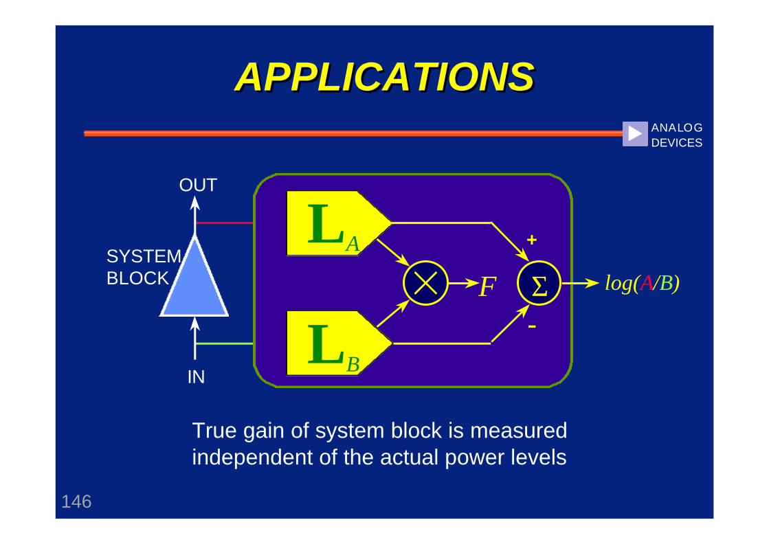
A N A LO GDEVICES
True gain of system block is measuredindependent of the actual power levels
log(A/B)
OUT
IN
SYSTEMBLOCK
LA
Σ
+
-Φ
LB
APPLICATIONSAPPLICATIONS

147
A N A LO GDEVICES
Measurement of return lossindependent of power level
log(A/B)
SOURCE
LOAD
CO
UP
LER
S LA
Σ
+
-Φ
LB
APPLICATIONSAPPLICATIONS

148
TheX-AMP

149
The X-AMP™The X-AMP™
l A PROPRIETARY VGA PRINCIPLE
l FUNDAMENTALLY “LINEAR-in-dB”
l USES FEEDBACK IN ORDER TO:
ACCURATELY DETERMINE GAIN
MINIMIZE HF NONLINEARITIES
l GUARANTEES ULTRA-LOW NOISE
l EXHIBITS WIDE DYNAMIC RANGE
FROM NOISE FLOOR (0.7µV RMS)
TO TYPICALLY 1.4V RMS (106dB)
A N A LO GDEVICES
150
X-AMP PRODUCTSX-AMP PRODUCTS
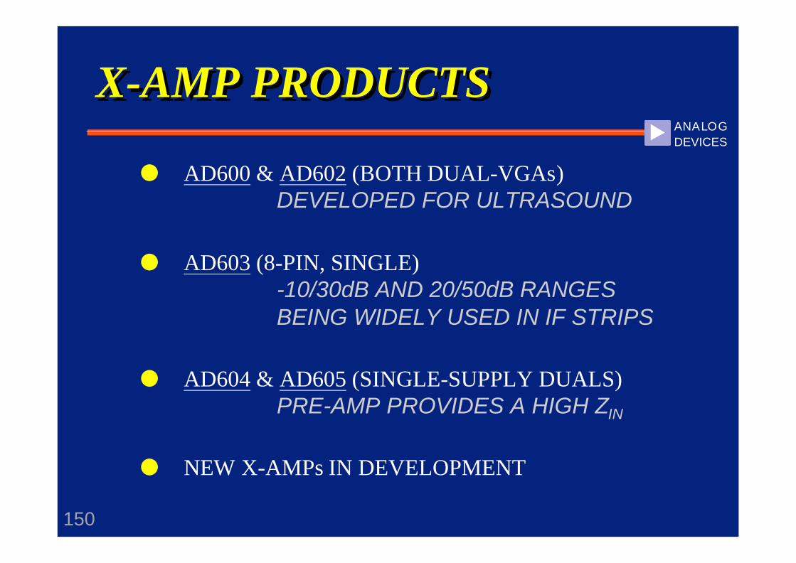
l AD600 & AD602 (BOTH DUAL-VGAs)DEVELOPED FOR ULTRASOUND
l AD603 (8-PIN, SINGLE)-10/30dB AND 20/50dB RANGESBEING WIDELY USED IN IF STRIPS
l AD604 & AD605 (SINGLE-SUPPLY DUALS)PRE-AMP PROVIDES A HIGH ZIN
l NEW X-AMPs IN DEVELOPMENT
A N A LO GDEVICES

151
THE BASIC X-AMPTHE BASIC X-AMP
R1R2R:nR ATTENUATOR
+
-VIN
VOUT
VARIABLE “SLIDER”
LOW-NOISEAMPLIFIER
RO
A N A LO GDEVICES

152
R2
VIN
VOUT
R
⌠ ⌠
gm1 gm2 gm7 gm8
R R
2R 2R R2R
0dB -6.02dB -36.12dB -42.14dB
VOUT - 41dB
R1200Ω 10
11*200Ω
iINTERPOLATING gm STAGES
TYPICAL 8-STAGE X-AMPTYPICAL 8-STAGE X-AMP
100Ω
A N A LO GDEVICES

153
gm1
CURRENTS IN THE gm STAGES
gm2 gm3 gm4 gm5 gm6 gm7gm8
INCREASING GAIN (MOVES ACTION TOWARDS FRONT) A N A LO G
DEVICES

154
MORE COMPLETE X-AMP MORE COMPLETE X-AMP
R1R2R:2R ATTENUATOR
VIN
VOUT
MAIN GAIN STAGE(acts as an integrator)
⌠⌠ GAUSSIAN INTERPOLATORVGAIN
20Ω
2.2kΩLASER-TRIMMEDFOR PRECISE GAIN
LASER-TRIMMEDFOR PRECISE RIN
LASER-TRIMMED FOR PRECISEGAIN - SCALING AND INTERCEPT
gm CELLS
A N A LO GDEVICES

SOLID-STATE POTENTIOMETERA N A LO GDEVICES
P-type region simultaneously serves as theNPN base, PMOS drain, and as a resistor
PMOS gate (poly-Si)N-type emitter
P-type region actsas PMOS source
(Contacts are shown in black)
N-typeburiedlayer
Collectorcontact (2)
Basecontact(2)

SOLID-STATE POTENTIOMETERA N A LO GDEVICES
Carrierdomain
Domain can be moved by voltage control from left to right
DOMAIN - CORRESPONDS TO ‘SLIDER’
C1 C2BURIED LAYER FORMS RESISTIVE TRACK

157
WhySiGe?

PLANAR NPNTRANSISTORPLANAR NPNTRANSISTOR
CE B
p substrate
p
iso
p
iso
n+ buried layer
n++
n+ emitter
SiO2 SiO2
n epitaxial layer
E B
p base
A N A LO GDEVICES

PLANAR NPNTRANSISTORPLANAR NPNTRANSISTOR
CE B
p
iso
p
iso
n+ buried layer
n++
n+ emitter
SiO2 SiO2
n epitaxial layer
E B
THIN BASE NEEDEDTO MINIMIZE TF ANDTHUS MINIMIZE QB FOR A GIVEN IC
p base
A N A LO GDEVICES

PLANAR NPNTRANSISTORPLANAR NPNTRANSISTOR
CE B
p
iso
p
iso
n+ buried layer
n++
n+ emitter
SiO2 SiO2
n epitaxial layer
E B
THIN BASE NEEDEDTO MINIMIZE TF ANDTHUS MINIMIZE QB FOR A GIVEN IC
BUT THIS RAISES RB,LOWERS VAF, LOWERSBVCEO AND CAN LEADTO COL-EM SHORTS
p base
A N A LO GDEVICES

PLANAR NPNTRANSISTORPLANAR NPNTRANSISTOR
CE B
p
iso
p
iso
n+ buried layer
n++
n+ emitter
SiO2 SiO2
n epitaxial layer
E B
THIN BASE NEEDEDTO MINIMIZE TF ANDTHUS MINIMIZE QB FOR A GIVEN IC
BUT THIS RAISES RB,LOWERS VAF, LOWERSBVCEO AND CAN LEADTO COL-EM SHORTS
POLY EMITTER RAISES EMITTER RESISTANCE RE
p base
A N A LO GDEVICES

162
l BEGIN BY USING AN EPITAXIALLY-GROWN BASEFILM RATHER THAN AN ION-IMPLANTED LAYER
l DURING BASE-FILM DEPOSITION ADD A SMALLPERCENTAGE OF GERMANIUM
l GRADE THE Ge CONCENTRATION; THIS WILLINTRODUCE A FIELD IN THE BASE
l ALSO, INCREASE THE CONCENTRATION OFTHE NORMAL BASE DOPANT (BORON)
KEY IDEAS ABOUT SiGeKEY IDEAS ABOUT SiGe
A N A LO GDEVICES

163
l A BASE FILM OF VERY PRECISELY CONTROLLEDCOMPOSITION, WITH A THICKNESS ACCURATETO WITHIN A FEW ATOMIC LAYERS
l A MUCH LOWER BASE RESISTANCE, DUE TO USEOF HIGHER BASE DOPING CONCENTRATION
l A MUCH HIGHER EARLY VOLTAGE, SINCE THEDEPLETION LAYER WIDTH IS SMALLER
l HIGH BETA IS ACHIEVED BECAUSE OF HIGHEREMITTER EFFICIENCY DUE TO REDUCTIONOF BAND-GAP ENERGY AT EMITTER EDGE
THIS BUYS YOU:THIS BUYS YOU:
A N A LO GDEVICES

164
l SUPER-ACCURATE BASE-WIDTH OF ABOUT0.1µm MEANS THAT TRANSIT TIME IS VERYSMALL AND VERY WELL CONTROLLED
l LOW BASE RESISTANCE ALSO INCREASESSPEED AND LOWERS JOHNSON NOISE
l HIGH EARLY VOLTAGE RAISES AVAILABLEGAIN & LOWERS COLLECTOR DISTORTION
l HIGH DC BETA SIMPLIFIES BIASING
TRANSLATED:TRANSLATED:
A N A LO GDEVICES

165
SIMILARITY TO A GaAs MESFET?SIMILARITY TO A GaAs MESFET?
THEY ARE BOTH VERY FAST SEMICONDUCTOR DEVICES
but
A SiGe HBT USES STANDARD SILICON WAFERS
IT DOES NOT HAVE ANY STRANGE SUBSTRATE EFFECTS (e.g. SLOW STATES) THAT PLAGUE GaAs
IT CAN BE INTEGRATED INTO VLSI USING BiCMOS
A N A LO GDEVICES

166
IN SHORT....IN SHORT....
THE BENEFITS OF SiGe, THOUGH MODEST, ARE REALENOUGH TO GUARANTEE WIDESPREAD ADOPTION INSTATE-OF-THE-ART IC PROCESS TECHNOLOGIES.
THE COMBINATION OF A 50GHz HBT WITH A 0.25µmCMOS PROCESS WILL BECOME STANDARD FOR USEIN MIXED-SIGNAL RF & IF SIGNAL-PROCESSING ICs.IN THESE PRODUCTS, WAFER COST IS NOT CRITICAL.
THIS PROCESS WILL BE VERY DURABLE, AND WILL NOT READILY BE OBSOLETED IN THIS PARTICULARCLASS OF APPLICATIONS FOR MANY YEARS.
A N A LO GDEVICES

167
What’sAhead?

168
The challenges facing designers of analog radio systems, now inextricably interwoven with the integrated circuit and the exclusive use of digital modulation, are considerable.
The economics of the mass market affect every aspect of system development, and dictate the use of ultra-low-cost processes, assembly, and testing techniques.
The Newtonian nature of radio remains an inescapable factor in approaching design.
RADIO IN THE INFORMATION AGE RADIO IN THE INFORMATION AGE

169
A N A LO GDEVICES
k PARTNERSHIPS IN TECHNOLOGY
l ANALOG teaming with DIGITAL
l BIPOLAR teaming with CMOS
l SOC’s teaming with SOH’s
l CONTAINED PROPAGATION (e.g fiber)
teaming with BROADCAST MODES
FUTURE TRENDSFUTURE TRENDS

170
A N A LO GDEVICES
k GREATER INTERCONNECTIVITY
l Demand for access will increase
l Bandwidth will become more affordable
l Home networks will become commonl Many data links will be radio-based, and use both microwave and long-wavel Distinction between “TV” and “PC” presentation of images will disappearl Un-self-conscious use of facial images in day-to-day communicationsl Wearable computers and communications
FUTURE TRENDSFUTURE TRENDS

171
A N A LO GDEVICES
k NEW PARADIGMS for DESIGN
l The present approaches to the design of integrated circuits and systems must be supplanted by more efficient ones, as systems become more complex
l This will entail greater re-use of proven cells, and of less time for highly-specific customization
l Increased use of advanced hybrid assembly techniques will generate a demand for a new kind of IC designer
l Fundamental analog design principles must be restored to curricula and mixed-signal techniques emphasized
l Today’s IC designers increasingly need to diversify
l Need to focus more strongly on the crucial issue of Design for Manufacture
FUTURE TRENDSFUTURE TRENDS

172
A N A LO GDEVICES
k INCREASING ELECTRONICS IN MEDICINE
l Already used in many investigative and diagnostic tools
l Small swallowable radio pills can report on temperature,
digestive chemistry, pressure, etc. Cheap transponders
can be given to a patient to connect to a PC or PDA
l An increasing use of prosthetic devices can be foreseen,
some of which may rely on ultra-short-range radio links
l Further advances in affordable ultra-fast computers will
facilitate the modeling of molecules and the development
of more effective disease-specific drugs
FUTURE TRENDSFUTURE TRENDS

173
A N A LO GDEVICES
k INCREASING DEPENDENCE ON GPS
l GPS is already finding a host of unexpected uses: in Paris,
buses are equipped; in Amsterdam, Berlin and Singapore,
taxi-cab are tracked by GPS; as are trucks in the USA:
farmers guide their tractors and other equipment by GPS
l Next step: universal use in automobiles, and other personal
transportation systems; these have numerous applications
l Wrist-watch GPS facilitates the location of key personnel
l Later: fully automated, GPS-guided transport systems
(Knowing the “where” will be as important knowing the “time”)
FUTURE TRENDSFUTURE TRENDS

174
A N A LO GDEVICES
k NEW PARADIGMS FOR COMPUTING?
l When will neural networks provide useful adjuncts
to serial, algorithmic machines? Perhaps by 2015
l Still at the fringes of practical utilization, quantum
computers approach problem solving in an entirely
novel manner, stressing the holistic physical aspects
of a system model, again in contrast to a reliance on
binary representations and serial algorithms
l Employing nuclear magnetic resonance (NMR) to
excite and then “listen to” molecular signatures, the
need for RF transceiver techniques is central
FUTURE TRENDSFUTURE TRENDS

175
SUMMARY
l ANALOG IS NOT OBSOLETE !l DESIGN CHALLENGES ABOUND
l BIPOLAR REMAINS IMPORTANT
l SYSTEM-on-a-HEADER may be a
good alternative to SoC VLSI
SUMMARY
l ANALOG IS NOT OBSOLETE !l DESIGN CHALLENGES ABOUND
l BIPOLAR REMAINS IMPORTANT
l SYSTEM-on-a-HEADER may be a
good alternative to SoC VLSI
exp
A N A LO GDEVICES