mic5304ww1.microchip.com/downloads/en/devicedoc/mic5304.pdfmicrel, inc. mic5304 november 2008 2...
TRANSCRIPT
MIC5304 Single 150mA Low Operating Current
LDO with Dual Voltage Pin Select
MLF and MicroLeadFrame are registered trademarks of Amkor Technology, Inc. Micrel Inc. • 2180 Fortune Drive • San Jose, CA 95131 • USA • tel +1 (408) 944-0800 • fax + 1 (408) 474-1000 • http://www.micrel.com
November 2008 M9999-111908-A
General Description The MIC5304 is a low quiescent current, low dropout regulator with selectable output voltage designed for applications that require two levels of output voltage regulation. The MIC5304 is an ideal solution for programming memory cards as well as for conserving power in portable applications. The MIC5304 is capable of sourcing 150mA of output current while only consuming 24µA of operating current. This high performance LDO offers fast transient response while still maintaining low quiescent current levels. The MIC5304 is an ideal solution for battery operated applications due to ultra low operating current and extremely low dropout voltage of 85mV at 150mA. Equipped with a TTL logic compatible enable pin, the MIC5304 can be put into a zero-off mode current state, drawing virtually no current when disabled. Board space and component cost is minimized because the MIC5304 operates with very small 1μF ceramic capacitors. The MIC5304 provides fixed output voltages, and is available in the tiny 1.6mm x 1.6mm Thin MLF® package ideal for portable electronics. MIC5304 also features thermal shutdown and current limit protection. Data sheets and support documentation can be found on Micrel’s web site at: www.micrel.com.
Features
• 150mA output current • Logic controlled selectable output voltage • Fast transition time between selected output voltages • Input voltage range: 2.3V to 5.5V • Low 24µA operating current • Stable with 1μF ceramic capacitors • Low dropout voltage of 85mV @ 150mA • Thermal shutdown and current limit protection • Tiny 6-pin 1.6mm x 1.6mm Thin MLF® package Applications • Mobile phones, PDAs, PMPs, PNDs • Digital still and video cameras • Dual voltage levels for power saving mode • Portable electronics
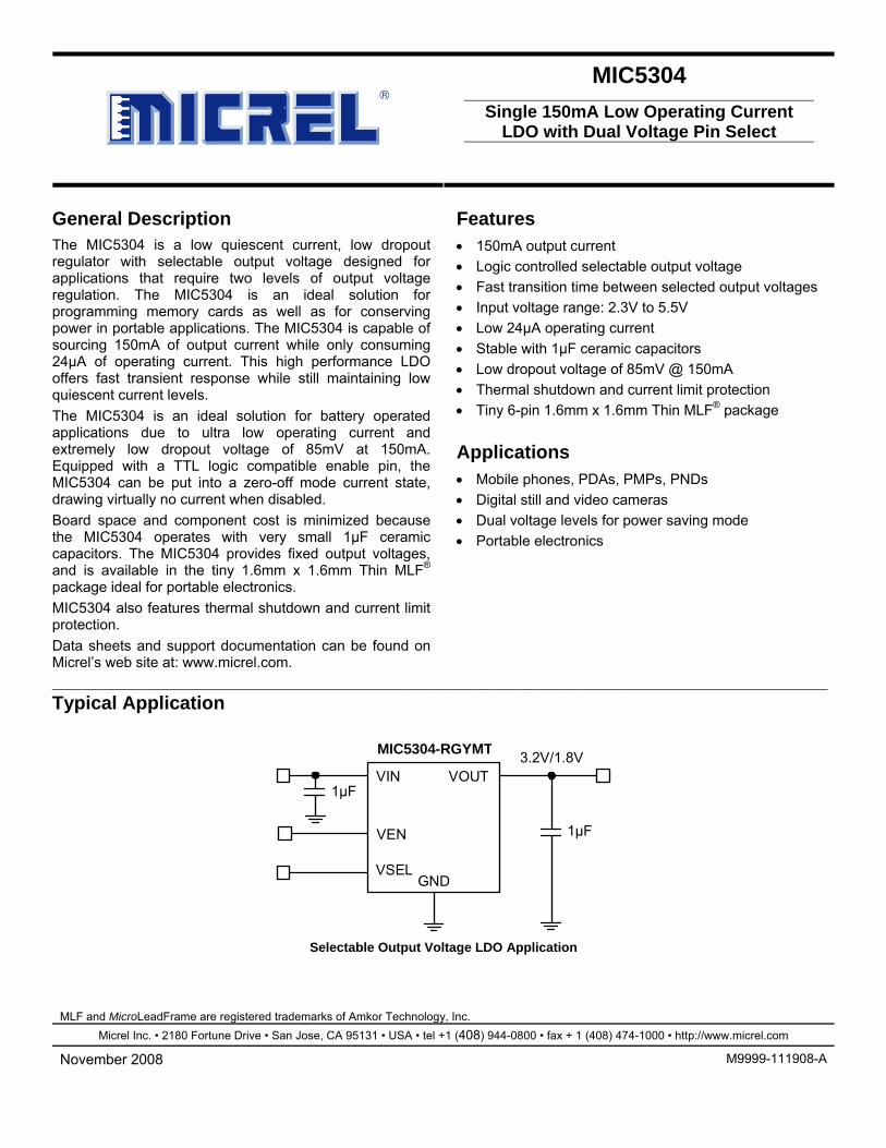
___________________________________________________________________________________________________________ Typical Application
MIC5304-RGYMT
VIN
VEN
VSEL
1µF
3.2V/1.8V
1µFVOUT
GND
Selectable Output Voltage LDO Application
Micrel, Inc. MIC5304
November 2008 2 M9999-111908-A
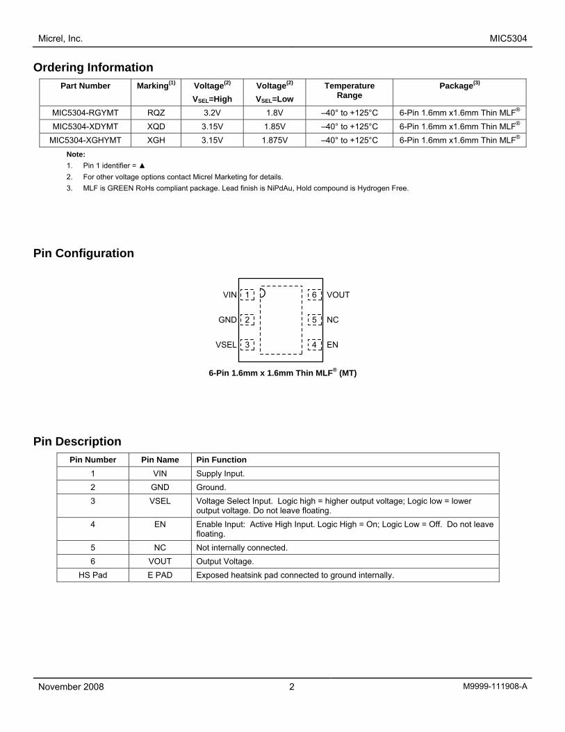
Ordering Information
Part Number Marking(1) Voltage(2) VSEL=High
Voltage(2) VSEL=Low
Temperature Range
Package(3)
MIC5304-RGYMT RQZ 3.2V 1.8V –40° to +125°C 6-Pin 1.6mm x1.6mm Thin MLF® MIC5304-XDYMT XQD 3.15V 1.85V –40° to +125°C 6-Pin 1.6mm x1.6mm Thin MLF®
MIC5304-XGHYMT XGH 3.15V 1.875V –40° to +125°C 6-Pin 1.6mm x1.6mm Thin MLF® Note:
1. Pin 1 identifier = 2. For other voltage options contact Micrel Marketing for details. 3. MLF is GREEN RoHs compliant package. Lead finish is NiPdAu, Hold compound is Hydrogen Free.
Pin Configuration
1VIN
GND
VSEL
6 VOUT
NC
EN
5
4
2
3
6-Pin 1.6mm x 1.6mm Thin MLF® (MT)
Pin Description Pin Number Pin Name Pin Function
1 VIN Supply Input. 2 GND Ground. 3 VSEL Voltage Select Input. Logic high = higher output voltage; Logic low = lower
output voltage. Do not leave floating. 4 EN Enable Input: Active High Input. Logic High = On; Logic Low = Off. Do not leave
floating. 5 NC Not internally connected. 6 VOUT Output Voltage.
HS Pad E PAD Exposed heatsink pad connected to ground internally.
Micrel, Inc. MIC5304
November 2008 3 M9999-111908-A
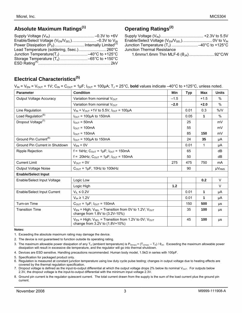
Absolute Maximum Ratings(1)
Supply Voltage (VIN) ........................................ –0.3V to +6V Enable/Select Voltage (VEN/VSEL). ..................... –0.3V to VIN Power Dissipation (PD) ........................... Internally Limited(3) Lead Temperature (soldering, 5sec.) ......................... 260°C Junction Temperature(TJ) .........................–40°C to +125°C Storage Temperature (Ts) .........................–65°C to +150°C ESD Rating(4).................................................................. 2kV
Operating Ratings(2)
Supply Voltage (VIN)....................................... +2.3V to 5.5V Enable/Select Voltage (VEN/VSEL)........................... 0V to VIN Junction Temperature (TJ) ........................–40°C to +125°C Junction Thermal Resistance 1.6mmx1.6mm Thin MLF-6 (θJA) .......................92°C/W
Electrical Characteristics(5) VIN = VEN = VOUT + 1V; CIN = COUT = 1µF; IOUT = 100µA; TJ = 25°C, bold values indicate –40°C to +125°C, unless noted.
Parameter Condition Min Typ Max Units Variation from nominal VOUT –1.5 +1.5 % Output Voltage Accuracy Variation from nominal VOUT –2.0 +2.0 %
Line Regulation VIN = VOUT +1V to 5.5V, IOUT = 100µA 0.01 0.3 %/V Load Regulation(6) IOUT = 100µA to 150mA 0.05 1 % Dropout Voltage(7) IOUT = 50mA
IOUT = 100mA IOUT = 150mA
25 55 85
150
mV mV mV
Ground Pin Current(8) IOUT = 100µA to 150mA 24 35 µA Ground Pin Current in Shutdown VEN = 0V 0.01 1 µA Ripple Rejection f = 1kHz; COUT = 1µF; IOUT = 150mA
f = 20kHz; COUT = 1µF; IOUT = 150mA 65
50 dB
dB Current Limit VOUT = 0V 275 475 750 mA Output Voltage Noise COUT = 1µF, 10Hz to 100kHz 90 µVRMS Enable/Select Input
Logic Low 0.2 V Enable/Select Input Voltage Logic High 1.2 V VIL ≤ 0.2V 0.01 1 µA Enable/Select Input Current VIH ≥ 1.2V 0.01 1 µA
Turn-on Time COUT = 1µF; IOUT = 150mA 150 500 µs VEN = High; VSEL = Transition from 0V to 1.2V; VOUT change from 1.8V to (3.2V-10%)
35 100 µs Transition Time
VEN = High; VSEL = Transition from 1.2V to 0V; VOUT change from 3.2V to (1.8V+10%)
45 100 µs
Notes: 1. Exceeding the absolute maximum rating may damage the device. 2. The device is not guaranteed to function outside its operating rating. 3. The maximum allowable power dissipation of any TA (ambient temperature) is PD(max) = (TJ(max) – TA) / θJA. Exceeding the maximum allowable power dissipation will result in excessive die temperature, and the regulator will go into thermal shutdown. 4. Devices are ESD sensitive. Handling precautions recommended. Human body model, 1.5kΩ in series with 100pF. 5. Specification for packaged product only. 6. Regulation is measured at constant junction temperature using low duty cycle pulse testing; changes in output voltage due to heating effects are covered by the thermal regulation specification. 7. Dropout voltage is defined as the input-to-output differential at which the output voltage drops 2% below its nominal VOUT. For outputs below 2.3V, the dropout voltage is the input-to-output differential with the minimum input voltage 2.3V. 8. Ground pin current is the regulator quiescent current. The total current drawn from the supply is the sum of the load current plus the ground pin current.
Micrel, Inc. MIC5304
November 2008 4 M9999-111908-A
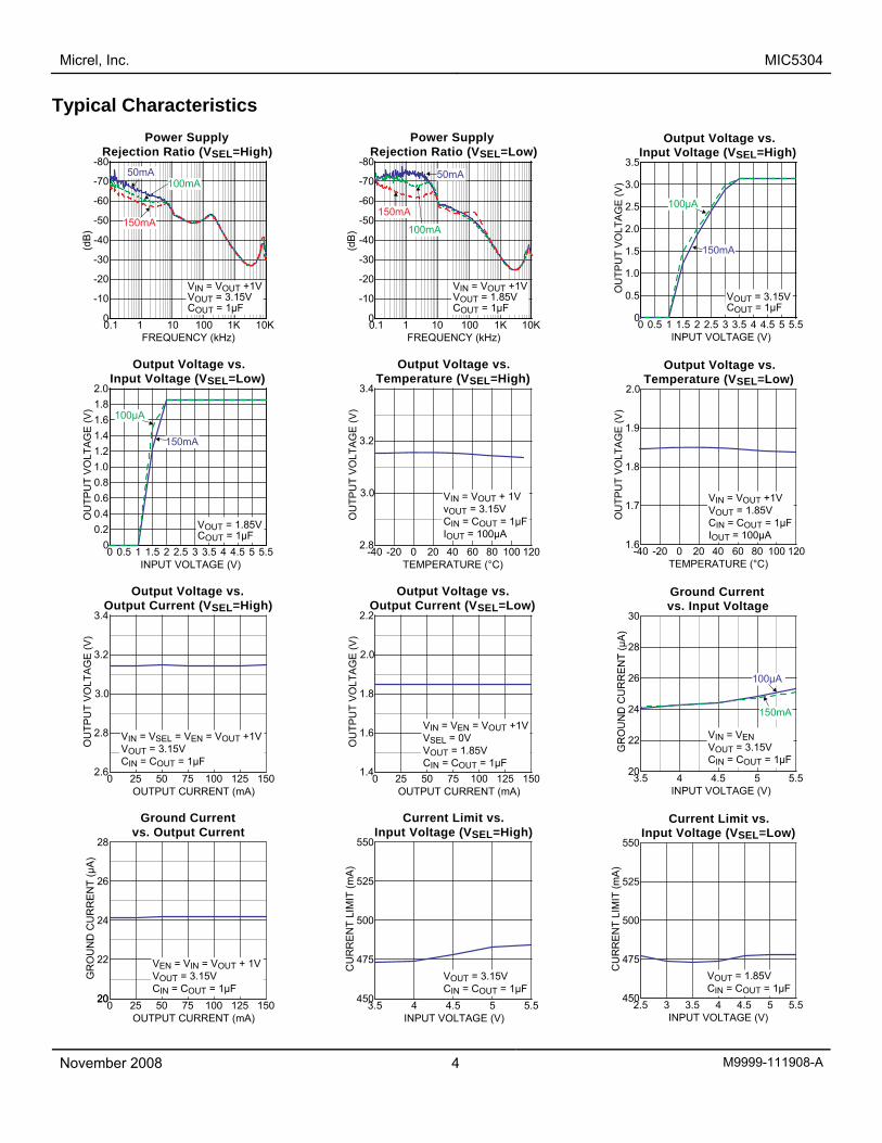
Typical Characteristics
0
-10
-20
-30
-40
-50
-60
-70
-80
Power SupplyRejection Ratio (VSEL=High)
1FREQUENCY (kHz)
0.1 10 100 1K
VIN = VOUT +1VVOUT = 3.15VCOUT = 1µF
100mA50mA
150mA
10K
0
-10
-20
-30
-40
-50
-60
-70
-80
Power SupplyRejection Ratio (VSEL=Low)
1FREQUENCY (kHz)
0.1 10 100 10K
VIN = VOUT +1VVOUT = 1.85VCOUT = 1µF
100mA
50mA
150mA
1K
0
0.5
1.0
1.5
2.0
2.5
3.0
3.5
0 0.5 1 1.5 2 2.5 3 3.5 4 4.5 5 5.5INPUT VOLTAGE (V)
Output Voltage vs.Input Voltage (VSEL=High)
100µA
150mA
VOUT = 3.15VCOUT = 1µF
00.20.40.60.8
1.21.41.61.8
0 0.5 1 1.5 2 2.5 3 3.5 4 4.5 5 5.5INPUT VOLTAGE (V)
1.0
2.0
Output Voltage vs.Input Voltage (VSEL=Low)
100µA
150mA
VOUT = 1.85VCOUT = 1µF
2.8
3.0
3.2
3.4
Output Voltage vs.Temperature (VSEL=High)
-40 -20 0 20 40 60 80 100 120TEMPERATURE (°C)
VIN = VOUT + 1VvOUT = 3.15VCIN = COUT = 1µFIOUT = 100µA
1.6
1.7
1.8
1.9
2.0
Output Voltage vs.Temperature (VSEL=Low)
-40 -20 0 20 40 60 80 100 120TEMPERATURE (°C)
VIN = VOUT +1VVOUT = 1.85VCIN = COUT = 1µFIOUT = 100µA
2.6
2.8
3.0
3.2
3.4
0 25 50 75 100 125 150OUTPUT CURRENT (mA)
Output Voltage vs.Output Current (VSEL=High)
VIN = VSEL = VEN = VOUT +1VVOUT = 3.15VCIN = COUT = 1µF
1.4
1.6
1.8
2.0
2.2
0 25 50 75 100 125 150OUTPUT CURRENT (mA)
Output Voltage vs.Output Current (VSEL=Low)
VIN = VEN = VOUT +1VVSEL = 0VVOUT = 1.85VCIN = COUT = 1µF
20
22
24
26
28
30
3.5 4 4.5 5 5.5INPUT VOLTAGE (V)
Ground Currentvs. Input Voltage
100µA
150mA
VIN = VENVOUT = 3.15VCIN = COUT = 1µF
20
22
24
26
28
0 25 50 75 100 125 150OUTPUT CURRENT (mA)
20
Ground Currentvs. Output Current
VEN = VIN = VOUT + 1VVOUT = 3.15VCIN = COUT = 1µF
450
475
500
525
550
3.5 4 4.5 5 5.5INPUT VOLTAGE (V)
Current Limit vs.Input Voltage (VSEL=High)
VOUT = 3.15VCIN = COUT = 1µF
450
475
500
525
550
2.5 3 3.5 4 4.5 5 5.5INPUT VOLTAGE (V)
Current Limit vs.Input Voltage (VSEL=Low)
VOUT = 1.85VCIN = COUT = 1µF
Micrel, Inc. MIC5304
November 2008 5 M9999-111908-A
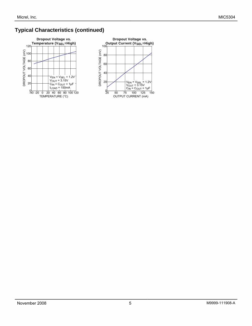
Typical Characteristics (continued)
0
20
40
60
80
100
120
Dropout Voltage vs.Temperature (VSEL=High)
-40 -20 0 20 40 60 80 100 120TEMPERATURE (°C)
VEN = VSEL = 1.2VVOUT = 3.15VCIN = COUT = 1µFILOAD = 150mA
0
20
40
60
80
100
25 50 75 100 125 150OUTPUT CURRENT (mA)
Dropout Voltage vs.Output Current (VSEL=High)
VEN = VSEL = 1.2VVOUT = 3.15VCIN = COUT = 1µF
Micrel, Inc. MIC5304
November 2008 6 M9999-111908-A
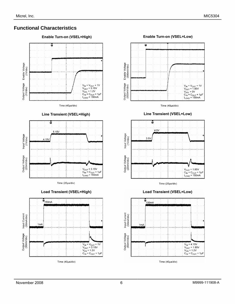
Functional Characteristics
Micrel, Inc. MIC5304
November 2008 7 M9999-111908-A
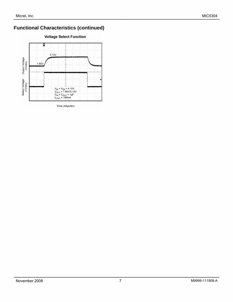
Functional Characteristics (continued)
Micrel, Inc. MIC5304
November 2008 8 M9999-111908-A
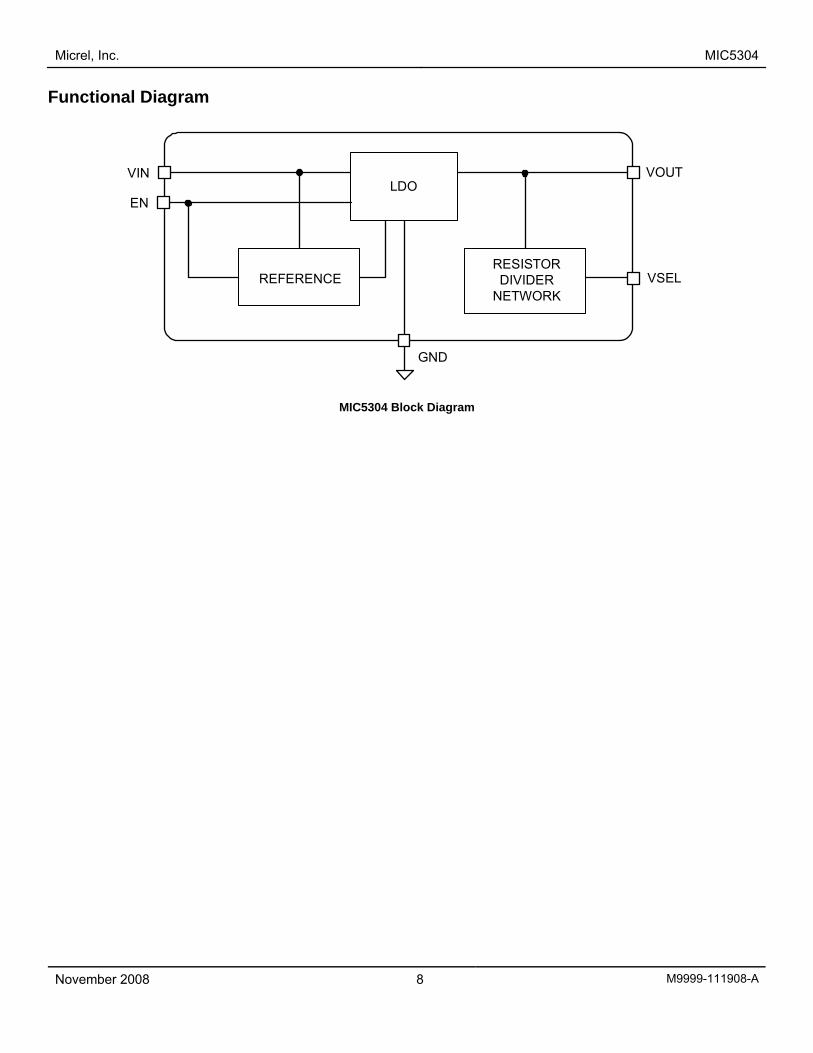
Functional Diagram
VIN
EN
GND
VOUT
VSEL
LDO
RESISTORDIVIDER
NETWORKREFERENCE
MIC5304 Block Diagram
Micrel, Inc. MIC5304
November 2008 9 M9999-111908-A
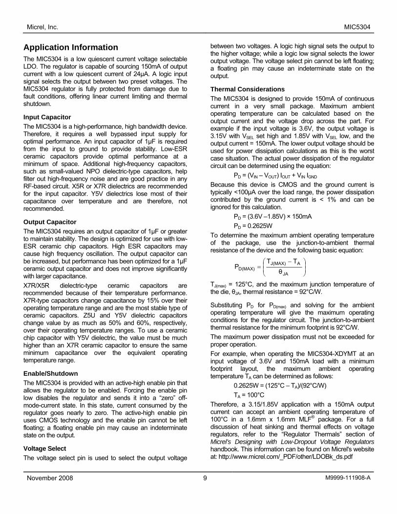
Application Information The MIC5304 is a low quiescent current voltage selectable LDO. The regulator is capable of sourcing 150mA of output current with a low quiescent current of 24µA. A logic input signal selects the output between two preset voltages. The MIC5304 regulator is fully protected from damage due to fault conditions, offering linear current limiting and thermal shutdown.
Input Capacitor The MIC5304 is a high-performance, high bandwidth device. Therefore, it requires a well bypassed input supply for optimal performance. An input capacitor of 1µF is required from the input to ground to provide stability. Low-ESR ceramic capacitors provide optimal performance at a minimum of space. Additional high-frequency capacitors, such as small-valued NPO dielectric-type capacitors, help filter out high-frequency noise and are good practice in any RF-based circuit. X5R or X7R dielectrics are recommended for the input capacitor. Y5V dielectrics lose most of their capacitance over temperature and are therefore, not recommended.
Output Capacitor The MIC5304 requires an output capacitor of 1µF or greater to maintain stability. The design is optimized for use with low-ESR ceramic chip capacitors. High ESR capacitors may cause high frequency oscillation. The output capacitor can be increased, but performance has been optimized for a 1µF ceramic output capacitor and does not improve significantly with larger capacitance. X7R/X5R dielectric-type ceramic capacitors are recommended because of their temperature performance. X7R-type capacitors change capacitance by 15% over their operating temperature range and are the most stable type of ceramic capacitors. Z5U and Y5V dielectric capacitors change value by as much as 50% and 60%, respectively, over their operating temperature ranges. To use a ceramic chip capacitor with Y5V dielectric, the value must be much higher than an X7R ceramic capacitor to ensure the same minimum capacitance over the equivalent operating temperature range.
Enable/Shutdown The MIC5304 is provided with an active-high enable pin that allows the regulator to be enabled. Forcing the enable pin low disables the regulator and sends it into a “zero” off-mode-current state. In this state, current consumed by the regulator goes nearly to zero. The active-high enable pin uses CMOS technology and the enable pin cannot be left floating; a floating enable pin may cause an indeterminate state on the output.
Voltage Select The voltage select pin is used to select the output voltage
between two voltages. A logic high signal sets the output to the higher voltage; while a logic low signal selects the lower output voltage. The voltage select pin cannot be left floating; a floating pin may cause an indeterminate state on the output.
Thermal Considerations The MIC5304 is designed to provide 150mA of continuous current in a very small package. Maximum ambient operating temperature can be calculated based on the output current and the voltage drop across the part. For example if the input voltage is 3.6V, the output voltage is 3.15V with VSEL set high and 1.85V with VSEL low, and the output current = 150mA. The lower output voltage should be used for power dissipation calculations as this is the worst case situation. The actual power dissipation of the regulator circuit can be determined using the equation: PD = (VIN – VOUT) IOUT + VIN IGND Because this device is CMOS and the ground current is typically <100µA over the load range, the power dissipation contributed by the ground current is < 1% and can be ignored for this calculation. PD = (3.6V –1.85V) × 150mA PD = 0.2625W To determine the maximum ambient operating temperature of the package, use the junction-to-ambient thermal resistance of the device and the following basic equation:
⎟⎟⎠
⎞⎜⎜⎝
⎛ −=
JA
AJ(MAX)D(MAX) θ
TTP
TJ(max) = 125°C, and the maximum junction temperature of the die, θJA, thermal resistance = 92°C/W.
Substituting PD for PD(max) and solving for the ambient operating temperature will give the maximum operating conditions for the regulator circuit. The junction-to-ambient thermal resistance for the minimum footprint is 92°C/W. The maximum power dissipation must not be exceeded for proper operation. For example, when operating the MIC5304-XDYMT at an input voltage of 3.6V and 150mA load with a minimum footprint layout, the maximum ambient operating temperature TA can be determined as follows: 0.2625W = (125°C – TA)/(92°C/W) TA = 100°C Therefore, a 3.15/1.85V application with a 150mA output current can accept an ambient operating temperature of 100°C in a 1.6mm x 1.6mm MLF® package. For a full discussion of heat sinking and thermal effects on voltage regulators, refer to the “Regulator Thermals” section of Micrel’s Designing with Low-Dropout Voltage Regulators handbook. This information can be found on Micrel's website at: http://www.micrel.com/_PDF/other/LDOBk_ds.pdf
Micrel, Inc. MIC5304
November 2008 10 M9999-111908-A
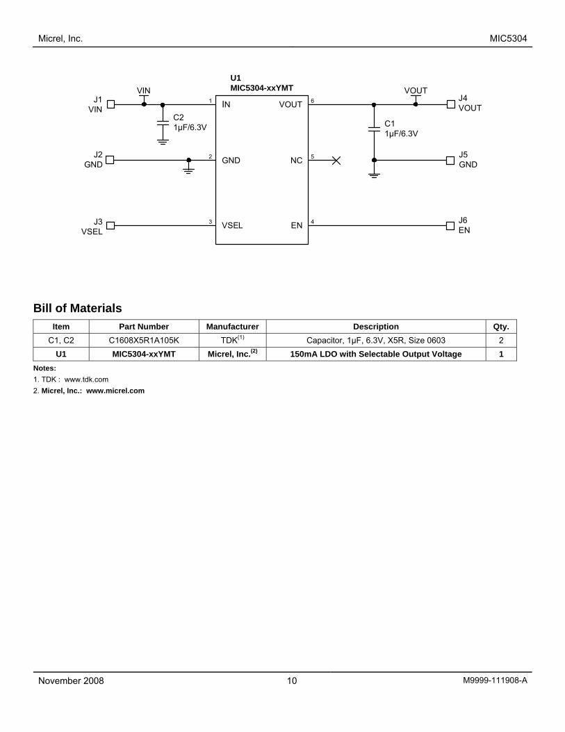
VIN VOUTJ4VOUTIN1
GND2
VSEL3
VOUT 6
EN 4
NC 5
U1MIC5304-xxYMT
J5GND
J6EN
C11µF/6.3V
J1VIN
J2GND
J3VSEL
C21µF/6.3V
Bill of Materials
Item Part Number Manufacturer Description Qty. C1, C2 C1608X5R1A105K TDK(1) Capacitor, 1µF, 6.3V, X5R, Size 0603 2
U1 MIC5304-xxYMT Micrel, Inc.(2) 150mA LDO with Selectable Output Voltage 1 Notes: 1. TDK : www.tdk.com 2. Micrel, Inc.: www.micrel.com

Micrel, Inc. MIC5304
November 2008 11 M9999-111908-A
PCB Layout Recommendations
Top Layer
Bottom Layer
Micrel, Inc. MIC5304
November 2008 12 M9999-111908-A
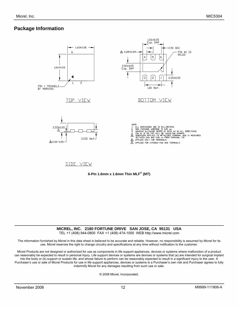
Package Information
6-Pin 1.6mm x 1.6mm Thin MLF® (MT)
MICREL, INC. 2180 FORTUNE DRIVE SAN JOSE, CA 95131 USA TEL +1 (408) 944-0800 FAX +1 (408) 474-1000 WEB http://www.micrel.com
The information furnished by Micrel in this data sheet is believed to be accurate and reliable. However, no responsibility is assumed by Micrel for its
use. Micrel reserves the right to change circuitry and specifications at any time without notification to the customer.
Micrel Products are not designed or authorized for use as components in life support appliances, devices or systems where malfunction of a product can reasonably be expected to result in personal injury. Life support devices or systems are devices or systems that (a) are intended for surgical implant
into the body or (b) support or sustain life, and whose failure to perform can be reasonably expected to result in a significant injury to the user. A Purchaser’s use or sale of Micrel Products for use in life support appliances, devices or systems is a Purchaser’s own risk and Purchaser agrees to fully
indemnify Micrel for any damages resulting from such use or sale.
© 2008 Micrel, Incorporated.