in the regular lab (science 208 - staff.tarleton.edu · in the regular lab (science 208) ... –all...
TRANSCRIPT
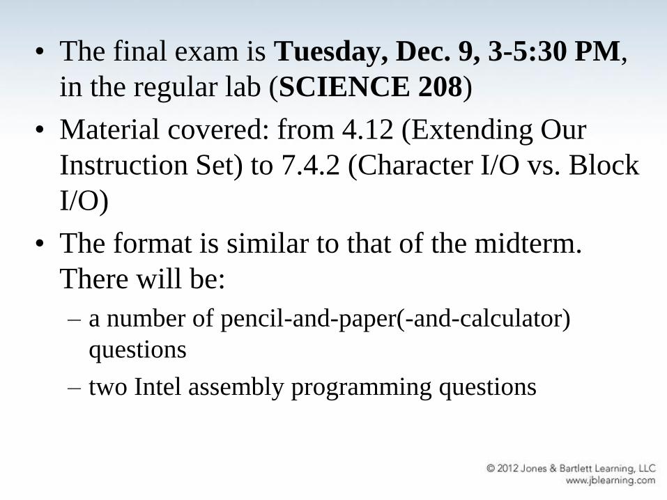
• The final exam is Tuesday, Dec. 9, 3-5:30 PM,
in the regular lab (SCIENCE 208)
• Material covered: from 4.12 (Extending Our
Instruction Set) to 7.4.2 (Character I/O vs. Block
I/O)
• The format is similar to that of the midterm.
There will be:
– a number of pencil-and-paper(-and-calculator)
questions
– two Intel assembly programming questions

How to study for the final:
• Read your notes and the instructor’s notes
(posted on our webpage at agapie.net)
• (Re)Solve:
– all in-class quizzes
– all homework problems
– all lab questions and assembly programming
exercises
• In addition to the above, the following questions
are provided:

In addition to the cheat-sheet (1 sheet, front
and back), you should have with you all the
text tables and figures provided by the
instructor as handouts in class.
Let the instructor know now if you need any
extra copies (or make your own from the
slides).
Do not mass-print the slides!

Chapter 4
MARIE: An Introduction
to a Simple Computer

In order to avoid confusion, there will
be no programming assignments in
MARIE assembly (only in Intel x86).
5

4.12 Extending our Instruction Set
6
7
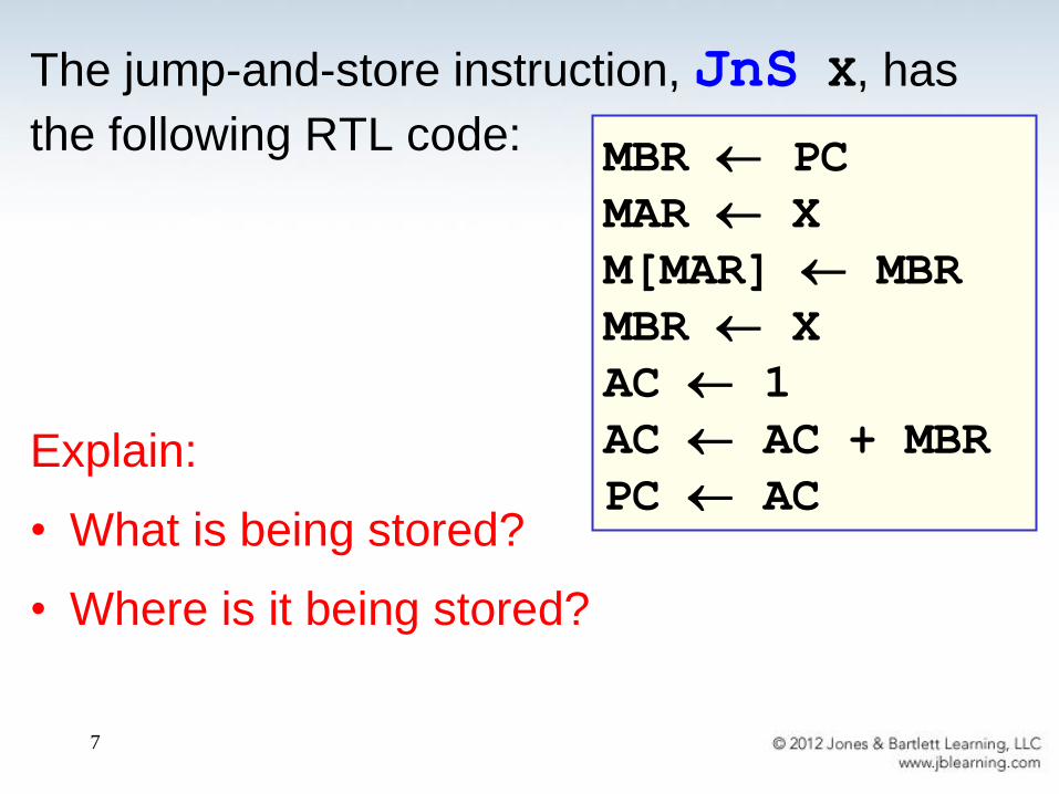
The jump-and-store instruction, JnS X, has
the following RTL code:
Explain:
• What is being stored?
• Where is it being stored?
MBR PC
MAR X
M[MAR] MBR
MBR X
AC 1
AC AC + MBR
PC AC

8
The jump-and-store instruction, JnS X, has
the following RTL code:
The Intel x86 instruction
that is similar in function to
JnS is __________ .
MBR PC
MAR X
M[MAR] MBR
MBR X
AC 1
AC AC + MBR
PC AC

List two differences between MARIE’s JnS
and Intel’s CALL:
9

List two differences between MARIE’s JnS
and Intel’s CALL:
• JnS X stores the return address at address X,
whereas CALL pushes it on the stack.
– MARIE does not have a stack!
• With JnS, the subroutine code starts at X+1,
whereas with CALL it starts at X.
10

11
Explain in a paragraph the concepts of:
• Hardwired decoding
• Microprogrammed decoding
4.13 Decoding

12
QUIZ Hardwired Decoding:
Based on the instruction opcodes, create the
decoder outputs for Output and Skipcond
13
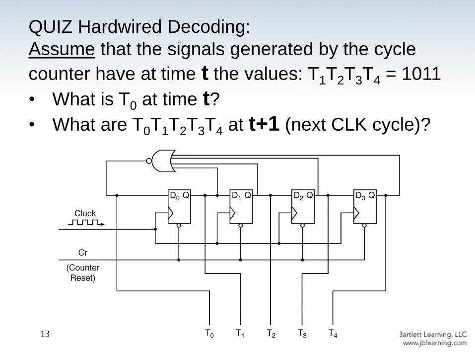
QUIZ Hardwired Decoding:
Assume that the signals generated by the cycle
counter have at time t the values: T1T2T3T4 = 1011
• What is T0 at time t?
• What are T0T1T2T3T4 at t+1 (next CLK cycle)?
14
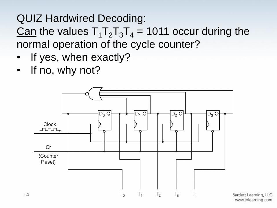
QUIZ Hardwired Decoding:
Can the values T1T2T3T4 = 1011 occur during the
normal operation of the cycle counter?
• If yes, when exactly?
• If no, why not?


16

17

18
When MicroOp2 is not 00000:
• MicroOp1 must be ______________________
• Jump must be __________________________
• Dest must be __________________________
Microprogrammed Decoding
Fill in the blanks:

19
• Does MicroOp2 really need to be 5 bits long? Explain,
either way.
• Does Dest really need to be 5 bits long? Explain, either way.
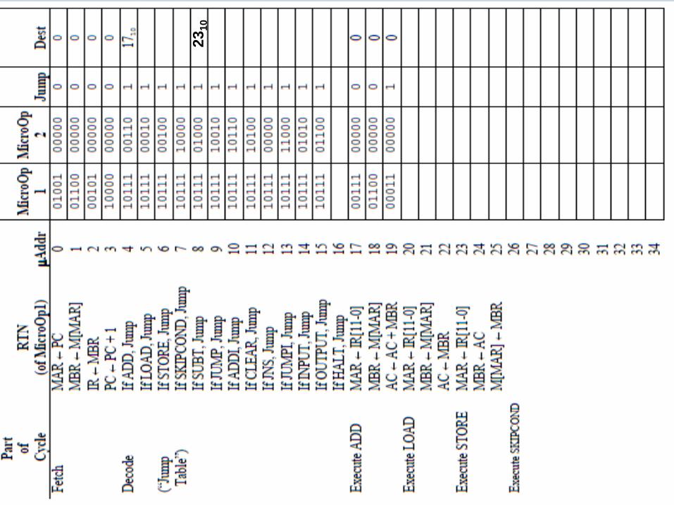
Microprogrammed Decoding:

Explain in detail the execution of the microprogram when
we execute instruction SUBT One from Example 4.1, by
filling out the corresponding part of the Control Store
(Microprogram Memory) shown below:
20
21
23
10

Chapter 5 A Closer Look at
Instruction Set Architectures

•23
Represent the hexadecimal number B1B2C3D4 in
big- and little-endian formats
QUIZ Endianness

•24
QUIZ Instruction Formats
• What are the three main choices for an ISA?
• Do all stack operations have zero operands?
• How would we implement LOAD and STORE in a
pure GPA architecture?
• A GPR ISA can have up to 4 operands, which can
be placed in one of 64 available registers. What is
the minimum instruction length?

•25
Stacks, postfix
Convert the infix expression,
Z = (X Y -1) + (W / U)
to postfix notation:

QUIZ: Is this a valid postfix expression?
1 2 3 4 + 5 6 - /
• If yes, what is the result?
• If no, why not?
•26

•27
Convert the expression
(3+7)/2∙(4+1)
to postfix and write a program to evaluate it in a zero-
address (stack) ISA.

•28
In a GPR ISA, there are 6 registers.
We need:
• 51 instructions with 3 operands
• 32 instr. with 2 operands
• 40 instr. with 1 operand
• 10 instr. with 0 operands
A. Find the minimum instruction length.
B. Design the instruction format using the length found above.

Explain in your own words how we find the
operand in each of these addressing modes:
•29

QUIZ: Addressing

31
QUIZ: Pipelining Speedup
n
Consider two different CPUs. The first is non-pipelined, with a
cycle time of 4ns. The second is pipelined, with four
pipeline stages and a cycle time of 1ns.
a. What is the speedup of the pipelined machine, assuming
no hazards and a large # of instructions?
b. What is the speedup of the pipelined machine versus the
single cycle machine if the pipeline stalls 1 cycle for 30% of
the instructions?

32
QUIZ: Pipelining Speedup
n
Consider two different CPUs. The first is non-pipelined, with a
cycle time of 4ns. The second is pipelined, with four
pipeline stages and a cycle time of 1ns.
c. Now consider a 3 stage pipeline machine with a cycle time
of 1.1ns. Again assuming many instructions and no stalls, is
this implementation faster or slower than the original 4 stage
pipeline? Explain.
QUIZ:


Chapter 6 Memory
•37
• cache hit
• cache miss
• hit rate
• miss rate
• hit time
• miss penalty
• DRAM
• SRAM
Explain in your own words:

•38
When an add for a computer says "6GB DDR3",
does it mean DRAM or SRAM? Explain.
Which is faster, DRAM or SRAM?
Which is cheaper?
What is memory refresh, when and why is it
needed?

•39
6.4 Cache Memory
Why is the cache always much smaller than the main
memory?
Name the 3 cache mapping algorithms we studied.
Name 2 of the 4 cache replacement policies we
studied.

•40
A byte-addressable memory uses 13 bits for
addresses.
The cache has 32 blocks, of size 4 Bytes each.
Show how the address is to be split into fields for
each of these caches:
• Direct-mapped
• Fully associative
• 8-way set-associative

•41
In each case, explain what the cache controller does when
the MM address 1BC7 is needed by the CPU.
A byte-addressable memory uses 13 bits for
addresses.
The cache has 32 blocks, of size 4 Bytes each.
Show how the address is to be split into fields for
each of these caches:
• Direct-mapped
• Fully associative
• 8-way set-associative

•42
A computer system has a MM access time of 150 ns
supported by a cache having a 5 ns access time.
The cache and MM accesses are non-overlapped.
We want the EAT to be 6 ns or under.
What is the minimum hit rate?
•43
A computer system has a MM access time of 150 ns
supported by a cache having a 5 ns access time.
The cache and MM accesses are non-overlapped.
We want the EAT to be 6 ns or under.
What is the minimum hit rate if the hardware allows
overlapped MM accesses?

•44
The cache has 3 sets, and it is initially empty.
The CPU is requesting the following sequence of blocks:
11, 1, 1, 2, 3, 42, 1, 2, 3, 4, 1, 2, 3
Show the state of the cache at the end of the
sequence:
QUIZ: LRU bit
Not in text, but required!

•45
11, 1, 1, 2, 3, 42, 1, 2, 3, 4, 1, 2, 3

•46
• write through
• write back
• The cache coherence problem
• Trace cache
• Victim cache
• Inclusive cache
• Exclusive cache
• L1, L2, L3 caches
• Harvard cache
• Unified cache
• Caching vs. paging
Explain in your own words:

How is paging different from segmentation?
How is internal fragmentation different from
external? Where does each occur?
QUIZ:

Chapter 7
Input/Output and
Storage Systems

•49
Amdahl’s Law: Exercise 8 at the and of Ch.7
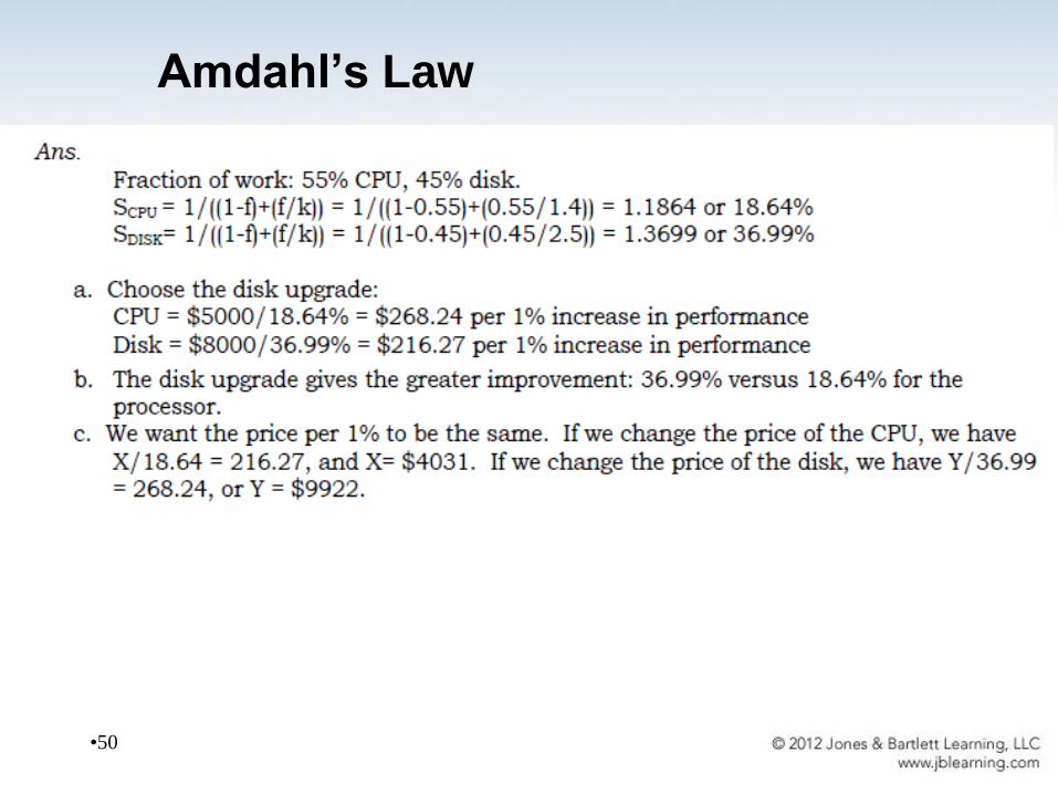
•50
Amdahl’s Law

•51
I/O can be controlled in five general ways:
• Programmed (a.k.a. polled) I/O reserves a register
for each I/O device. CPU continually polls these
registers (“new data” bit) to detect data arrival.
• Interrupt-Driven I/O allows the CPU to do other
things until I/O is requested.
• Memory-Mapped I/O shares memory address space
between I/O devices and program memory.
• Direct Memory Access (DMA) offloads I/O
processing to a special-purpose chip that takes care
of the details.
• Channel I/O uses dedicated I/O processors and a
separate I/O bus.
7.4 I/O Architectures

•52
Explain how and
why DMA “steals
cycles” from CPU.
DMA

•53
Explain the
difference between
“cycle-stealing” and
block-oriented
DMA operation.
DMA

54

55