implementing a cdc7005 low jitter clock - texas instruments
TRANSCRIPT

Application ReportSLWA034 - December 2004
1
Implementing a CDC7005 Low Jitter Clock Solution ForHigh-Speed, High-IF ADC Devices
Russell Hoppenstein / Firoj Kabir Wireless Infrastructure
ABSTRACT
Texas Instruments has introduced a family of devices suited to meet the demand forhigh-speed, high-IF sampling ADC devices like the ADS5500 ADC, capable of sampling at125 MSPS. To realize the full potential of these high performance devices, it is imperative toprovide an extremely low phase noise clock source. The CDC7005 clock distribution chipoffers a real-world clocking solution to meet the stringent requirements for high-speed ADCs.This report highlights the limiting agents associated with the clock source that adverselyaffect the ADC’s signal-to-noise performance. The performance of the ADS5500 ADCclocked with the CDC7005 is shown and compared to ideal baseline performance. Furtherimprovement topologies are presented along with measured results that show the CDC7005can meet or exceed the specifications at high sampling rates, even at the more demandinghigh input frequencies.
Contents
1 Introduction 3. . . . . . . . . . . . . . . . . . . . . . . . . . . . . . . . . . . . . . . . . . . . . . . . . . . . . . . . . . . . . . . . . . . . . . . . .
2 High IF Sampling Challenges 5. . . . . . . . . . . . . . . . . . . . . . . . . . . . . . . . . . . . . . . . . . . . . . . . . . . . . . . . .
3 Effect of Clock Amplitude 8. . . . . . . . . . . . . . . . . . . . . . . . . . . . . . . . . . . . . . . . . . . . . . . . . . . . . . . . . . . .
4 CDC7005 Clocking Solution 10. . . . . . . . . . . . . . . . . . . . . . . . . . . . . . . . . . . . . . . . . . . . . . . . . . . . . . . . .
5 CDC7005 Design Considerations 11. . . . . . . . . . . . . . . . . . . . . . . . . . . . . . . . . . . . . . . . . . . . . . . . . . . . 5.1 VCXO Requirement 11. . . . . . . . . . . . . . . . . . . . . . . . . . . . . . . . . . . . . . . . . . . . . . . . . . . . . . . . . . . . . . 5.2 Proper Terminations 12. . . . . . . . . . . . . . . . . . . . . . . . . . . . . . . . . . . . . . . . . . . . . . . . . . . . . . . . . . . . . 5.3 Layout Considerations 13. . . . . . . . . . . . . . . . . . . . . . . . . . . . . . . . . . . . . . . . . . . . . . . . . . . . . . . . . . .
6 CDC7005 Clock Source for the ADS5500 15. . . . . . . . . . . . . . . . . . . . . . . . . . . . . . . . . . . . . . . . . . . . .
7 Performance Improvements 18. . . . . . . . . . . . . . . . . . . . . . . . . . . . . . . . . . . . . . . . . . . . . . . . . . . . . . . . . 7.1 Improved Jitter 18. . . . . . . . . . . . . . . . . . . . . . . . . . . . . . . . . . . . . . . . . . . . . . . . . . . . . . . . . . . . . . . . . . 7.2 Lower Thermal Noise 19. . . . . . . . . . . . . . . . . . . . . . . . . . . . . . . . . . . . . . . . . . . . . . . . . . . . . . . . . . . .
8 Conclusion 23. . . . . . . . . . . . . . . . . . . . . . . . . . . . . . . . . . . . . . . . . . . . . . . . . . . . . . . . . . . . . . . . . . . . . . . . .
9 References 24. . . . . . . . . . . . . . . . . . . . . . . . . . . . . . . . . . . . . . . . . . . . . . . . . . . . . . . . . . . . . . . . . . . . . . . . .
Trademarks are the property of their respective owners.
SLWA034
2 Implementing a CDC7005 Low Jitter Clock Solution For High-Speed, High-IF ADC Devices
List of Figures
1 ADS5500 ADC With CDC7005 Clocking Solution Within A Typical Base Station Architecture 4. . . . . 2 SNR Degradation Due to Jitter for Different IF Input Signals 6. . . . . . . . . . . . . . . . . . . . . . . . . . . . . . . . . . 3 Measured vs Predicted SNR Performance Over Input Frequency 7. . . . . . . . . . . . . . . . . . . . . . . . . . . . . 4 Thermal Noise Component Causing Sampling Error 8. . . . . . . . . . . . . . . . . . . . . . . . . . . . . . . . . . . . . . . . 5 Thermal Noise Effect for Different Slope Clock Signals 9. . . . . . . . . . . . . . . . . . . . . . . . . . . . . . . . . . . . . . 6 Thermal Noise Effect for Different Amplitude Sinusoids 10. . . . . . . . . . . . . . . . . . . . . . . . . . . . . . . . . . . . . 7 VCXO to CDC7005 Interface 11. . . . . . . . . . . . . . . . . . . . . . . . . . . . . . . . . . . . . . . . . . . . . . . . . . . . . . . . . . . . 8 Phase Noise Measurement of the CDC−VCXO Compared With HP8644B 12. . . . . . . . . . . . . . . . . . . . 9 CDC7005 Terminations 13. . . . . . . . . . . . . . . . . . . . . . . . . . . . . . . . . . . . . . . . . . . . . . . . . . . . . . . . . . . . . . . . . 10 Grounding and Supply Connection Schemes for the CDC7005 14. . . . . . . . . . . . . . . . . . . . . . . . . . . . . . 11 Supply Bypassing for the CDC7005 15. . . . . . . . . . . . . . . . . . . . . . . . . . . . . . . . . . . . . . . . . . . . . . . . . . . . . 12 ADC Evaluation Test Set Up (Baseline) 15. . . . . . . . . . . . . . . . . . . . . . . . . . . . . . . . . . . . . . . . . . . . . . . . . . 13 ADC Evaluation Test Setup With the CDC7005 Clocking Source 16. . . . . . . . . . . . . . . . . . . . . . . . . . . . 14 SNR Performance vs IF Input Frequency 17. . . . . . . . . . . . . . . . . . . . . . . . . . . . . . . . . . . . . . . . . . . . . . . . 15 Spectral Performance With the CDC7005 Clock Source at 155-MHz IF Input 17. . . . . . . . . . . . . . . . . 16 Phase Noise Comparisons of CDC7005 Output With PECL and LVDS VCXOs 18. . . . . . . . . . . . . . . . 17 SNR Improvement With Lower Phase Noise VCXO Source 19. . . . . . . . . . . . . . . . . . . . . . . . . . . . . . . . . 18 Phase Noise of the CDC7005 With the Amp and BPF Compared to the Unmodified Output 20. . . . . 19 CDC7005 Clocking Topology With An Amplifier and Filter 21. . . . . . . . . . . . . . . . . . . . . . . . . . . . . . . . . . 20 SNR Response With Improved Clocking Topology 22. . . . . . . . . . . . . . . . . . . . . . . . . . . . . . . . . . . . . . . . . 21 Spectral Plot With CDC7005 Clock Plus Amplifier−BPF at 190-MHz IF Input 22. . . . . . . . . . . . . . . . . . 22 ADS5553 SNR Performance Over Input Frequency With New CDC7005 Clock Topology 23. . . . . . .
List of Tables
1 SNR and SFDR Measurements With the CDC7005 Clock 16. . . . . . . . . . . . . . . . . . . . . . . . . . . . . . . . . . 2 SNR and SFDR Comparisons With A Modified Clock Solution 21. . . . . . . . . . . . . . . . . . . . . . . . . . . . . . .
SLWA034
3 Implementing a CDC7005 Low Jitter Clock Solution For High-Speed, High-IF ADC Devices
1 Introduction
New transceiver architectures and PA linearization techniques are being investigated with theintroduction of high sampling rate and high IF capability analog-to-digital converters (ADCs). Forexample, digital predistortion requires high sampling rate ADCs to convert the output spectrumof the PA, including the desired signal and the third and fifth order intermodulation products, forlinearization processing. The bandwidth requirements for a multi-carrier WCDMA PA can be ashigh as 100 MHz. This requires high sampling rate ADCs to suitably capture the signal.
For new receiver designs with multi-carrier signals incorporating cost-savings topologies, thereis a need for high IF sampling ADCs. This effectively eliminates the need for a second analogmixer or analog demodulator which simplifies the receiver architecture. A high IF ADC isrequired to sample the signal at these frequencies with sufficient purity for the advancedtelecommunication standards.
Texas Instruments offers a series of high IF, high sampling rate ADCs suitable for the wirelessinfrastructure market. The ADS5500 is the industry leading 14-bit, 125-MSPS ADC that iscapable of achieving good SNR performance with high input frequency signals. In order torealize the devices’ full potential, it is important that the clock source have low phase noise. Thisrequirement is often overlooked when evaluating and designing with high-end ADCs. Further,though a suitable source may be used for evaluating purposes, finding a board level solutionoften proves difficult.
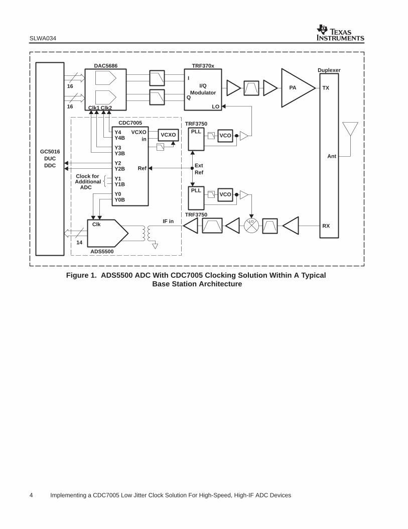
Texas Instruments introduces a board level, low phase noise clocking solution for the ADS5500and other high speed ADC devices using the CDC7005 clock distribution chip. With properconfiguration, the CDC7005 can be used with Texas Instruments high-speed ADCs to achieveideal performance that is suitable for direct implementation into PCB designs. In addition, theCDC7005 has the capability to drive five independent outputs that can be independently divideddown by 2n (n = 0 to 4). This allows one clock circuitry to provide a clock source for not only thehigh performance ADCs, but also the other devices on the board requiring an independent clocksuch as DACs (digital-to-analog converters), DDCs (digital down-converters), and DUCs (digitalup-converters). Figure 1 illustrates how the CDC7005 is utilized with the ADC and other devicesin a typical transceiver block diagram.
SLWA034
4 Implementing a CDC7005 Low Jitter Clock Solution For High-Speed, High-IF ADC Devices
TRF3750
Clock forAdditional
ADC
ADS5500
IF inClk
14
VCXO
Y0Y0B
Y1Y1B
Y2Y2B
Y3Y3B
Y4Y4B
Ref ExtRef
VCXOin
CDC7005
DAC5686
Clk1 Clk2
PA
TRF3750PLL
LO
TX
RX
Ant
VCO
LO
I
Q
TRF370x
I/QModulator
16
16
Duplexer
GC5016DUCDDC
PLL
VCO
Figure 1. ADS5500 ADC With CDC7005 Clocking Solution Within A Typical Base Station Architecture
SLWA034
5 Implementing a CDC7005 Low Jitter Clock Solution For High-Speed, High-IF ADC Devices
2 High IF Sampling Challenges
Clock jitter is defined as the random variation of the clock position compared to its ideal positionwith respect to time. When the position of the clock varies slightly, it alters the position of thesampling point which in turn samples the input waveform at an imprecise location. This errormanifests itself as a signal-to-noise (SNR) degradation.
The SNR degradation attributed to the jitter of the clock is defined as:
SNRj 20 log
Vfs2
2 fin 10 j
2
Vin20
Where:
Vfs = Full-scale voltage of the ADC
Vin = Relative input amplitude of the signal compared to Vfs expressed in dBFSfin = Input frequencytj = Clock jitter expressed in seconds
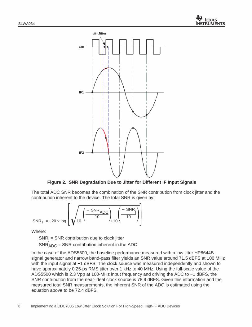
Note that the SNR degradation due to clock jitter is independent of the sampling rate; however, itis dependent on the input frequency. If it is noted that the expression inside the brackets is lessthan unity, then by increasing the input frequency the SNR contribution from the clock jitterbecomes more significant. In other words, for a given amount of clock jitter, a higher input IFsignal will be more susceptible to SNR degradation. This phenomenon is illustrated in Figure 2.Figure 2 depicts two IF input signals at different frequencies. An ideal clock source with a givenamount of jitter samples each signal. The ideal sampling point is shown at the dot, but the jitterwill alter the exact point where the signal is sampled. The potential points that could be sampledare depicted by the bold red line between the dashes. The error line on the lower frequencysignal is smaller than that on the higher frequency signal. As a result, the higher IF signal willhave higher SNR degradation due to clock jitter.
SLWA034
6 Implementing a CDC7005 Low Jitter Clock Solution For High-Speed, High-IF ADC Devices
Clk
IF1
IF2
∆t=Jitter
Figure 2. SNR Degradation Due to Jitter for Different IF Input Signals
The total ADC SNR becomes the combination of the SNR contribution from clock jitter and thecontribution inherent to the device. The total SNR is given by:
SNRADC
10 SNRj
10
10 +10SNRT = −20 × log
Where:
SNRj = SNR contribution due to clock jitter
SNRADC = SNR contribution inherent in the ADC
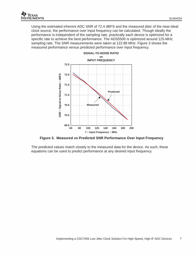
In the case of the ADS5500, the baseline performance measured with a low jitter HP8644Bsignal generator and narrow band-pass filter yields an SNR value around 71.5 dBFS at 100 MHzwith the input signal at −1 dBFS. The clock source was measured independently and shown tohave approximately 0.25-ps RMS jitter over 1 kHz to 40 MHz. Using the full-scale value of theADS5500 which is 2.3 Vpp at 100-MHz input frequency and driving the ADC to −1 dBFS, theSNR contribution from the near-ideal clock source is 78.9 dBFS. Given this information and themeasured total SNR measurements, the inherent SNR of the ADC is estimated using theequation above to be 72.4 dBFS.
SLWA034
7 Implementing a CDC7005 Low Jitter Clock Solution For High-Speed, High-IF ADC Devices
Using the estimated inherent ADC SNR of 72.4 dBFS and the measured jitter of the near-idealclock source, the performance over input frequency can be calculated. Though ideally theperformance is independent of the sampling rate, practically each device is optimized for aspecific rate to achieve the best performance. The ADS5500 is optimized around 125-MHzsampling rate. The SNR measurements were taken at 122.88 MHz. Figure 3 shows themeasured performance versus predicted performance over input frequency.
f − Input Frequency − MHz
69.5
70.0
70.5
71.0
71.5
72.0
72.5
60 80 100 120 140 160 180 200
SN
R −
Sig
nal-t
o-N
oise
Rat
io −
dB
FS
SIGNAL-TO-NOISE RATIOvs
INPUT FREQUENCY
Measured
Predicted
Figure 3. Measured vs Predicted SNR Performance Over Input Frequency
The predicted values match closely to the measured data for the device. As such, theseequations can be used to predict performance at any desired input frequency.
SLWA034
8 Implementing a CDC7005 Low Jitter Clock Solution For High-Speed, High-IF ADC Devices
3 Effect of Clock Amplitude
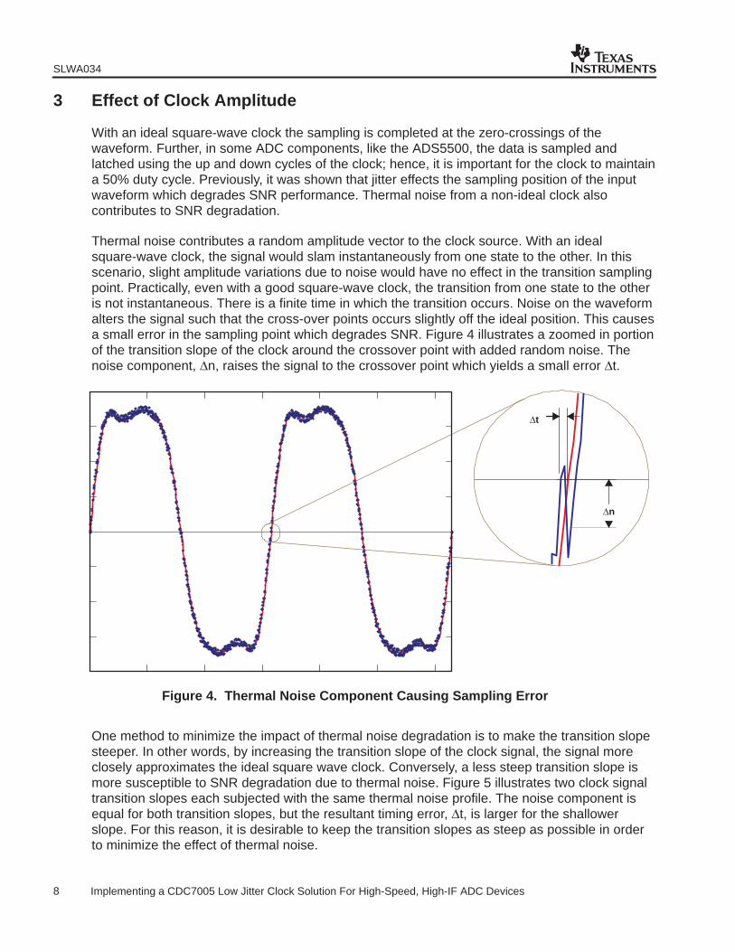
With an ideal square-wave clock the sampling is completed at the zero-crossings of thewaveform. Further, in some ADC components, like the ADS5500, the data is sampled andlatched using the up and down cycles of the clock; hence, it is important for the clock to maintaina 50% duty cycle. Previously, it was shown that jitter effects the sampling position of the inputwaveform which degrades SNR performance. Thermal noise from a non-ideal clock alsocontributes to SNR degradation.
Thermal noise contributes a random amplitude vector to the clock source. With an idealsquare-wave clock, the signal would slam instantaneously from one state to the other. In thisscenario, slight amplitude variations due to noise would have no effect in the transition samplingpoint. Practically, even with a good square-wave clock, the transition from one state to the otheris not instantaneous. There is a finite time in which the transition occurs. Noise on the waveformalters the signal such that the cross-over points occurs slightly off the ideal position. This causesa small error in the sampling point which degrades SNR. Figure 4 illustrates a zoomed in portionof the transition slope of the clock around the crossover point with added random noise. Thenoise component, ∆n, raises the signal to the crossover point which yields a small error ∆t.
∆n
∆t
Figure 4. Thermal Noise Component Causing Sampling Error
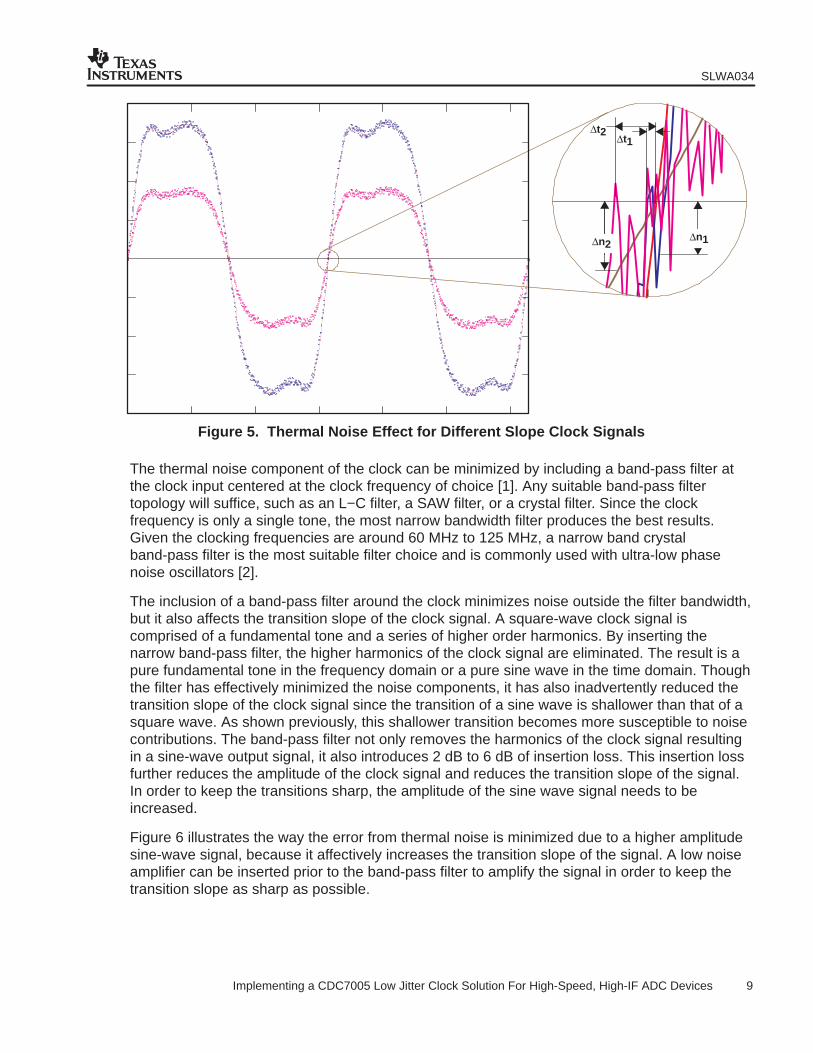
One method to minimize the impact of thermal noise degradation is to make the transition slopesteeper. In other words, by increasing the transition slope of the clock signal, the signal moreclosely approximates the ideal square wave clock. Conversely, a less steep transition slope ismore susceptible to SNR degradation due to thermal noise. Figure 5 illustrates two clock signaltransition slopes each subjected with the same thermal noise profile. The noise component isequal for both transition slopes, but the resultant timing error, ∆t, is larger for the shallowerslope. For this reason, it is desirable to keep the transition slopes as steep as possible in orderto minimize the effect of thermal noise.
SLWA034
9 Implementing a CDC7005 Low Jitter Clock Solution For High-Speed, High-IF ADC Devices
∆t2∆t1
∆n2∆n1
Figure 5. Thermal Noise Effect for Different Slope Clock Signals
The thermal noise component of the clock can be minimized by including a band-pass filter atthe clock input centered at the clock frequency of choice [1]. Any suitable band-pass filtertopology will suffice, such as an L−C filter, a SAW filter, or a crystal filter. Since the clockfrequency is only a single tone, the most narrow bandwidth filter produces the best results.Given the clocking frequencies are around 60 MHz to 125 MHz, a narrow band crystalband-pass filter is the most suitable filter choice and is commonly used with ultra-low phasenoise oscillators [2].
The inclusion of a band-pass filter around the clock minimizes noise outside the filter bandwidth,but it also affects the transition slope of the clock signal. A square-wave clock signal iscomprised of a fundamental tone and a series of higher order harmonics. By inserting thenarrow band-pass filter, the higher harmonics of the clock signal are eliminated. The result is apure fundamental tone in the frequency domain or a pure sine wave in the time domain. Thoughthe filter has effectively minimized the noise components, it has also inadvertently reduced thetransition slope of the clock signal since the transition of a sine wave is shallower than that of asquare wave. As shown previously, this shallower transition becomes more susceptible to noisecontributions. The band-pass filter not only removes the harmonics of the clock signal resultingin a sine-wave output signal, it also introduces 2 dB to 6 dB of insertion loss. This insertion lossfurther reduces the amplitude of the clock signal and reduces the transition slope of the signal.In order to keep the transitions sharp, the amplitude of the sine wave signal needs to beincreased.
Figure 6 illustrates the way the error from thermal noise is minimized due to a higher amplitudesine-wave signal, because it affectively increases the transition slope of the signal. A low noiseamplifier can be inserted prior to the band-pass filter to amplify the signal in order to keep thetransition slope as sharp as possible.

SLWA034
10 Implementing a CDC7005 Low Jitter Clock Solution For High-Speed, High-IF ADC Devices
∆t2∆t1
∆n
Figure 6. Thermal Noise Effect for Different Amplitude Sinusoids
4 CDC7005 Clocking Solution
The CDC7005 is a high performance, low jitter differential clock driver and clock distributionchip. It has five independently controlled outputs, which can be suitably used to clock highperformance ADCs like the ADS5500, as well as satisfy other clocking requirements on theboard. The CDC7005 offers a real-world clocking solution for these applications, which cansynchronize the clock output to a supplied board reference frequency.
The CDC7005 device’s key features are:
1. The reference clock can be synchronized to virtually any VCXO frequency.
2. Reference clock jitter is cleaned
3. Low jitter output
4. Five independent frequency outputs selectable by /2n
5. Differential LVPECL interface
SLWA034
11 Implementing a CDC7005 Low Jitter Clock Solution For High-Speed, High-IF ADC Devices
5 CDC7005 Design Considerations
5.1 VCXO Requirement
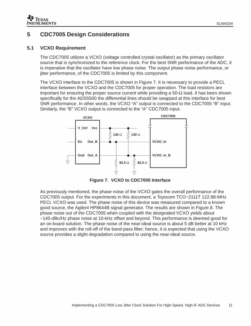
The CDC7005 utilizes a VCXO (voltage controlled crystal oscillator) as the primary oscillatorsource that is synchronized to the reference clock. For the best SNR performance of the ADC, itis imperative that the oscillator have low phase noise. The output phase noise performance, orjitter performance, of the CDC7005 is limited by this component.
The VCXO interface to the CDC7005 is shown in Figure 7. It is necessary to provide a PECLinterface between the VCXO and the CDC7005 for proper operation. The load resistors areimportant for ensuring the proper source current while providing a 50-Ω load. It has been shownspecifically for the ADS5500 the differential lines should be swapped at this interface for bestSNR performance. In other words, the VCXO “A” output is connected to the CDC7005 “B” input.Similarly, the “B” VCXO output is connected to the “A” CDC7005 input.
VccV_Ctrl
VCXO
Out_BEn
130 Ω
82.5 Ω
Out_AGnd
130 Ω
82.5 Ω
CDC7005
VCXO_In
VCXO_In_B
Figure 7. VCXO to CDC7005 Interface
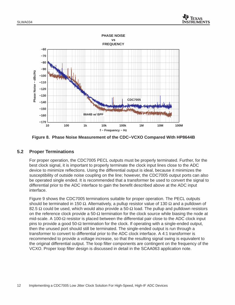
As previously mentioned, the phase noise of the VCXO gates the overall performance of theCDC7005 output. For the experiments in this document, a Toyocom TCO−2111T 122.88-MHzPECL VCXO was used. The phase noise of this device was measured compared to a knowngood source, the Agilent HP8644B signal generator. The results are shown in Figure 8. Thephase noise out of the CDC7005 when coupled with the designated VCXO yields about −145-dBc/Hz phase noise at 10-kHz offset and beyond. This performance is deemed good foran on-board solution. The phase noise of the near-ideal source is about 5 dB better at 10 kHzand improves with the roll-off of the band-pass filter; hence, it is expected that using the VCXOsource provides a slight degradation compared to using the near-ideal source.
SLWA034
12 Implementing a CDC7005 Low Jitter Clock Solution For High-Speed, High-IF ADC Devices
f − Frequency − Hz
−170
−160
−150
−140
−130
−120
−110
−100
−90
−80
−70
−60
Pha
se N
oise
− d
Bc/
Hz
PHASE NOISEvs
FREQUENCY
CDC7005
8644B w/ BPF
10 100 1k 100M10k 100k 1M 10M
Figure 8. Phase Noise Measurement of the CDC−VCXO Compared With HP8644B
5.2 Proper Terminations
For proper operation, the CDC7005 PECL outputs must be properly terminated. Further, for thebest clock signal, it is important to properly terminate the clock input lines close to the ADCdevice to minimize reflections. Using the differential output is ideal, because it minimizes thesusceptibility of outside noise coupling on the line; however, the CDC7005 output ports can alsobe operated single ended. It is recommended that a transformer be used to convert the signal todifferential prior to the ADC interface to gain the benefit described above at the ADC inputinterface.
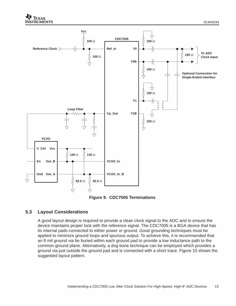
Figure 9 shows the CDC7005 terminations suitable for proper operation. The PECL outputsshould be terminated in 150 Ω. Alternatively, a pullup resistor value of 130 Ω and a pulldown of82.5 Ω could be used, which would also provide a 50-Ω load. The pullup and pulldown resistorson the reference clock provide a 50-Ω termination for the clock source while biasing the node atmid-scale. A 100-Ω resistor is placed between the differential pair close to the ADC clock inputpins to provide a good 50-Ω termination for the clock. If operating with a single-ended output,then the unused port should still be terminated. The single-ended output is run through atransformer to convert to differential prior to the ADC clock interface. A 4:1 transformer isrecommended to provide a voltage increase, so that the resulting signal swing is equivalent tothe original differential output. The loop filter components are contingent on the frequency of theVCXO. Proper loop filter design is discussed in detail in the SCAA063 application note.
SLWA034
13 Implementing a CDC7005 Low Jitter Clock Solution For High-Speed, High-IF ADC Devices
VccV_Ctrl
VCXO
Out_BEn
130 Ω
82.5 Ω
Out_AGnd
130 Ω
82.5 Ω
Loop Filter
Ref_in
CDC7005
Y0
Cp_Out
150 Ω
100 Ω
Y0B
To ADCClock Inpu t
150 Ω
Y1
150 Ω
Y1B
150 Ω
100 Ω
100 Ω
Vcc
Reference Clock
VCXO_In
VCXO_In_B
Optional Connection forSingle-Ended Interface
Figure 9. CDC7005 Terminations
5.3 Layout Considerations
A good layout design is required to provide a clean clock signal to the ADC and to ensure thedevice maintains proper lock with the reference signal. The CDC7005 is a BGA device that hasits internal pads connected to either power or ground. Good grounding techniques must beapplied to minimize ground loops and spurious output. To achieve this, it is recommended thatan 8 mil ground via be buried within each ground pad to provide a low inductance path to thecommon ground plane. Alternatively, a dog bone technique can be employed which provides aground via just outside the ground pad and is connected with a short trace. Figure 10 shows thesuggested layout pattern.

SLWA034
14 Implementing a CDC7005 Low Jitter Clock Solution For High-Speed, High-IF ADC Devices
SupplyPads
0.80 mm 0.50 mm
0.008 in
Grid Pattern Dog-Bone Pattern
Ground Pads
0.80 mm
5.60 mm
Figure 10. Grounding and Supply Connection Schemes for the CDC7005
It is also important to provide good bypassing of the supplies close to the supply pins of theCDC7005 device. This ensures a good low impedance path to the ground plane for any noise orspurious signals on the supply, which helps provide a cleaner clock for the ADC. Small vias areplaced in or close to the supply pads, similar to the ground vias, to provide a direct path to aninternal power plane layer. Small 0402 size 0.1-µF capacitors are placed on the opposite side ofthe board from the device and connect to the existing supply and ground vias to provide supplybypassing.
Figure 11 shows the bypassing pattern that is recommended for the components placed insidethe grid pattern. Additional supply bypassing, including larger value capacitors for lowerfrequency bypassing, is recommended and should be placed close to the device but outside thegrid pattern as is conducive for the layout; these bypassing components are not shown in thefigures.

SLWA034
15 Implementing a CDC7005 Low Jitter Clock Solution For High-Speed, High-IF ADC Devices
0.008 in0402
BypassCapacitor
Ground Plane
Figure 11. Supply Bypassing for the CDC7005
6 CDC7005 Clock Source for the ADS5500
To illustrate the performance of the CDC7005 clocking solution, the device is coupled with theToyocom 122.88-MHz VCXO and used to supply the clock signal to the ADS5500. The data iscompared to the baseline performance using an extremely good phase-noise generator with acrystal band-pass filter. The test setup is shown in Figure 12.
ADS5500
IF inClk
14
LogicAnalyzer
HP8644Bor Equivalent
RefClk
HP8644Bor Equivalent
Ref
Figure 12. ADC Evaluation Test Set Up (Baseline)
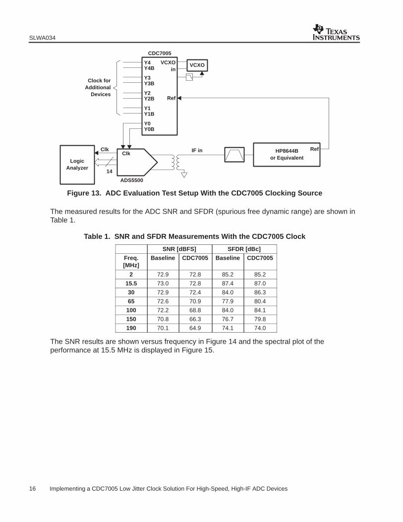
The measured performance of the device over frequency with near-ideal clock source iscompared to the performance utilizing the CDC7005 as a clock source. The block diagram of theADC test set up incorporating the CDC7005 is shown in Figure 13.
SLWA034
16 Implementing a CDC7005 Low Jitter Clock Solution For High-Speed, High-IF ADC Devices
Clock forAdditional
Devices
ADS5500
IF inClk
14
VCXO
Y0Y0B
Y1Y1B
Y2Y2B
Y3Y3B
Y4Y4B
Ref
VCXOin
CDC7005
LogicAnalyzer
HP8644Bor Equivalent
RefClk
Figure 13. ADC Evaluation Test Setup With the CDC7005 Clocking Source
The measured results for the ADC SNR and SFDR (spurious free dynamic range) are shown inTable 1.
Table 1. SNR and SFDR Measurements With the CDC7005 Clock
SNR [dBFS] SFDR [dBc]
Freq.[MHz]
Baseline CDC7005 Baseline CDC7005
2 72.9 72.8 85.2 85.2
15.5 73.0 72.8 87.4 87.0
30 72.9 72.4 84.0 86.3
65 72.6 70.9 77.9 80.4
100 72.2 68.8 84.0 84.1
150 70.8 66.3 76.7 79.8
190 70.1 64.9 74.1 74.0
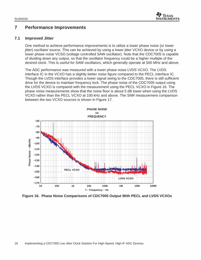
The SNR results are shown versus frequency in Figure 14 and the spectral plot of theperformance at 15.5 MHz is displayed in Figure 15.
SLWA034
17 Implementing a CDC7005 Low Jitter Clock Solution For High-Speed, High-IF ADC Devices
f − Input Frequency − MHz
64
65
66
67
68
69
70
71
72
73
74
0 20 40 60 80 100 120 140 160 180 200
SN
R −
Sig
nal-t
o-N
oise
Rat
io −
dB
FS
SIGNAL-TO-NOISE RATIOvs
INPUT FREQUENCY
CDC7005
Baseline
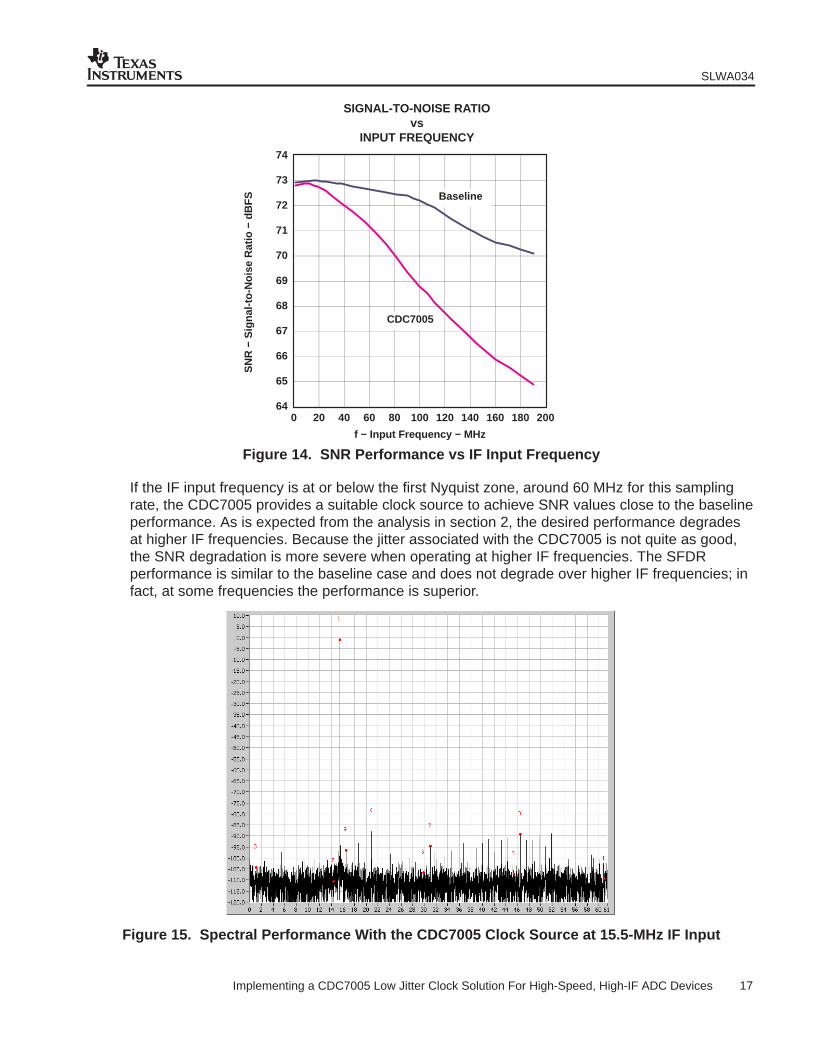
Figure 14. SNR Performance vs IF Input Frequency
If the IF input frequency is at or below the first Nyquist zone, around 60 MHz for this samplingrate, the CDC7005 provides a suitable clock source to achieve SNR values close to the baselineperformance. As is expected from the analysis in section 2, the desired performance degradesat higher IF frequencies. Because the jitter associated with the CDC7005 is not quite as good,the SNR degradation is more severe when operating at higher IF frequencies. The SFDRperformance is similar to the baseline case and does not degrade over higher IF frequencies; infact, at some frequencies the performance is superior.
Figure 15. Spectral Performance With the CDC7005 Clock Source at 15.5-MHz IF Input
SLWA034
18 Implementing a CDC7005 Low Jitter Clock Solution For High-Speed, High-IF ADC Devices
7 Performance Improvements
7.1 Improved Jitter
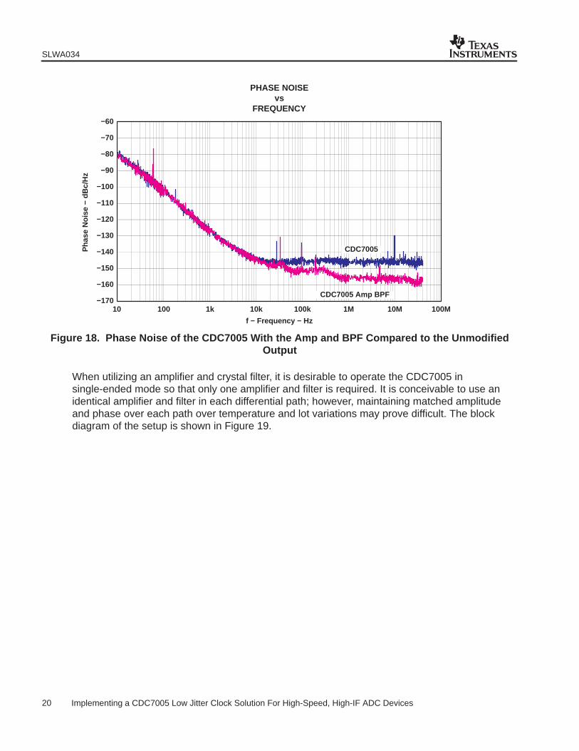
One method to achieve performance improvements is to utilize a lower phase noise (or lowerjitter) oscillator source. This can be achieved by using a lower jitter VCXO device or by using alower phase noise VCSO (voltage controlled SAW oscillator). Note that the CDC7005 is capableof dividing down any output, so that the oscillator frequency could be a higher multiple of thedesired clock. This is useful for SAW oscillators, which generally operate at 500 MHz and above.
The ADC performance was measured with a lower phase noise LVDS VCXO. The LVDSinterface IC in the VCXO has a slightly better noise figure compared to the PECL interface IC.Though the LVDS interface provides a lower signal swing to the CDC7005, there is still sufficientdrive for the device to maintain frequency lock. The phase noise of the CDC7005 output usingthe LVDS VCXO is compared with the measurement using the PECL VCXO in Figure 16. Thephase noise measurements show that the noise floor is about 5 dB lower when using the LVDSVCXO rather than the PECL VCXO at 100 kHz and above. The SNR measurement comparisonbetween the two VCXO sources is shown in Figure 17.
f − Frequency − Hz
−170
−160
−150
−140
−130
−120
−110
−100
−90
−80
−70
−60
Pha
se N
oise
− d
Bc/
Hz
PHASE NOISEvs
FREQUENCY
10 100 1k 100M10k 100k 1M 10M
PECL VCXO
LVDS VCXO
Figure 16. Phase Noise Comparisons of CDC7005 Output With PECL and LVDS VCXOs

SLWA034
19 Implementing a CDC7005 Low Jitter Clock Solution For High-Speed, High-IF ADC Devices
f − Input Frequency − MHz
63
64
65
66
67
68
69
70
71
72
60 80 100 120 140 160 180 200
SN
R −
Sig
nal-t
o-N
oise
Rat
io −
dB
FS
SIGNAL-TO-NOISE RATIOvs
INPUT FREQUENCY
PECL VCXO
LVDS VCXO
Figure 17. SNR Improvement With Lower Phase Noise VCXO Source
The improved phase noise oscillator yielded as much as 1.5-dB SNR improvement at the high IFinput signals. The results show that any phase noise improvement from the oscillator sourcegenerally transfers to better SNR performance from the ADC. Though the SNR performance hasimproved at the high IF inputs, it is still not on par with the baseline measurements; furtherimprovements are required.
7.2 Lower Thermal Noise
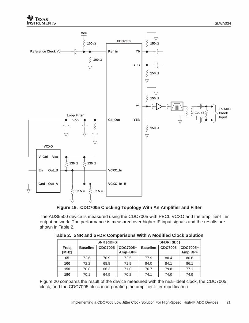
As seen in section 3, minimizing thermal noise on the clock improves the phase noise andimproves the SNR performance. This is achieved by placing a narrow band crystal filter after theCDC7005 output. The filter used is a Toyocom TF2−C2EC1 122.88-MHz crystal filter withapproximately 20 kHz of total bandwidth. The crystal filter is matched to 50 Ω to provide asuitable interface to the other circuitry. The crystal filter introduces about 3 dB of insertion loss.As previously discussed, the combination of the filter’s insertion loss and conversion from asquare wave output to a sine wave output reduces the transition slope of the clock waveform.The benefit of the added filter is negated by the insertion loss and the loss of square wave.Adding a small broadband amplifier stage just prior to the filter compensates for the loss of thefilter and provides steep clock transitions. Though the filter attenuates much of the broadbandnoise from the amplifier, noise within the filter’s pass band still gets through. It is a good designpractice to keep the noise figure of the booster amplifier to less than 3 dB.
The phase noise of the CDC7005 (with PECL VCXO) coupled with the amplifier and filter isshown in Figure 18. Below the corner frequency of the band-pass filter, the performancebetween the two cases is nearly identical. Once the corner frequency is reached, the phasenoise improves. After 100-kHz offset, the phase noise performance of the CDC7005−Amp−BPFcombination rivals that of the near-ideal source.
SLWA034
20 Implementing a CDC7005 Low Jitter Clock Solution For High-Speed, High-IF ADC Devices
f − Frequency − Hz
−170
−160
−150
−140
−130
−120
−110
−100
−90
−80
−70
−60
Pha
se N
oise
− d
Bc/
Hz
PHASE NOISEvs
FREQUENCY
10 100 1k 100M10k 100k 1M 10M
CDC7005
CDC7005 Amp BPF
Figure 18. Phase Noise of the CDC7005 With the Amp and BPF Compared to the UnmodifiedOutput
When utilizing an amplifier and crystal filter, it is desirable to operate the CDC7005 insingle-ended mode so that only one amplifier and filter is required. It is conceivable to use anidentical amplifier and filter in each differential path; however, maintaining matched amplitudeand phase over each path over temperature and lot variations may prove difficult. The blockdiagram of the setup is shown in Figure 19.
SLWA034
21 Implementing a CDC7005 Low Jitter Clock Solution For High-Speed, High-IF ADC Devices
VccV_Ctrl
VCXO
Out_BEn
130 Ω
82.5 Ω
Out_AGnd
130 Ω
82.5 Ω
Loop Filter
Ref_in
CDC7005
Y0
Cp_Out
150 Ω
100 Ω
Y0B
To ADCClockInput
150 Ω
Y1
150 Ω
Y1B
150 Ω
100 Ω
100 Ω
Vcc
Reference Clock
VCXO_In
VCXO_In_B
Figure 19. CDC7005 Clocking Topology With An Amplifier and Filter
The ADS5500 device is measured using the CDC7005 with PECL VCXO and the amplifier-filteroutput network. The performance is measured over higher IF input signals and the results areshown in Table 2.
Table 2. SNR and SFDR Comparisons With A Modified Clock Solution SNR [dBFS] SFDR [dBc]
Freq.[MHz]
Baseline CDC7005 CDC7005−Amp−BPF
Baseline CDC7005 CDC7005−Amp BPF
65 72.6 70.9 72.5 77.9 80.4 80.6
100 72.2 68.8 71.9 84.0 84.1 86.1
150 70.8 66.3 71.0 76.7 79.8 77.1
190 70.1 64.9 70.2 74.1 74.0 74.9
Figure 20 compares the result of the device measured with the near-ideal clock, the CDC7005clock, and the CDC7005 clock incorporating the amplifier-filter modification.
SLWA034
22 Implementing a CDC7005 Low Jitter Clock Solution For High-Speed, High-IF ADC Devices
f − Input Frequency − MHz
64
65
66
67
68
69
70
71
72
73
60 80 100 120 140 160 180 200
SN
R −
Sig
nal-t
o-N
oise
Rat
io −
dB
FS
SIGNAL-TO-NOISE RATIOvs
INPUT FREQUENCY
CDC7005
CDC7005 Amp BPF
Baseline
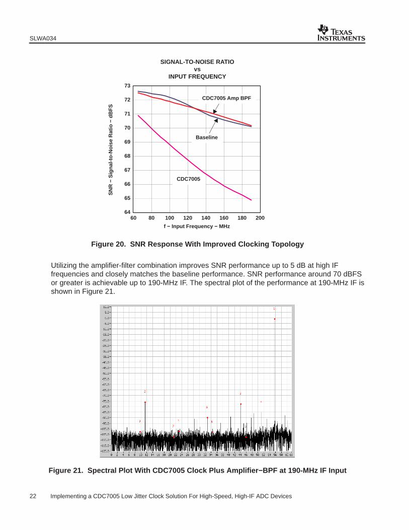
Figure 20. SNR Response With Improved Clocking Topology
Utilizing the amplifier-filter combination improves SNR performance up to 5 dB at high IFfrequencies and closely matches the baseline performance. SNR performance around 70 dBFSor greater is achievable up to 190-MHz IF. The spectral plot of the performance at 190-MHz IF isshown in Figure 21.
Figure 21. Spectral Plot With CDC7005 Clock Plus Amplifier−BPF at 190-MHz IF Input
SLWA034
23 Implementing a CDC7005 Low Jitter Clock Solution For High-Speed, High-IF ADC Devices
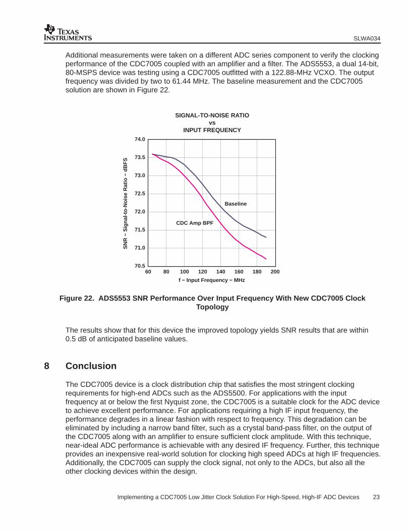
Additional measurements were taken on a different ADC series component to verify the clockingperformance of the CDC7005 coupled with an amplifier and a filter. The ADS5553, a dual 14-bit,80-MSPS device was testing using a CDC7005 outfitted with a 122.88-MHz VCXO. The outputfrequency was divided by two to 61.44 MHz. The baseline measurement and the CDC7005solution are shown in Figure 22.
f − Input Frequency − MHz
70.5
71.0
71.5
72.0
72.5
73.0
73.5
74.0
60 80 100 120 140 160 180 200
SN
R −
Sig
nal-t
o-N
oise
Rat
io −
dB
FS
SIGNAL-TO-NOISE RATIOvs
INPUT FREQUENCY
CDC Amp BPF
Baseline
Figure 22. ADS5553 SNR Performance Over Input Frequency With New CDC7005 ClockTopology
The results show that for this device the improved topology yields SNR results that are within0.5 dB of anticipated baseline values.
8 Conclusion
The CDC7005 device is a clock distribution chip that satisfies the most stringent clockingrequirements for high-end ADCs such as the ADS5500. For applications with the inputfrequency at or below the first Nyquist zone, the CDC7005 is a suitable clock for the ADC deviceto achieve excellent performance. For applications requiring a high IF input frequency, theperformance degrades in a linear fashion with respect to frequency. This degradation can beeliminated by including a narrow band filter, such as a crystal band-pass filter, on the output ofthe CDC7005 along with an amplifier to ensure sufficient clock amplitude. With this technique,near-ideal ADC performance is achievable with any desired IF frequency. Further, this techniqueprovides an inexpensive real-world solution for clocking high speed ADCs at high IF frequencies.Additionally, the CDC7005 can supply the clock signal, not only to the ADCs, but also all theother clocking devices within the design.

SLWA034
24 Implementing a CDC7005 Low Jitter Clock Solution For High-Speed, High-IF ADC Devices
9 References1. Zanchi, A., Papantonopoulos, I., Tsay, F., Measurement and Spice Prediction of
Sub-PicoSecond Clock Jitter in A/D Converters, Proceedings of ISCAS 2003, May 2003
2. http://www.sigtech.com/olektron/pdf_newproducts/TK951TechnicalFeature.pdf
3. Electronic Design, Pay Attention to the Clock and Output Bus to Improve High Speed ADCDesigns, June 26, 2000
4. General Guideline: CDC7005 as a Clock Synthesizer and Jitter Cleaner, Texas Instrumentsapplication note (SCA063)
5. Lee, Steve & Yang, Ken, Design a Low−Jitter Clock for High Speed A/D Converters, SensorTechnology and Design, Vol. 18, No. 10, October 2001
6. Beckemeyer, Heinz-Peter, Analog-to-Digital Converters Support Multicarrier Systems, WirelessEurope, February 2004

IMPORTANT NOTICE
Texas Instruments Incorporated and its subsidiaries (TI) reserve the right to make corrections, modifications,enhancements, improvements, and other changes to its products and services at any time and to discontinueany product or service without notice. Customers should obtain the latest relevant information before placingorders and should verify that such information is current and complete. All products are sold subject to TI’s termsand conditions of sale supplied at the time of order acknowledgment.
TI warrants performance of its hardware products to the specifications applicable at the time of sale inaccordance with TI’s standard warranty. Testing and other quality control techniques are used to the extent TIdeems necessary to support this warranty. Except where mandated by government requirements, testing of allparameters of each product is not necessarily performed.
TI assumes no liability for applications assistance or customer product design. Customers are responsible fortheir products and applications using TI components. To minimize the risks associated with customer productsand applications, customers should provide adequate design and operating safeguards.
TI does not warrant or represent that any license, either express or implied, is granted under any TI patent right,copyright, mask work right, or other TI intellectual property right relating to any combination, machine, or processin which TI products or services are used. Information published by TI regarding third-party products or servicesdoes not constitute a license from TI to use such products or services or a warranty or endorsement thereof.Use of such information may require a license from a third party under the patents or other intellectual propertyof the third party, or a license from TI under the patents or other intellectual property of TI.
Reproduction of information in TI data books or data sheets is permissible only if reproduction is withoutalteration and is accompanied by all associated warranties, conditions, limitations, and notices. Reproductionof this information with alteration is an unfair and deceptive business practice. TI is not responsible or liable forsuch altered documentation.
Resale of TI products or services with statements different from or beyond the parameters stated by TI for thatproduct or service voids all express and any implied warranties for the associated TI product or service andis an unfair and deceptive business practice. TI is not responsible or liable for any such statements.
Following are URLs where you can obtain information on other Texas Instruments products and applicationsolutions:
Products Applications
Amplifiers amplifier.ti.com Audio www.ti.com/audio
Data Converters dataconverter.ti.com Automotive www.ti.com/automotive
DSP dsp.ti.com Broadband www.ti.com/broadband
Interface interface.ti.com Digital Control www.ti.com/digitalcontrol
Logic logic.ti.com Military www.ti.com/military
Power Mgmt power.ti.com Optical Networking www.ti.com/opticalnetwork
Microcontrollers microcontroller.ti.com Security www.ti.com/security
Telephony www.ti.com/telephony
Video & Imaging www.ti.com/video
Wireless www.ti.com/wireless
Mailing Address: Texas Instruments
Post Office Box 655303 Dallas, Texas 75265
Copyright 2004, Texas Instruments Incorporated