design methodology for low-jitter differential clock...
TRANSCRIPT
Design methodology for low-jitter differential clock recovery circuits in high performance ADCs
Juan Núñez, Antonio J. Ginés, Eduardo J. Peralías, Adoración Rueda Instituto de Microelectrónica de Sevilla, IMSE-CNM (CSIC/Universidad de Sevilla)
Av. Américo Vespucio s/n 41092, Seville (Spain) Emails: {jnunez,gines,peralias,rueda}@imse-cnm.csic.es
Abstract— This paper presents a design methodology for the simultaneous optimization of jitter and power consumption in ultra-low jitter clock recovery circuits (<100fsrms) for high-performance ADCs. The key ideas of the design methodology are: a) a smart parameterization of transistor sizes to have smooth dependence of specifications on the design variables, b) based on this parameterization, carrying out a design space sub-sampling which allows capturing the whole circuit performance for reducing computation resources and time during optimization. The proposed methodology, which can easily incorporate process voltage and temperature (PVT) variations, has been used to perform a systematic design space exploration that provides sub-100fs jitter clock recovery circuits in two CMOS commercial processes at different technological nodes (1.8V 0.18µm and 1.2V 90nm). Post-layout simulation results for a case of study with typical jitter of 68fs for a 1.8V 80dB-SNDR 100Msps Pipeline ADC application are also shown as demonstrator.
Keywords — Clock recovery, ultra-low jitter, design methodology, high-speed high-resolution ADCs, Pipeline ADCs.
I. INTRODUCTION
In many recent electronics systems there is a continuous trend to replace analog circuitry by their digital counterparts, which involves increasing the process and storage of data in the digital domain. One of the keys to success of these systems is the rapid evolution of analog to digital converters (ADC) for translating continuous-time signal information to discrete-data with great performance [1]. Such cutting-edge applications will require high resolution ADCs (12 bits or more) at high sampling rates from several tens of MHz up to GHz. Unluckily, effective resolution of the ADC decreases with the sampling rate and input frequency, and thus, a trade-off between accuracy and speed exists. Among the different error sources which contribute to this degradation, clock jitter is a fundamental limiting factor at high-frequencies inputs. The sensitivity to the jitter effect is especially critical for software radio applications in which the upper order n-th Nyquist Bands are directly down converted by the sampling stage at the front-end of the ADC, acting as a discrete time mixer (IF-sampling).
A clock signal that has variations in the duration of its period or duty cycle is said to exhibit jitter. Clock jitter causes an uncertainty in the precise sampling time, resulting in a reduction of the ADC resolution [2]. Thus, the digitization of high speed signals requires an appropriate low-jitter reconstruction of the clock in order to fulfill the sampling performance, typically above 2 effective bits over the target specification, to provide safety margin for other errors in the system (thermal noise, incomplete settling, static non-linerities, etc.). As an example, assuming that the jitter is the unique source of error, values under 80fs are necessary to obtain a specific effective number of bits due to jitter (ENOBjitter) of 14.0 bits at input frequencies above 100MHz. The same jitter level is required to have an ENOBjitter of 15.0 bits at 50MHz.
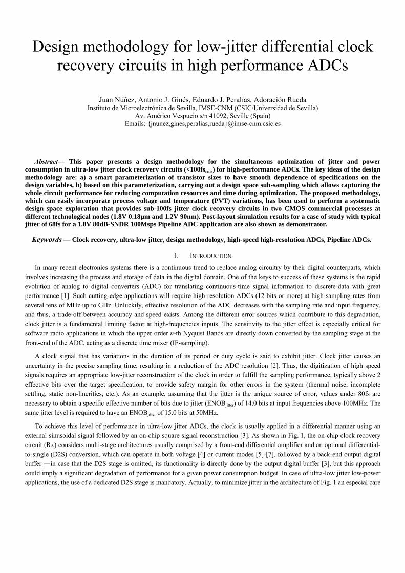
To achieve this level of performance in ultra-low jitter ADCs, the clock is usually applied in a differential manner using an external sinusoidal signal followed by an on-chip square signal reconstruction [3]. As shown in Fig. 1, the on-chip clock recovery circuit (Rx) considers multi-stage architectures usually comprised by a front-end differential amplifier and an optional differential-to-single (D2S) conversion, which can operate in both voltage [4] or current modes [5]-[7], followed by a back-end output digital buffer ―in case that the D2S stage is omitted, its functionality is directly done by the output digital buffer [3], but this approach could imply a significant degradation of performance for a given power consumption budget. In case of ultra-low jitter low-power applications, the use of a dedicated D2S stage is mandatory. Actually, to minimize jitter in the architecture of Fig. 1 an especial care

should be paid to D2S stage performing the fundamental task of clock signal reconstruction, since its operation has a great impact on the clock edge slopes, as well as on the specific gain distributions among stages. In [4], a theoretical analysis of the optimum gain distributions for a target jitter is presented, but trade-offs with power consumption are not explicitly considered and, therefore, it relies on the expertise of the designer. This approach could lead to non-optimum designs in terms of power, even eventually leading to no solutions when strong constrains between specifications are present.
The situation could be even more difficult when dealing with process voltage and temperature (PVT) variations in presence of post-layout parasitics, making the design of ultra-low-jitter recovery circuit quite challenging. In the last decade, a huge improvement in automatic design methodologies for basic analog building blocks (op-amps, low-noise amplifiers or regulators) has been carried out [9]. These methods rely on optimization routines (acting as search engine), such as evolutionary [10] or simulated annealing [11] algorithms, to perform automatic sizing of building blocks based on transistor-level simulations. The target specifications are often derived from the operating point (OP) and small signal AC analysis, typically including finite DC-gain, bandwidth or slew-rate at low hierarchical level. For circuit systems, comprised by multiple building blocks, sizing at transistor-level from raw could not result efficient in terms of computation time, since long transient simulations which incorporate great signal effects could be necessary to evaluate target metrics (power, total harmonic distortion, accuracy, effective number of bits, noise, etc.), making necessary the inclusion of intelligence in the automatic design process even for relative simple cases of study [12]. The extension to more complex systems in terms of number of components and/or specification set implies a change in the methodology paradigm from a force-brute simulation-based strategy in which the transistor sizes are randomly selected at the initial phases (later optimized by the search engine) to methodologies in which the design expertise is incorporated in the process from the very beginning [13]. The idea of these techniques is to minimize the computation time reducing the number of initial design candidates to be explored to only those that have a minimum chance of success from the point of view of an efficient analog design ―that is, enough voltage overdrive in specific transistors, right operating point in nominal biasing conditions, matching requirements between circuit branches, etc.
Taking into account this second approach, in this work a design methodology for the simultaneous optimization of jitter and power consumption in ultra-low jitter clock recovery circuits for high-performance applications is proposed [14]. The design methodology allows a systematic exploration of the design space through a strategy to find competitive trade-offs between jitter and power consumption. Following this strategy, process voltage and temperature (PVT) variations can be incorporated to guarantee that target requirements are satisfied in all technological corners. The method is fully general and can be applied to typical clock recovery circuits, such as those found in [3]-[7], and different process technologies. Transistor-level results in two CMOS commercial processes at different technological nodes (1.8V 0.18µm, and 1.2V 90nm) are presented as validation. Post-layout simulations results for a practical case with 68fs for a 1.8V 2Vpp 80dB-SNDR 100Msps Pipeline ADC application are also shown as demonstrator.
Contents in this paper are distributed as follows. In Section II a brief review about the jitter effects and the clock regeneration in ultra-low jitter applications is carried out with emphasis on practical implementations at both system and circuit levels. Several
Fig. 1 Simplified block diagram of a possible scheme for ultra-low-jitter clock recovery with details on the on-chip multistage clock recovery circuit.

transistor topologies for the clock receiver front-end (Rx) are analyzed. In Section III the proposed methodology for the design of low-jitter differential clock recovery circuits is presented. For sake of clarification, without lack of generality, the main concepts in this methodology will be illustrated using the clock recovery circuit with embedded current-mode D2S stage proposed in [7]. In Section IV, the methodology is applied to the transistor-level implementations introduced in Section II, making a comparison between them in two CMOS commercial processes at different technological nodes (1.8V 0.18µm and 1.2V 90nm). Simulation results for post-layout simulations using this case of study are provided in Section V. Finally, conclusions are given in Section VI.
II. ULTRA-LOW JITTER CLOCK RECOVERY CIRCUITS
A. Jitter Effects and Modelling
High-speed high-resolution ADCs require as mentioned before a low-phase noise (low jitter) clock in order to limit the dynamic performance degradation. The clock jitter is defined as the sample to sample variation in aperture delay of the clock, that is, when the input signal is actually sampled with respect to the sampling clock edge. The sampling instants are determined by the edges of the clock signal. However these clock edges can vary from cycle to cycle due to imperfections of the circuit and time-variant random noise sources and, therefore, cause voltage errors at the sampling points. As illustrated in Fig. 2a, the desired sampling instant, tS, turns into tS+ΔtJ. The error can be approximated at first order as follows:
( ) ( ( )) ( ) ( )S
J S S J S S J St t
dxx t x t t t x t t t
dt
(1)
where { ( )}J kt t is the sequence of clock jitter of sampling edges associated to the sampling process.
Assuming a sinusoidal wave input, x(t), with amplitude Ain and a frequency fin, the error is maximum at the zero crossing points
( ) 2 max{ }J in in JMAX tx t A f t . If the clock jitter is assumed a zero mean random noise with standard deviation 2( )JJ t ,
then the sampling error power due to jitter can be approximated by:
2
2 2 2 2 2 2 2 2 2_ ,
1( ) (2 ) cos (2 ) (2 )
2k
samp error J J in in in k in int
dxP x J J A f f t f A J
dt
(2)
Fig. 2 a) Sampling errors due to variations of the clock edge; b) impact of jitter on the ENOB for different input signal frequencies.

From (2), it can be inferred that the higher the input signal amplitude and frequency, the higher the sampling error power and, thus, the smaller the signal-to-noise ratio (SNRjitter) and its corresponding ENOBjitter by (3) ―also note that the error power does not depend on the sampling frequency,
2
2 2 2_ ,
½10log 20log(2 )
1(2 )
2
in injitter in
samp error Jin in
P ASNR f J
P f A J
[dB] (3)
When input signal spans the ADC full-scale, the SNR is related to the ENOB trough the following expression [15],
1.76
3.32log(1/ ) 2.94 3.32log6.02jitter
jitter in
SNRENOB J f
[bits] (3)
This relationship predicts a drop of 3.3 bits per decade when input frequency increases. Fig. 2b shows the impact of jitter on the effective number of bits (ENOBjitter) for different input frequencies using the previous approximation assuming that this effect is the unique source of error. Particular cases for 14.0 bits at input frequencies of 100MHz and 15.0 bits at 50MHz are highlighted (in both cases, needing jitter values under 80fs).
B. Clock Recovery Circuitry
As illustrated in Fig. 1, in ultra-low jitter ADCs the clock is usually applied in a differential manner (signals EXT/CLK±) [3]. To guarantee that the external clock signal generation does not degrade the total jitter performance, the external clock could be narrow-band filtered in single mode and converter to fully differential, for instance by a balun, outside the chip. Cross-coupled diodes (omitted in the figure) could be included at the printed circuit board (PCB) level to reduce clock excursions and protect input pads of the chip [2]. In that way, a quasi-sinusoidal signal is available at the input pins. Once they get inside the IC, the clock recovery circuit front-end (Rx) will turn the differential signal (IN±) back into the single-ended low-jitter clock signal (CLK) of the ADC. With this approach, ultra-low jitter performance of the regenerated clock can be obtained.
The key task of a clock recovery circuit is, according to the scheme in Fig. 1, the reconstruction of the input clock from a filtered quasi-sinusoidal input. From a functional point of view, this circuit should detect the zero crossing point between positive and negative inputs voltages (IN+,IN-), and hence, its implementation could be directly inspired in a continuous-time comparator. Based on this similarity, in Fig. 3 four different circuit topologies are introduced as possible good candidates to implement the clock recovery function. All of these topologies comprise: 1) a core, herein labeled Rx core, which is basically the comparator block; and 2) an output digital buffer (BUF) which provides the required driving capability to the output load formed (without lack of generality) by two CMOS inverters in cascade.
Fig. 3a depicts a simplified schematic of the first Rx core architecture based on a differential amplifier with resistive load (SRL) ―similar architectures with diode active loads can be found in [3]. The main drawback of this approach is that the rail-to-rail D2S conversion is performed in voltage mode by the final digital output buffer (BUF). A dummy buffer is added in order to compensate the load of nodes N1 and N2. As a result, lower gains and an inefficient use of the power consumption (half of the Rx core power is almost wasted) is done, and therefore, it can be hard to achieve designs which simultaneously have low values of jitter and power consumption.
To overcome the previous limitations, the second topology in Fig. 3b [5] uses a front-end differential amplifier with active load in combination with a differential to single-ended (D2S) conversion circuit in current mode formed by transistors M21, M22, M23 and M24. The active load transistors, M13 and M14 in diode configuration form part of two current mirrors, whereas transistors M15 and M16 are used optionally as positive feedback (PF) to increase gain. The amount of PF can be controlled by the aspect ratio between the original diode transistors and the cross-coupled pair M15-M16. For the solution with positive feedback (denoted as SALPF), the operation point of the low impedance output node of the first stage is fixed by diodes, while a gain factor can be achieved (typically, around 4-10). In the extreme case without positive feedback, herein labelled SAL, transistors M15 and M16 are omitted and the gain of the first stage is lower due to the diode connection.
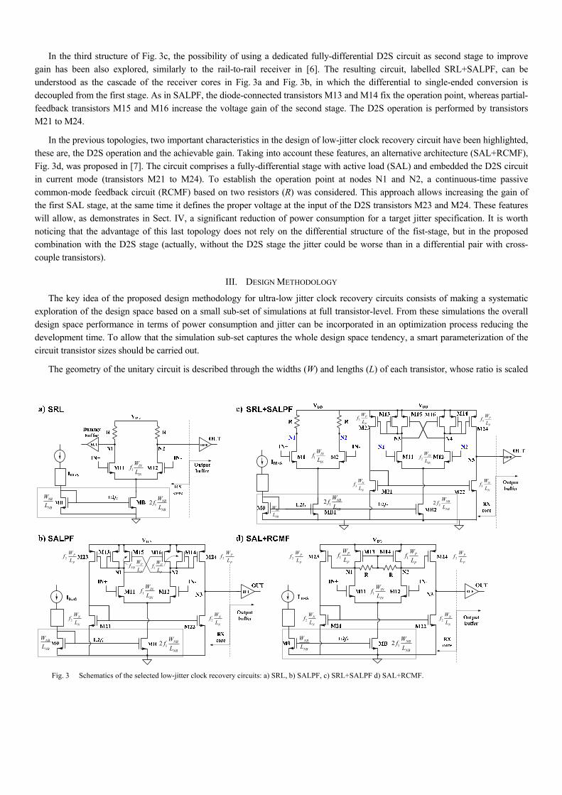
In the third structure of Fig. 3c, the possibility of using a dedicated fully-differential D2S circuit as second stage to improve gain has been also explored, similarly to the rail-to-rail receiver in [6]. The resulting circuit, labelled SRL+SALPF, can be understood as the cascade of the receiver cores in Fig. 3a and Fig. 3b, in which the differential to single-ended conversion is decoupled from the first stage. As in SALPF, the diode-connected transistors M13 and M14 fix the operation point, whereas partial-feedback transistors M15 and M16 increase the voltage gain of the second stage. The D2S operation is performed by transistors M21 to M24.
In the previous topologies, two important characteristics in the design of low-jitter clock recovery circuit have been highlighted, these are, the D2S operation and the achievable gain. Taking into account these features, an alternative architecture (SAL+RCMF), Fig. 3d, was proposed in [7]. The circuit comprises a fully-differential stage with active load (SAL) and embedded the D2S circuit in current mode (transistors M21 to M24). To establish the operation point at nodes N1 and N2, a continuous-time passive common-mode feedback circuit (RCMF) based on two resistors (R) was considered. This approach allows increasing the gain of the first SAL stage, at the same time it defines the proper voltage at the input of the D2S transistors M23 and M24. These features will allow, as demonstrates in Sect. IV, a significant reduction of power consumption for a target jitter specification. It is worth noticing that the advantage of this last topology does not rely on the differential structure of the fist-stage, but in the proposed combination with the D2S stage (actually, without the D2S stage the jitter could be worse than in a differential pair with cross-couple transistors).
III. DESIGN METHODOLOGY
The key idea of the proposed design methodology for ultra-low jitter clock recovery circuits consists of making a systematic exploration of the design space based on a small sub-set of simulations at full transistor-level. From these simulations the overall design space performance in terms of power consumption and jitter can be incorporated in an optimization process reducing the development time. To allow that the simulation sub-set captures the whole design space tendency, a smart parameterization of the circuit transistor sizes should be carried out.
The geometry of the unitary circuit is described through the widths (W) and lengths (L) of each transistor, whose ratio is scaled
3P
P
Wf
L
12 NB
NB
Wf
L
NB
NB
W
L
PFB
P
Wf
L 1P
P
Wf
L
2P
P
Wf
L
2N
N
Wf
L
12 NB
NB
Wf
L
1IN
IN
Wf
L
NB
NB
W
L
1IN
IN
Wf
L
2P
P
Wf
L
2N
N
Wf
L
2IN
IN
Wf
L1
IN
IN
Wf
L
NB
NB
W
L
12 NB
NB
Wf
L 22 NB
NB
Wf
L
3N
N
Wf
L 3N
N
Wf
L
3P
P
Wf
L
12 NB
NB
Wf
L
1IN
IN
Wf
L
1P
P
Wf
L
NB
NB
W
L
1P
P
Wf
L2P
P
Wf
L 2P
P
Wf
L
2N
N
Wf
L 2N
N
Wf
L
Fig. 3 Schematics of the selected low-jitter clock recovery circuits: a) SRL, b) SALPF, c) SRL+SALPF d) SAL+RCMF.
by its corresponding multiplicity factor {f1,f2,...,fi,..}, where i is an integer number which identifies the different current branches in the circuit starting from the first stage up to the final digital buffer following the signal flow, as shown in Fig. 3. To assure a correct scaling between stages, the coefficients fi for a specific current branch are defined relatively to the previous branches in the queue. To give an intuitive view of the physical meaning of this parameterization, let us focus on the SAL+RCMF topology of Fig. 3d. For
this structure, a relative scale factor (2) between its two constitutive branches has been considered: 1) the first stage (biased by MB)
and 2) the D2S stage (M21 to M24), in the form, f2=2·f1. This relative definition of scale factors will allow, as described later, that
the specification (power and jitter) dependences on the design parameters have smooth behaviors, at the same time that, it minimizes the selection of candidate solutions that are suitable from a practical point view during the optimization phase.
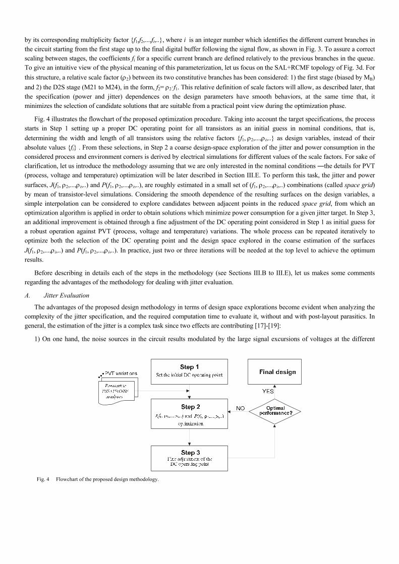
Fig. 4 illustrates the flowchart of the proposed optimization procedure. Taking into account the target specifications, the process starts in Step 1 setting up a proper DC operating point for all transistors as an initial guess in nominal conditions, that is,
determining the width and length of all transistors using the relative factors {f1,2,...,i,..} as design variables, instead of their
absolute values {fi} . From these selections, in Step 2 a coarse design-space exploration of the jitter and power consumption in the considered process and environment corners is derived by electrical simulations for different values of the scale factors. For sake of clarification, let us introduce the methodology assuming that we are only interested in the nominal conditions ―the details for PVT (process, voltage and temperature) optimization will be later described in Section III.E. To perform this task, the jitter and power
surfaces, J(f1,2,...,i,..) and P(f1,2,...,i,..), are roughly estimated in a small set of (f1,2,...,i,..) combinations (called space grid)
by mean of transistor-level simulations. Considering the smooth dependence of the resulting surfaces on the design variables, a simple interpolation can be considered to explore candidates between adjacent points in the reduced space grid, from which an optimization algorithm is applied in order to obtain solutions which minimize power consumption for a given jitter target. In Step 3, an additional improvement is obtained through a fine adjustment of the DC operating point considered in Step 1 as initial guess for a robust operation against PVT (process, voltage and temperature) variations. The whole process can be repeated iteratively to optimize both the selection of the DC operating point and the design space explored in the coarse estimation of the surfaces
J(f1,2,...,i,..) and P(f1,2,...,i,..). In practice, just two or three iterations will be needed at the top level to achieve the optimum
results.
Before describing in details each of the steps in the methodology (see Sections III.B to III.E), let us makes some comments regarding the advantages of the methodology for dealing with jitter evaluation.
A. Jitter Evaluation
The advantages of the proposed design methodology in terms of design space explorations become evident when analyzing the complexity of the jitter specification, and the required computation time to evaluate it, without and with post-layout parasitics. In general, the estimation of the jitter is a complex task since two effects are contributing [17]-[19]:
1) On one hand, the noise sources in the circuit results modulated by the large signal excursions of voltages at the different
Fig. 4 Flowchart of the proposed design methodology.
nodes. In consequence, if we try to estimate jitter from basic AC or OP simulations, optimist values will be derived. For instance, in a fully differential implementation as the one in Fig. 3a, current source transistor MB has little impact on the total output noise, since it contributes at a common-mode node. However, in large signal regimen, this transistor becomes one of the most relevant one. This effect is well known in oscillators [20].
2) On the other hand, due to the discrete nature of jitter, the effect of all noise sources in the system is just relevant on the edges of the clock. However, these sources will result sampled by the clock event itself, causing that high-frequency contributions are down-converter to the region of interest, up to half the sampling frequency (Nyquist’s bandwidth), increasing total jitter budget. This down sampling process rises the complexity of the evaluation, since significant harmonics of the clock effectively contribute (in our case, up to 31-th harmonics are considered; above this frequency, the contribution is marginal).
Taking into account the previous characteristics, the estimation of jitter by simulations is performed in two phases. First, a Periodic Steady-State analysis (PSS) with a realistic input stimulus is run to determine the quiescent situation in large signal regimen. From it a Periodic Noise analysis (PNOISE) is executed to evaluate the sampled noise density function, which once integrated in the Nyquist’s bandwidth provides the jitter standard deviation and peak-to-peak values. The number of such simulations is not negligible even for circuits with relative small number of transistors, as in the examples of Fig. 3. To give an idea of the computation time, more than six minutes are required at the schematic–level without parasitics for each point in the space grid―simulations were carried out in a Fujitsu CX400 linux server using 24 dedicated cores in a Intel Xeon E5-2630v2 6C/12T 2.60MHz 15MB, 128GB DDR3-1600 at 2GHz. The situation is even worst when dealing with post-layout parasitic simulations (around fifty minutes per case), making evident the need for a smart exploration of the design space which reduces the number of design candidate evaluations.
In the following two sub-sections (III.B-III.D), additional information of each step in the optimization process of Fig. 4 is given. In Section III.E, the whole design process and extension to dealing with process and environment variations are detailed using the topology in Fig. 3d as demonstrator.
B. Step 1: initial quiescent point
The starting point in the methodology is the selection of the polarization conditions for all transistors in the circuit in the nominal situation (typical process and environment conditions for an input signal at half the voltage range VDD/2, as usual to provide maximum input excursion). By polarization conditions, it is understood the definition of the overdrive voltages (|vOD|=|VGS|–|VTH|) for a given bias current. With the proposed parameterization, a significant reduction of the independent design variables is achieved, since the aspect ratios between transistors in current mirrors are relative to the previous branch and the current through differential input pairs are half the current of the bias transistor. The specific selection of the initial polarization conditions is not critical in the methodology, since it will be later optimized (see details in Section III.D).
As an initial guess of the operating point for correct analog operation, the following criteria are considered: 1) to bias all transistors in saturation region of strong inversion, 2) to assure that DC voltages of the critical internal nodes (for instance, N1, N2 and N3 in the topology of Fig. 3d) are between 80% and 120% of VDD/2 to provide enough excursion margins, 3) for differential input pairs, such as M11 and M12 in Fig. 3d, to consider an overdrive voltage around 150mV, 4) to set transistor lengths in differential pairs to low values so that the speed performance of the circuit is not impaired due to high capacitances, and 5) for the NMOS current sources of differential pairs, to use relative big length (above 2µm), since these transistors contribute significantly to the total jitter budget.
C. Step 2: scale factors variations
Once the DC operating point is set, the major improvements in the performance are achieved by adjusting properly the transistor scale factors. This task consists of studying how the jitter and power performance change when f1 and ρi are modified. As mentioned before, large signal simulations (PSS and PNOISE, respectively) instead of small signal (linear) analysis must be used to calculate jitter by transistor-level simulations. In the proposed approach the jitter estimations can be performed in an efficient
manner in terms of computation time using scale factors {f1,2,...,i,..} as design variables. By this parameterization, the power and
jitter surfaces J(f1,2,...,i,..) and P(f1,2,...,i,..), will show a smooth dependence on the design variables (f1,2,...,i,..) allowing a
simple interpolation to robustly explore new candidates between points in the space grid. The design optimization can be hence
formulated as a minimization process which reduces the power consumption for a given maximum value of the jitter performance, as state below:
int 1 1 2 1 1 2 2
int 1 0
Minimize ( ,..., ,...) in = ( , ,..., ...) [ , ] [ , ] ... [ , ] ...
Subject to: ( ,..., ,...)i i L U L U iL iU
i
P f f f f
J f J
(4)
where Pint(f1,2,...,i,..) and Jint(f1,2,...,i,..) are linear-interpolated surfaces of the simulated dataset of the power consumption and
the jitter performance, J0 is the maximum allowable jitter, and is the variation region.
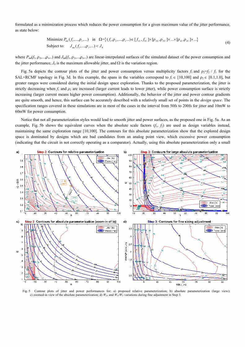
Fig. 5a depicts the contour plots of the jitter and power consumption versus multiplicity factors f1 and ρ2=f2 / f1 for the
SAL+RCMF topology in Fig. 3d. In this example, the spans in the variables correspond to f1 [10,100] and ρ2 [0.1,1.0], but
greater ranges were considered during the initial design space exploration. Thanks to the proposed parameterization, the jitter is strictly decreasing when f1 and ρ2 are increased (larger current leads to lower jitter), while power consumption surface is strictly increasing (larger current means higher power consumption). Additionally, the behavior of the jitter and power contour gradients are quite smooth, and hence, this surface can be accurately described with a relatively small set of points in the design space. The specification ranges covered in these simulations are in most of the cases in the interval from 50fs to 200fs for jitter and 10mW to 60mW for power consumption.
Notice that not all parameterization styles would lead to smooth jitter and power surfaces, as the proposed one in Fig. 5a. As an example, Fig. 5b shows the equivalent curves when the absolute scale factors (f1, f2) are used as design variables instead, maintaining the same exploration range [10,100]. The contours for this absolute parameterization show that the explored design space is dominated by designs which are bad candidates from an analog point view, which excessive power consumption (indicating that the circuit in not correctly operating as a comparator). Actually, using this absolute parameterization only a small
Fig. 5 Contour plots of jitter and power performances for: a) proposed relative parameterization; b) absolute parameterization (large view);c) zoomed-in view of the absolute parameterization; d) WIN and WN/WP variations during fine adjustment in Step 3.

region at the bottom (f2<10) of the explored design space is really interesting for design. Even if the design space is restricted to this region as shown in Fig. 5c, the jitter and power regions that ensures correct operation are less smoother than for the proposed parametrization in Fig. 5a), while reducing the explored region in terms of transistor size, and hence, incrementing the chance that good candidates are not covered.
D. Step 3: fine adjustment of the DC operating point
In this step of the methodology a fine adjustment of the transistor operating point (OP) in nominal conditions is carried out considering as input the selected candidate from the previous phase. This allows additional improvements in performance and robustness against PVT variations introducing slight modifications of the polarization conditions to optimize the initial selection in Step 1. Once the new operating point has been selected, it is mandatory to verify that biasing conditions described in step 1 are still fulfilled for robust analog operation. Further iterations from Step 1 to Step 3 could be done in order to obtain more competitive results. In practice, 2 or 3 iterations are enough to achieve convergence of the whole process.
As an example for the implementation of Fig. 3d, Fig. 5d shows the jitter and power contour curves using the width of the input pair (WIN) and the ration between the PMOS and NMOS current source widths (r = WN /WP ) as parameters. For this topology, the optimum response for a jitter specification below 70fs is found in the central region, which corresponds to WIN values between 10µm and 25µm and r between 0.5 and 2.5. In this area, power is minimized for the lowest values of r and WIN.
E. Case study
In this subsection the validation results at full transistor-level of the proposed methodology are presented using the topology of Fig. 3d for illustration purpose, without lack of generality. For the application of the methodology to other clock receiver architectures, such as the other ones in Fig. 3, please refer to the comparison study of Section IV. To show the trade-off between power consumption and jitter within a specific process and across technologies nodes, results for two different commercial foundries are herein presented: 1) initially, simulations for 1.8V 0.18µm CMOS are shown; 2) at the end, results for a 1.2V 90nm are reported.
For these experiments, the clock recovery circuit (Rx) has been excited with a fully differential sinusoidal input with 0.9V common mode (VDD/2). Two diodes, which limit the amplitude at 400mVpp of each input, have been considered to protect the circuit [2]. The bias reference is IBIAS = 100µA, which implies that total current through transistor MB is 2f1·IBIAS. Jitter has been calculated in Spectre within Cadence Design FrameWork environment from PSS-PNOISE analyses considering a clock frequency of 100MHz and integrating within whole Nyquist’s band from 100 Hz to 50MHz. Additional practical details of the methodologies steps can be found next:
Step 1: attending to the design criteria in Section III.B, the following initial values of widths and lengths of the transistors were considered: WIN=5µm, LIN=0.18µm, WN=2µm, LN= 0.5µm, WP=2µm, LP=0.18µm, WNB=16µm, LNB=2µm. This sizing ensures that all transistors remain in saturation region of strong inversion. In a first survey, a coarse sweep (ITER1) of the design variables with
spans of f1 [10,200], ρ2 [0.1,2.0] and grid size of 10x10 points, were considered. After identification of the regions where the
best candidates were located, a finer sweep (ITER2) of the design space with f1 [10,100] and ρ2 [0.1,1.0] with the same grid
size was considered in a second inspection, which is depicted in Fig. 5a. In ITER2, which was the last refinement in this step, the length of transistor MB was modified from the original LNB=2µm to the final LNB=5µm, maintaining the aspect ratio (i.e. doing WNB=40µm), to reduce the jitter noise, since the current source was identified as one of the most relevant contributors to the total jitter budget. Table 1 summarizes the normalized transistor sizes (Wx/Lx) and the scale factors (f1, ρ2) for some points in the space grid; in particular, the center point of the explored region in each survey: (100, 1.0) in ITER1 and (55, 0.5) in ITER2. The relationship between the normalized and the total transistor width is given by the scale factors themselves according to the proposed relative parameterization in the second column of the table. Finally, the values after OP optimization (in Step 3 of ITER2) are also included. The table also shows the corresponding overdrive voltages (|vOD|) for the quiescent operation point. Notice that all values are above 100mV in magnitude.
Step 2: as described in Section III.C, the jitter and power surfaces, J(f1,2) and P(f1, 2) can be approximated by interpolating the
results of parametric sweep analyses. In general, a grid of N values for each parameter, f1 and 2, uniformly distributed between
the design boundaries is considered. As these surfaces are relatively flat and smooth, a simple linear 2-D approach for the

simulation data interpolation has been used to obtain the jitter and power functions, Jint (f1,2) and Pint (f1, 2). The optimization
problem in (4) has been formulated as a constrained nonlinear multivariable minimization in MATLABTM. Fig. 5a illustrates before (orange point), and after (green point) the step 2 is applied.
Table 1. Details of SAL+RCMF circuit in steps 1 and 3 of the proposed methodology.
Transistor Sizing
Step 1 (ITER1)
Step 1 (ITER2)
Step 3(ITER2)
(f1,2) Wx/Lx
(µm/ µm) |vOD| (mV) (f1,2)
Wx/Lx
(µm/ µm) |vOD| (mV) (f1,2)
Wx/Lx
(µm/ µm) |vOD|(mV)
MB 2f1· (WNB/LNB)
(100,1)
16/2.0 287
(55,0.5)
40/5.0 287
(50,0.3)
40/5.0 288 M0 WNB/LNB 16/2.0 285 40/5.0 286 40/5.0 286
M23/M24 f2·(WP/LP) 2/0.18 413 2/0.18 414 2/0.18 421 M13/M14 f1·(WP/LP) 2/0.18 413 2/0.18 414 2/0.18 421 M21/M22 f2·(WN/LN) 2/0.50 372 2/0.50 370 2.4/0.50 347 M11/M12 f1·(WIN/LIN) 5/0.18 157 5/0.18 157 15/0.18 111
J = 60.01fs ; P = 56.85mW J = 60.27fs ; P = 29.56mW J = 67.8fs ; P = 23.9mW
The red dashed curve in Fig. 6a shows the initial pareto-optimum power/jitter front without OP fine adjustment. Six different designs with target J0 jitter from 70fs to 120fs in steps of 10fs, labelled #1 to #6, are considered to illustrate the trade-off between
power consumption and maximum allowable jitter. For each point, the optimum values of the design parameter (f1, 2) are depicted.
These values typically falls between two adjacent points in the explored space design, ITER2: 100 points, in
={(f1, 2 ) [10,100]×[0.1,1.0]}, however, due to the smooth surface property, non-significant errors between estimated
(interpolated) and actual transistor-level simulations corresponding to each point are achieved. Actually, the maximum deviations between the interpolated and the measured values by electrical simulation are lower than 4.0fs and 0.2mW, respectively.
Step 3: according to the design rules inferred from Fig. 5d, in the fine adjustment step the transistor width in the differential pair WIN was increased to 15µm, whereas r was set to 1.2 with WP =2µm, for an optimum performance. Following this strategy, an average reduction of 35% in power consumption for the same jitter target was obtained, as the difference between the red dashed and blue continuous curve in Fig. 6a shows. To clearly identify the starting and ending states in the curves, each pair of design with
common scale factors (f1, 2) uses the same marker shape in both curves. The distinction between designs in a couple without and
with OP adjustment is just found on the normalized transistor sizes, as reported in Table 1.
As previously highlighted, optimum results typically falls between two adjacent points in the space grid. In Fig. 6b (bottom-left blue curves), a comparison between the estimated (by interpolation) and the actual simulated values by electrical simulation at transistor-level are depicted. Again, the maximum deviations for jitter and power are lower than 4.0fs and 0.2mW, respectively,
Fig. 6 a) Improvement of the power performance in step 3 regarding step 2; b) comparison between results obtained from Spectre simulations and the proposed estimations (by interpolation) for 90nm and 180nm nodes.

being the interpolated version always in worst conditions.
The achieved accuracy versus Spectre makes the proposed methodology suitable for agile exploration of the design space in different technology nodes since a very short time is required for a systematic evaluation. Actually, in the context of [16] for the development of a 1.8V 2Vpp 80dB-SNDR 100Msps Pipeline ADC, this approach was used as one of the metrics for the selection of the technology. In Fig. 6b (top-right green curves), the equivalents results of the designs in a 90nm CMOS process is included as an example. In this case, the use of thick oxide transistors biased at 1.8V were imposed by the ADC input range (2Vpp), justifying the worse performance than in the 180nm process (due their lower mobility and greater parasitics). Based on this behavior, the decision on favor of the 180nm CMOS process was clearer to our application ―in that follows, this node will be implicitly assumed.
Robustness considerations: to conclude the design verification, the problematic associated to PVT variations at transistor-level are addressed next. For these experiments five corners with different bias and temperature conditions have been selected, labelled: Typical, FastN/FastP, FastN/SlowP, SlowN/FastP, SlowN/SlowP. To do that, two different situations are distinguished: 1) we will show the impact of PVT variations on a design which have been optimized in typical conditions, analyzing the performance degradations, 2) we will illustrate how PVT variation can be incorporated in the design flow.
Fig. 7a shows the impact of PVT variations on the optimized designs of Fig. 6a (#1 to #6) without PVT optimization. To clearly identify the correspondence between specific designs, the same maker shape is maintained. Note that SlowN/SlowP corner solutions are shifted left upward (high-jitter and low-power) regarding the typical case. On the other hand, FastN/FastP points move right downward (low-jitter and high-power). Although from all these results, we can always try to find a specific design which satisfies the requirements in all considered corners, this approach could lead to non-optimum solutions, since pareto-optimal front is not any more evaluated.
To avoid sub-optimal final selection, the information of PVT variations must be incorporated in the optimization design flow itself. In our methodology, this information has been straightforward dealt by simple evaluating the PVT variations during the design space characterization in Step 2. Following this approach, the jitter and power surfaces just need to incorporate an extra dummy-variable, c, for each corner, in the form: Pint(f1, ρi, c) and Jint(f1, ρi, c), while the optimization problem in (4) is reformulated to show explicitly the corners dependence on this way: minimizing the highest power consumption between all corners for each point of variation region and for a given maximum value of the jitter performance,
int 1 1 2
int 1 0
Minimize max ( ,..., ,..., ) in *= , ,...,
Subject to: ( ,..., ,..., )
i Pc
i
P f c c c c
J f c J
(5)
where Pint(f1,2,...,i,..,c) and Jint(f1,2,...,i,.. ,c) are linear-interpolated surfaces of the simulated dataset of the power consumption
and the jitter performance per corner c from the all considered P corners. With this modification, the flowchart of the proposed
Typical / 27ºC / V =1.8VDD
FastN/FastP / -50ºC / V =1.89VDD
FastN/SlowP / 27ºC / V =1.80VDD
SlowN/FastP / 27ºC / V =1.80VDD
SlowN/SlowP / 75ºC / V =1.71VDD
Typical / 27ºC / V =1.8VDD
FastN/FastP / -50ºC / V =1.89VDD
FastN/SlowP / 27ºC / V =1.80VDD
SlowN/FastP / 27ºC / V =1.80VDD
SlowN/SlowP / 75ºC / V =1.71VDD
Fig. 7 Jitter vs. power consumption plot for corner scenarios: a) characterization of the designs in Fig. 6a (same circuit design); b) designing for the same values of J0 in each corner (different transistor sizes per corner).

methodology in Fig. 4 can be maintained.
Fig. 7b shows the pareto-optimal front for our case of study using the previous optimization problem. Results for the different corners when each case is design to obtain a certain value of J0 are provided. Again, the correspondence between curves is identified with the same marker. When compared with Fig. 7a, the more relevant observation is that there is almost null dispersion in the vertical axis, since the jitter specification has been imposed for power optimization. Regarding the horizontal axis, the power consumption shows lower dispersion for the upper limit of jitter (J0 = 120fs), around 3mW between the FastN/FastP and the SlowN/SlowP corners, while for low jitter values the dispersion increases up to 15mW for J0 = 70fs. This behavior is consequent with the expected response for analog circuits, i.e. the lower the specifications are, the more chance for satisfying them in all corners, while for specifications close to the technological limits, the difficulties increase, and it could eventually lead to an unfeasible design or the need of relaxing requirements in the design phase for some specific corner (for instance the SlowN/SlowP). In circuit realization at technology limits, this is usually addressed introducing a spinning phase during experimental test to classify samples attending to its maximum performance (for instance, operation frequency in processor).
IV. COMPARISON STUDY
In this section, the proposed methodology is applied to the rest of topologies in Fig. 3 for showing the generality of the method and performance comparison. Two sets of experiments have been carried out in order to compare the studied clock recovery circuits at the target clock input frequency of 100MHz. In the first set of simulations, the topologies have been sized for optimal performance of the product between the jitter and the power consumption (PJP) as classical figure of merit in this scope. Fig. 8a shows power vs. jitter plots for each topology. Although theoretically an explicit distinction on the rising and falling edges at the output of the receiver should be performed, since all structures in Fig. 3 are no symmetric by construction, simulations results do not show significant differences ―in figure, output rising edge measurements are report (falling edge performance results are slightly better). From the point of view of the PJP metric, it can be inferred that the best trade-off between power consumption and jitter performances is achieved for the SAL+RCMF clock recovery circuit (Fig. 3d) with a jitter and power consumption of around 80fs and 30mW at 100MHz input frequency. Note that the estimated jitter at 100MHz is basically determined by the slope of the reconstructed clock edges. For this design the rise and fall times are always below 100ps, and therefore, it can operate at frequency well above 100MHz up to near the GHz as shown in Fig. 9 (above GHz, the design is still functional but the transistor electrical models are questionable). As expected for a circuit in which the broadband noise sources dominate, the jitter decreases with clock frequency [21], being relatively constant above 500MHz at around 30fs level. An intuitive view of this behavior is achieved considering that the clock signal (clk) is in general a linear combination of its harmonics, and that the receiver has a finite bandwidth. Therefore, the more clock frequency is, the less the harmonics which contribute to the noise, and the lower the jitter.
The second set of simulations evaluates power consumption for a fixed output jitter J0 of 200fs in typical conditions, again on the rising edge. The relative high value of specification J0 has been deliberately selected to give chance to most of the topologies of
Fig. 8 Comparison study at transistor-level: a) power consumption versus jitter plot; values of the Power Jitter Product (PJP) performance are also indicated for each topology; b) power consumption for a jitter goal of 200fs for a set of corners scenarios.
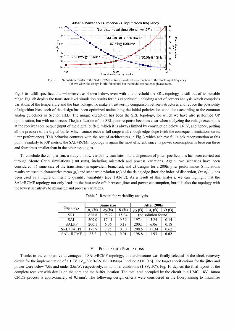
Fig. 3 to fulfill specifications ―however, as shown below, even with this threshold the SRL topology is still out of its suitable range. Fig. 8b depicts the transistor-level simulation results for this experiment, including a set of corners analysis which comprises variations of the temperature and the bias voltage. To make a trustworthy comparison between structures and reduce the possibility of algorithm bias, each of the design has been optimized maintaining the initial polarization conditions according to the common analog guidelines in Section III.B. The unique exception has been the SRL topology, for which we have also performed OP optimization, but with no success. The justification of the SRL poor response becomes clear when analyzing the voltage excursions at the receiver core output (input of the digital buffer), which it is always limited by construction below 1.61V, and hence, putting all the pressure of the digital buffer which cannot recover full range with enough edge slope (with the consequent limitations on its jitter performance). This behavior contrasts with the rest of architectures in Fig. 3 which achieve full clock reconstruction at this point. Similarly to PJP metric, the SAL+RCMF topology is again the most efficient, since its power consumption is between three and four times smaller than in the other topologies.
To conclude the comparison, a study on how variability translates into a dispersion of jitter specifications has been carried out through Monte Carlo simulations (100 runs), including mismatch and process variations. Again, two scenarios have been considered: 1) same size of the transistors (in equivalent branches), and 2) designs for a 200fs jitter performance. Simulations results are used to characterize mean (µJ) and standard deviation (σJ) of the rising edge jitter; the index of dispersion, D= σJ
2/µJ, has been used as a figure of merit to quantify variability (see Table 2). As a result of this analysis, we can highlight that the SAL+RCMF topology not only leads to the best trade-offs between jitter and power consumption, but it is also the topology with the lowest sensitivity to mismatch and process variations.
Table 2. Results for variability analysis.
Topology Same size Jitter 200fs
µJ (fs) σJ (fs) D (fs) µJ (fs) σJ (fs) D (fs) SRL 628.8 98.22 15.34 (no solution found) SAL 509.0 17.41 0.59 197.4 5.24 0.14
SALPF 200.1 6.06 0.18 200.1 6.06 0.18 SRL+SALPF 175.9 7.25 0.30 208.5 11.34 0.62 SAL+RCMF 83.2 0.94 0.01 198.8 1.93 0.02
V. POST-LAYOUT SIMULATIONS
Thanks to the competitive advantages of SAL+RCMF topology, this architecture was finally selected in the clock recovery circuit for the implementation of a 1.8V 2Vpp 80dB-SNDR 100Msps Pipeline ADC [16]. The target specifications for the jitter and power were below 75fs and under 25mW, respectively, in nominal conditions (1.8V, 50º). Fig. 10 depicts the final layout of the complete receiver with details on the core and the buffer location. The total area occupied by the circuit in a UMC 1.8V 180nm CMOS process is approximately of 0.1mm2. The following design criteria were considered in the floorplanning to maximize
Fig. 9 Simulation results of the SAL+RCMF at transistor-level as a function of the clock input frequency
(above GHz, the design is still functional but the model are not enough accurate).
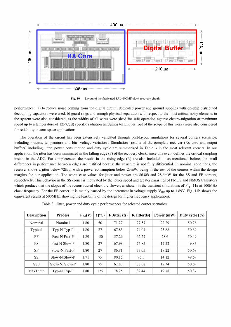
performance: a) to reduce noise coming from the digital circuit, dedicated power and ground supplies with on-chip distributed decoupling capacitors were used, b) guard rings and enough physical separation with respect to the most critical noisy elements in the system were also considered, c) the widths of all wires were sized for safe operation against electro-migration at maximum speed up to a temperature of 125ºC, d) specific radiation hardening techniques (out of the scope of this work) were also considered for reliability in aero-space applications.
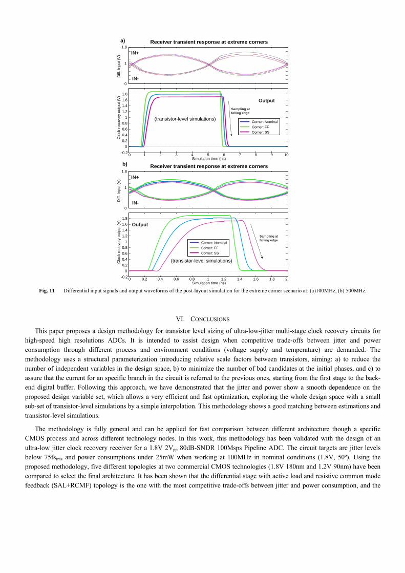
The operation of the circuit has been extensively validated through post-layout simulations for several corners scenarios, including process, temperature and bias voltage variations. Simulations results of the complete receiver (Rx core and output buffers) including jitter, power consumption and duty cycle are summarized in Table 3 in the most relevant corners. In our application, the jitter has been minimized in the falling edge (F) of the recovery clock, since this event defines the critical sampling instant in the ADC. For completeness, the results in the rising edge (R) are also included ― as mentioned before, the small differences in performance between edges are justified because the structure is not fully differential. In nominal conditions, the receiver shows a jitter below 72fsrms with a power consumption below 23mW, being in the rest of the corners within the design margins for our application. The worst case values for jitter and power are 86.8fs and 28.6mW for the SS and FF corners, respectively. This behavior in the SS corner is motivated by the lower speed and greater parasitics of PMOS and NMOS transistors which produce that the slopes of the reconstructed clock are slower, as shown in the transient simulations of Fig. 11a at 100MHz clock frequency. For the FF corner, it is mainly caused by the increment in voltage supply VDD up to 1.89V. Fig. 11b shows the equivalent results at 500MHz, showing the feasibility of the design for higher frequency applications.
Table 3. Jitter, power and duty cycle performances for selected corner scenarios
Description Process VDD(V) t (ºC) F Jitter (fs) R Jitter(fs) Power (mW) Duty cycle (%)
Nominal Nominal 1.80 50 71.27 77.57 22.29 50.76
Typical Typ-N Typ-P 1.80 27 67.83 74.04 23.88 50.69
FF Fast-N Fast-P 1.89 -50 57.26 62.27 28.6 50.49
FS Fast-N Slow-P 1.80 27 67.98 75.85 17.52 49.83
SF Slow-N Fast-P 1.80 27 86.81 73.05 18.22 50.68
SS Slow-N Slow-P 1.71 75 80.15 96.5 14.12 49.69
SS0 Slow-N, Slow-P 1.80 75 67.83 88.68 17.34 50.69
MaxTemp Typ-N Typ-P 1.80 125 78.25 82.44 19.78 50.87
Fig. 10 Layout of the fabricated SAL+RCMF clock recovery circuit.
VI. CONCLUSIONS
This paper proposes a design methodology for transistor level sizing of ultra-low-jitter multi-stage clock recovery circuits for high-speed high resolutions ADCs. It is intended to assist design when competitive trade-offs between jitter and power consumption through different process and environment conditions (voltage supply and temperature) are demanded. The methodology uses a structural parameterization introducing relative scale factors between transistors, aiming: a) to reduce the number of independent variables in the design space, b) to minimize the number of bad candidates at the initial phases, and c) to assure that the current for an specific branch in the circuit is referred to the previous ones, starting from the first stage to the back-end digital buffer. Following this approach, we have demonstrated that the jitter and power show a smooth dependence on the proposed design variable set, which allows a very efficient and fast optimization, exploring the whole design space with a small sub-set of transistor-level simulations by a simple interpolation. This methodology shows a good matching between estimations and transistor-level simulations.
The methodology is fully general and can be applied for fast comparison between different architecture though a specific CMOS process and across different technology nodes. In this work, this methodology has been validated with the design of an ultra-low jitter clock recovery receiver for a 1.8V 2Vpp 80dB-SNDR 100Msps Pipeline ADC. The circuit targets are jitter levels below 75fsrms and power consumptions under 25mW when working at 100MHz in nominal conditions (1.8V, 50º). Using the proposed methodology, five different topologies at two commercial CMOS technologies (1.8V 180nm and 1.2V 90nm) have been compared to select the final architecture. It has been shown that the differential stage with active load and resistive common mode feedback (SAL+RCMF) topology is the one with the most competitive trade-offs between jitter and power consumption, and the
0 1 2 3 4 5 6 7 8 9 10-0.2
0
0.2
0.4
0.6
0.8
1
1.2
1.4
1.6
1.8
Clo
ck r
ecov
ery
outp
ut (
V)
Corner: Nominal
Corner: FF
Corner: SS
(transistor-level simulations)
0
1
1.8Receiver transient response at extreme corners
Diff
. In
put (
V) IN+
IN-
Output
Simulation time (ns)
Sampling at falling edge
0 0.2 0.4 0.6 0.8 1 1.2 1.4 1.6 1.8 2-0.2
0
0.2
0.4
0.6
0.8
1
1.2
1.4
1.6
1.8
Clo
ck r
ecov
ery
out
put (
V)
Corner: Nominal
Corner: FF
Corner: SS
(transistor-level simulations)
0
1
1.8Receiver transient response at extreme corners
Diff
. Inp
ut (
V) IN+
IN-
Output
Simulation time (ns)
Sampling at falling edge
a)
b)
Fig. 11 Differential input signals and output waveforms of the post-layout simulation for the extreme corner scenario at: (a)100MHz, (b) 500MHz.
lowest sensitivity to PVT variations and mismatch. Post-layout simulation results of SAL+RCMF circuit implemented in a UMC 1.8V 180nm CMOS process shows its suitability for sub-100fs jitter applications with a robust operation against process and environment changes.
ACKNOWLEDGEMENTS
This work was supported in part by the Spanish Government projects TEC2015-68448-R cofinanced by the European FEDER program, and by the European Space Agency (ESA) contract: 4000108445-13-NL-RA “ADC 16bits”.
REFERENCES
[1] H.-S Lee and C. G. Sodini, "Analog-to-Digital Converters: Digitizing the Analog World," in Proceedings of the IEEE, vol. 96, no. 2, pp. 323-334, Feb. 2008.
[2] B. Brannon, “Sampled Systems and the Effects of Clock Phase Noise and Jitter”, Analog Devices Application Note, AN-756, 2004. [3] A. Zanchi and F. Tsay, "A 16-bit 65-MS/s 3.3-V pipeline ADC core in SiGe BiCMOS with 78-dB SNR and 180-fs jitter," in IEEE Journal of Solid-State
Circuits, vol. 40, no. 6, pp. 1225-1237, June 2005. [4] L. Cheng, H. Yang, L. Luo and J. Ren, "Analysis and design of low-jitter clock driver for wideband ADC," Solid-State and Integrated Circuit Technology
(ICSICT), 2010 10th IEEE International Conference on, Shanghai, 2010, pp. 515-517. [5] Y. Unekawa et al., "A 5 Gb/s 8/spl times/8 ATM switch element CMOS LSI supporting five quality-of-service classes with 200 MHz LVDS
interface," Solid-State Circuits Conference, 1996. Digest of Technical Papers. 42nd ISSCC., 1996 IEEE International, San Francisco, CA, USA, 1996, pp. 118-119.
[6] A. Boni, A. Pierazzi and D. Vecchi, "LVDS I/O interface for Gb/s-per-pin operation in 0.35-μm CMOS," in IEEE Journal of Solid-State Circuits, vol. 36, no. 4, pp. 706-711, Apr 2001.
[7] J Núñez, A. J. Ginés, E. J. Peralías and A. Rueda, "Low-jitter differential clock driver circuits for high-performance high-resolution ADCs," Design of Circuits and Integrated Systems (DCIS), 2015 Conference on, Estoril, 2015, pp. 1-4.
[8] G. Alpaydin, S. Balkir and G. Dundar, "An evolutionary approach to automatic synthesis of high-performance analog integrated circuits," in IEEE Transactions on Evolutionary Computation, vol. 7, no. 3, pp. 240-252, June 2003.
[9] M. Barros, J. Guilherme, N. Horta, “Analog circuits optimization based on evolutionary computation techniques”, Integration, the VLSI Journal, vol. 43, issue 1, January 2010, pp. 136-155.
[10] K. Deb, A. Pratap, S. Agarwal and T. Meyarivan, "A fast and elitist multiobjective genetic algorithm: NSGA-II," in IEEE Transactions on Evolutionary Computation, vol. 6, no. 2, pp. 182-197, Apr 2002.
[11] Medeiro, Fernando, Pérez-Verdú, Belén, Rodríguez-Vázquez, Angel, “Top-Down Design of High-Performance Sigma-Delta Modulators”, Dordrecht. Kluwer Academic Publishers, 1998, ISBN 0-7923-8352-4.
[12] B. Liu, F. V. Fernandez and G. G. E. Gielen, "Efficient and Accurate Statistical Analog Yield Optimization and Variation-Aware Circuit Sizing Based on Computational Intelligence Techniques," in IEEE Transactions on Computer-Aided Design of Integrated Circuits and Systems, vol. 30, no. 6, pp. 793-805, June 2011.
[13] J. Goes, J. C. Vital and J. Franca, “Systematic Design for Optimisation of Pipelined ADCs,” Kluwer Academic Publisher, 2001. ISBN 0792372913. [14] J. Núñez, A. J. Ginés, E. J. Peralías and A. Rueda, "An approach to the design of low-jitter differential clock recovery circuits for high performance
ADCs," Circuits & Systems (LASCAS), 2015 IEEE 6th Latin American Symposium on, Montevideo, 2015, pp. 1-4. [15] IEEE Standards, “IEEE standard for terminology and test methods for analog-to-digital converters,” IEEE Std 1241-2000, 2001. [16] European Space Agency (ESA) contract: 4000108445-13-NL-RA “ADC 16bits”. [17] A. Demir, A. Sangiovanni-Vincentelli. Analysis and Simulation of Noise in Nonlinear Electronic Circuits and Systems. Kluwer Academic Publishers, 1997,
ISBN-10: 0792380371. [18] J. Phillips and K. Kundert, "Noise in mixers, oscillators, samplers, and logic an introduction to cyclostationary noise," Custom Integrated Circuits
Conference, 2000. CICC. Proceedings of the IEEE 2000, Orlando, FL, 2000, pp. 431-438. [19] K. Kunder, “Predicting the Phase Noise and Jitter of PLL-Based Frequency Synthesizers”, v.4i, October 2015, available at http://www.designers-
guide.org/analysis. [20] E. Hegazi, H. Sjoland, A. A. Abidi, "A filtering technique to lower LC oscillator phase noise," IEEE Journal of Solid-State Circuits, vol. 36, no. 12, pp.
1921-1930, Dec 2001. [21] Maxim Integrated Products: Application Note 3631, “Random Noise Contribution to Timing Jitter—Theory and Practice”, available at
http://www.maximintegrated.com/an3631.