impact of synaptic device variations on pattern...
TRANSCRIPT

1SCientifiC REPORTS | (2018) 8:2638 | DOI:10.1038/s41598-018-21057-x
www.nature.com/scientificreports
Impact of Synaptic Device Variations on Pattern Recognition Accuracy in a Hardware Neural NetworkSungho Kim1, Meehyun Lim2, Yeamin Kim3, Hee-Dong Kim1 & Sung-Jin Choi 3
Neuromorphic systems (hardware neural networks) derive inspiration from biological neural systems and are expected to be a computing breakthrough beyond conventional von Neumann architecture. Interestingly, in neuromorphic systems, the processing and storing of information can be performed simultaneously by modulating the connection strength of a synaptic device (i.e., synaptic weight). Previously investigated synaptic devices can emulate the functionality of biological synapses successfully by utilizing various nano-electronic phenomena; however, the impact of intrinsic synaptic device variability on the system performance has not yet been studied. Here, we perform a device-to-system level simulation of different synaptic device variation parameters in a designed neuromorphic system that has the potential for unsupervised learning and pattern recognition. The effects of variations in parameters such as the weight modulation nonlinearity (NL), the minimum-maximum weight (Gmin and Gmax), and the weight update margin (ΔG) on the pattern recognition accuracy are analyzed quantitatively. These simulation results can provide guidelines for the continued design and optimization of a synaptic device for realizing a functional large-scale neuromorphic computing system.
The mammalian neocortex offers extremely energy-efficient information processing performance in tasks such as pattern recognition with a power consumption of only 10–20 watts1. By mimicking both the functional and struc-tural advantages of this biological neural system, the recent development of power-efficient computing systems, i.e., neuromorphic systems (hardware neural networks)2, has been expected to offer a promising breakthrough for applications, ranging from mobile platforms3 to artificial intelligence operations4, where power consumption is a concern.
A unique feature of neuromorphic systems is efficient parallel data processing, where the processing of infor-mation can be performed by modulating the connection strength of synapses (referred to as the synaptic weight)5. This synaptic weight can be modulated by either potentiating or depressing neural spikes (pulses) from pre- and post-synaptic neurons, following appropriate learning rules, such as spike-timing-dependent plasticity (STDP)6. Therefore, a key element in the neuromorphic system is the implementation of an ideal synaptic device that can emulate the functionality of biological synapses.
To date, various nano-electronic devices have successfully reproduced a specific learning rule of biological synapses through their internal analog conductance states that can be modulated intentionally with an applied pulse’s timing or level7–15. Moreover, the potential of ultralow energy consumption per synaptic operation16, as well as the possibility of realizing three-dimensional integration17, have shown the promising feasibility of large-scale neuromorphic system implementation in the near future. However, the sustainability of such devices is still in doubt due to the variability issue that is common to all nano-electronic devices18–20. The physical mecha-nism of the conductance modulation in most prospective synaptic devices, which is typically a random process in an atomic-level change based on electro/thermo-dynamics21, is responsible for an unavoidable device-to-device22 variation. In particular, the effect of device variations on the neuromorphic system performance, e.g. pattern
1Department of Electrical Engineering, Sejong University, Seoul, 05006, Korea. 2Mechatronics R&D Center, Samsung Electronics, Gyonggi-do, 18448, Korea. 3School of Electrical Engineering, Kookmin University, Seoul, 02707, Korea. Sungho Kim, Meehyun Lim and Yeamin Kim contributed equally to this work. Correspondence and requests for materials should be addressed to S.-J.C. (email: [email protected])
Received: 2 November 2017
Accepted: 29 January 2018
Published: xx xx xxxx
OPEN
www.nature.com/scientificreports/
2SCientifiC REPORTS | (2018) 8:2638 | DOI:10.1038/s41598-018-21057-x
recognition accuracy, has not been analyzed quantitatively23–28, which leads to a bottleneck in the continuing design and optimization of synaptic devices and the entire system.
In this study, a device-to-system level simulation presents quantitative results in terms of the neuromorphic system performance depending on different device variation parameters, where the discussed system has the potential for unsupervised online learning and consequent image classification for MNIST handwritten digits. The effect of the synaptic device variations in the weight modulation nonlinearity (NL), the minimum-maximum weight (Gmin and Gmax), and the weight update margin (ΔG) on the pattern recognition accuracy is analyzed. These simulation results provide a design guideline for the specifications of the synaptic device needed for more reliable system operation. Here, note that our analysis is only limited to the neuromorphic system that are capable of online learning. Since the system operated by offline-learning is consisted of only synaptic device network and dos not require peripheral circuits, the effects of different device variation parameters to the system performance is easily predictable and well-discussed by previous studies23–25. In contrast, the comprehensive study for the effects of device variation to the system performance with online-learning has been missing29–32, thus our study aims the quantitative analysis to understand how the pattern recognition accuracy of the existing STDP-based online-learning system affected by device variation parameters.
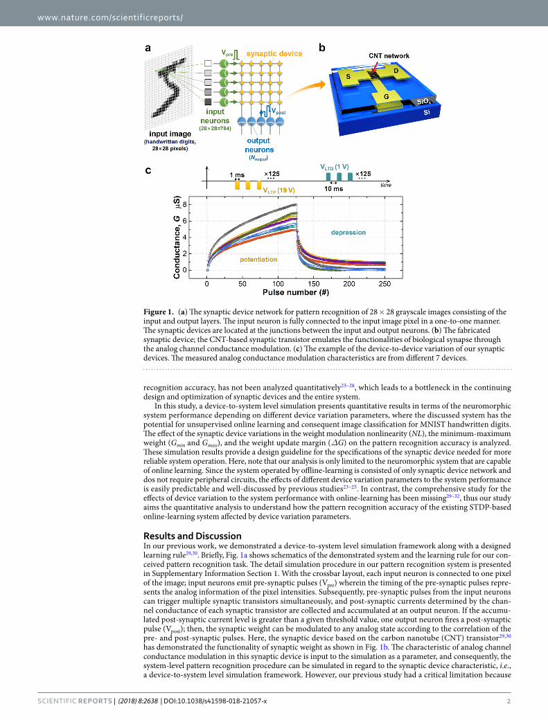
Results and DiscussionIn our previous work, we demonstrated a device-to-system level simulation framework along with a designed learning rule29,30. Briefly, Fig. 1a shows schematics of the demonstrated system and the learning rule for our con-ceived pattern recognition task. The detail simulation procedure in our pattern recognition system is presented in Supplementary Information Section 1. With the crossbar layout, each input neuron is connected to one pixel of the image; input neurons emit pre-synaptic pulses (Vpre) wherein the timing of the pre-synaptic pulses repre-sents the analog information of the pixel intensities. Subsequently, pre-synaptic pulses from the input neurons can trigger multiple synaptic transistors simultaneously, and post-synaptic currents determined by the chan-nel conductance of each synaptic transistor are collected and accumulated at an output neuron. If the accumu-lated post-synaptic current level is greater than a given threshold value, one output neuron fires a post-synaptic pulse (Vpost); then, the synaptic weight can be modulated to any analog state according to the correlation of the pre- and post-synaptic pulses. Here, the synaptic device based on the carbon nanotube (CNT) transistor29,30 has demonstrated the functionality of synaptic weight as shown in Fig. 1b. The characteristic of analog channel conductance modulation in this synaptic device is input to the simulation as a parameter, and consequently, the system-level pattern recognition procedure can be simulated in regard to the synaptic device characteristic, i.e., a device-to-system level simulation framework. However, our previous study had a critical limitation because
Figure 1. (a) The synaptic device network for pattern recognition of 28 × 28 grayscale images consisting of the input and output layers. The input neuron is fully connected to the input image pixel in a one-to-one manner. The synaptic devices are located at the junctions between the input and output neurons. (b) The fabricated synaptic device; the CNT-based synaptic transistor emulates the functionalities of biological synapse through the analog channel conductance modulation. (c) The example of the device-to-device variation of our synaptic devices. The measured analog conductance modulation characteristics are from different 7 devices.
www.nature.com/scientificreports/
3SCientifiC REPORTS | (2018) 8:2638 | DOI:10.1038/s41598-018-21057-x
the effect of synaptic device variations was ignored. Despite the intrinsic device-to-device variation of the syn-aptic devices as shown in Fig. 1c, the simulation was performed by reflecting only one device characteristic and assuming all synaptic devices had the equivalent characteristic29,30 (the discussions about the origin of variation and working principle in our synaptic device are presented in the Supplementary Information Section 2 and 3, respectively). Since this approach has been common in other studies for simulation simplicity31–33, an accurate quantitative analysis of such a neuromorphic system has not yet been conducted. Therefore, in this study, we investigate how different synaptic device variations affect the pattern recognition accuracy of the system by using our simulation and considering the device-to-device variation.
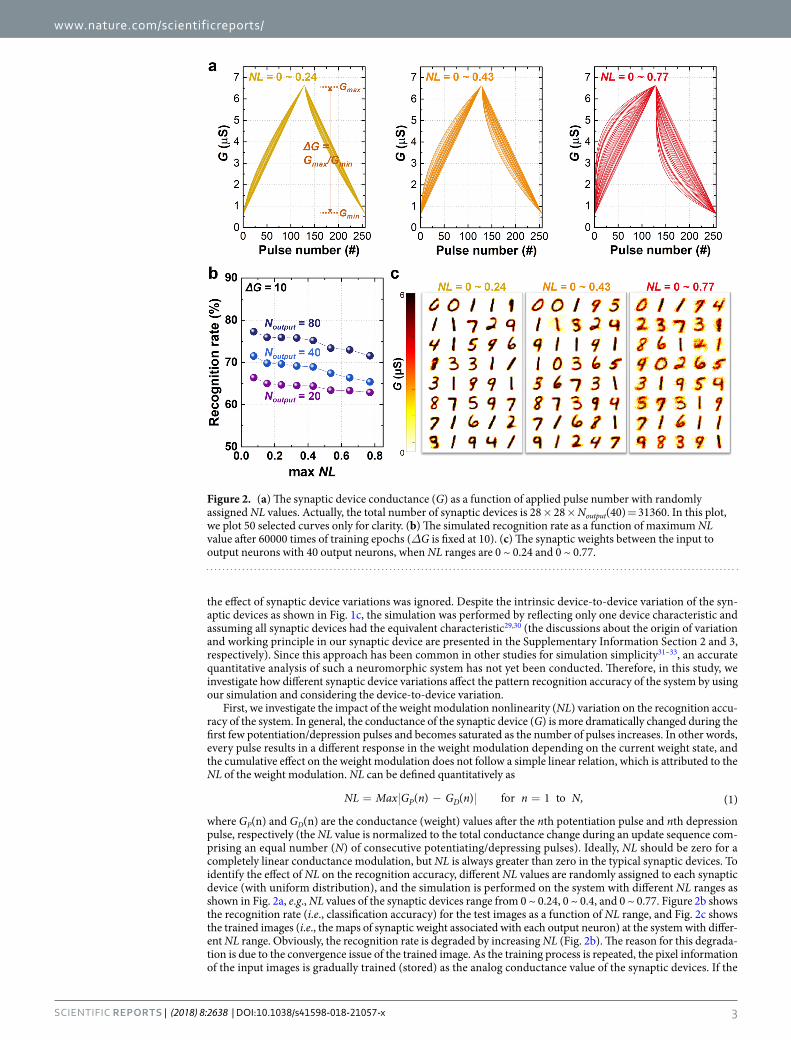
First, we investigate the impact of the weight modulation nonlinearity (NL) variation on the recognition accu-racy of the system. In general, the conductance of the synaptic device (G) is more dramatically changed during the first few potentiation/depression pulses and becomes saturated as the number of pulses increases. In other words, every pulse results in a different response in the weight modulation depending on the current weight state, and the cumulative effect on the weight modulation does not follow a simple linear relation, which is attributed to the NL of the weight modulation. NL can be defined quantitatively as
= − =NL Max G n G n n N,( ) ( ) for 1 to (1)P D
where GP(n) and GD(n) are the conductance (weight) values after the nth potentiation pulse and nth depression pulse, respectively (the NL value is normalized to the total conductance change during an update sequence com-prising an equal number (N) of consecutive potentiating/depressing pulses). Ideally, NL should be zero for a completely linear conductance modulation, but NL is always greater than zero in the typical synaptic devices. To identify the effect of NL on the recognition accuracy, different NL values are randomly assigned to each synaptic device (with uniform distribution), and the simulation is performed on the system with different NL ranges as shown in Fig. 2a, e.g., NL values of the synaptic devices range from 0 ~ 0.24, 0 ~ 0.4, and 0 ~ 0.77. Figure 2b shows the recognition rate (i.e., classification accuracy) for the test images as a function of NL range, and Fig. 2c shows the trained images (i.e., the maps of synaptic weight associated with each output neuron) at the system with differ-ent NL range. Obviously, the recognition rate is degraded by increasing NL (Fig. 2b). The reason for this degrada-tion is due to the convergence issue of the trained image. As the training process is repeated, the pixel information of the input images is gradually trained (stored) as the analog conductance value of the synaptic devices. If the
Figure 2. (a) The synaptic device conductance (G) as a function of applied pulse number with randomly assigned NL values. Actually, the total number of synaptic devices is 28 × 28 × Noutput(40) = 31360. In this plot, we plot 50 selected curves only for clarity. (b) The simulated recognition rate as a function of maximum NL value after 60000 times of training epochs (ΔG is fixed at 10). (c) The synaptic weights between the input to output neurons with 40 output neurons, when NL ranges are 0 ~ 0.24 and 0 ~ 0.77.
www.nature.com/scientificreports/
4SCientifiC REPORTS | (2018) 8:2638 | DOI:10.1038/s41598-018-21057-x
NL value is increased, the conductance change of the synaptic device occurs abruptly, causing difficulty in the convergence of the conductance into a final stable value. Consequently, irregular pixel values (noise-like) occur in the background of the trained image as shown in Fig. 2c, which results in the degradation of the recognition rate. However, it should be noted that the effect of NL is not critical in maintaining the recognition rate; the rec-ognition rate reduction by NL is only 6% from the best to the worst cases (when Noutput = 40, Fig. 2b). Therefore, it can be concluded that the nonlinearity of the weight modulation at the synaptic device, i.e., NL, is not critical to the recognition rate of the system. This implies that further synaptic device study should be devoted more to improving characteristics other than NL, unlike other previous efforts to improve NL24,34.
Note that this conclusion is the opposite of the results in previous studies, where increasing NL degrade the recognition rate obviously24,34. For example, in previous work based on conventional backpropagation learning rule with neural network architecture24, because all synaptic weights (along with the function of the perceptron) in the whole neural network contribute to the learning process, a precise adjustment of all synaptic weights is necessarily required. In contrast, in our system, since only the synaptic weight associated with one fired output neuron involves the learning process, an iterative modulation of the synaptic weight is more important than the precise adjustment. Consequently, this difference indicates that the required specification of the synaptic device is not determinative, but it depends on what learning rules and architecture are used to construct the system. Only studies to reduce NL value34–38 are not always the best way to optimize the synaptic device performance.
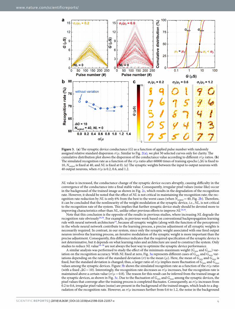
A similar analysis was performed to study the effect of the minimum-maximum weight (Gmin and Gmax) var-iation on the recognition accuracy. With NL fixed at zero, Fig. 3a represents different cases of Gmin and Gmax var-iations depending on the ratio of the standard deviation (σ) to the mean (μ). Here, the mean of Gmin and Gmax is fixed, but the standard deviation is changed; thus, a larger ratio of σ/μ implies more fluctuation of Gmin and Gmax values among the synaptic devices. Figure 3b shows the simulated recognition rate as a function of the σ/μ ratio (with a fixed ΔG = 10). Interestingly, the recognition rate decreases as σ/μ increases, but the recognition rate is maintained above a certain value (σ/μ = 0.8). The reason for this result can be inferred from the trained image at the synaptic devices, as shown in Fig. 3c. Due to the fluctuation of Gmin and Gmax among the synaptic devices, the pixel values that converge after the training process is completed fluctuates. Consequently, as σ/μ increases from 0.2 to 0.6, irregular pixel values (noise) are present in the background of the trained images, which leads to a deg-radation of the recognition rate. However, as σ/μ increases further from 0.6 to 1.2, the noise in the background
Figure 3. (a) The synaptic device conductance (G) as a function of applied pulse number with randomly assigned relative standard dispersion σ/μ. Similar to Fig. 2(a), we plot 50 selected curves only for clarity. The cumulative distribution plot shows the dispersion of the conductance value according to different σ/μ ratios. (b) The simulated recognition rate as a function of the σ/μ ratio after 60000 times of training epochs (ΔG is fixed to 10, Noutput is fixed at 40, and NL is fixed at 0). (c) The synaptic weights between the input to output neurons with 40 output neurons, when σ/μ is 0.2, 0.6, and 1.2.
www.nature.com/scientificreports/
5SCientifiC REPORTS | (2018) 8:2638 | DOI:10.1038/s41598-018-21057-x
can be compensated by the effect of increasing the pixel value of the main image. In other words, the pixel value difference between the main image and the background becomes larger by increasing σ/μ, which makes the image more distinct and easier to distinguish. Therefore, the variation of the minimum-maximum weight at the synaptic devices, i.e., Gmin and Gmax, determines the recognition rate through the correlation of the increase of irregular background noise and the image distinguishability.
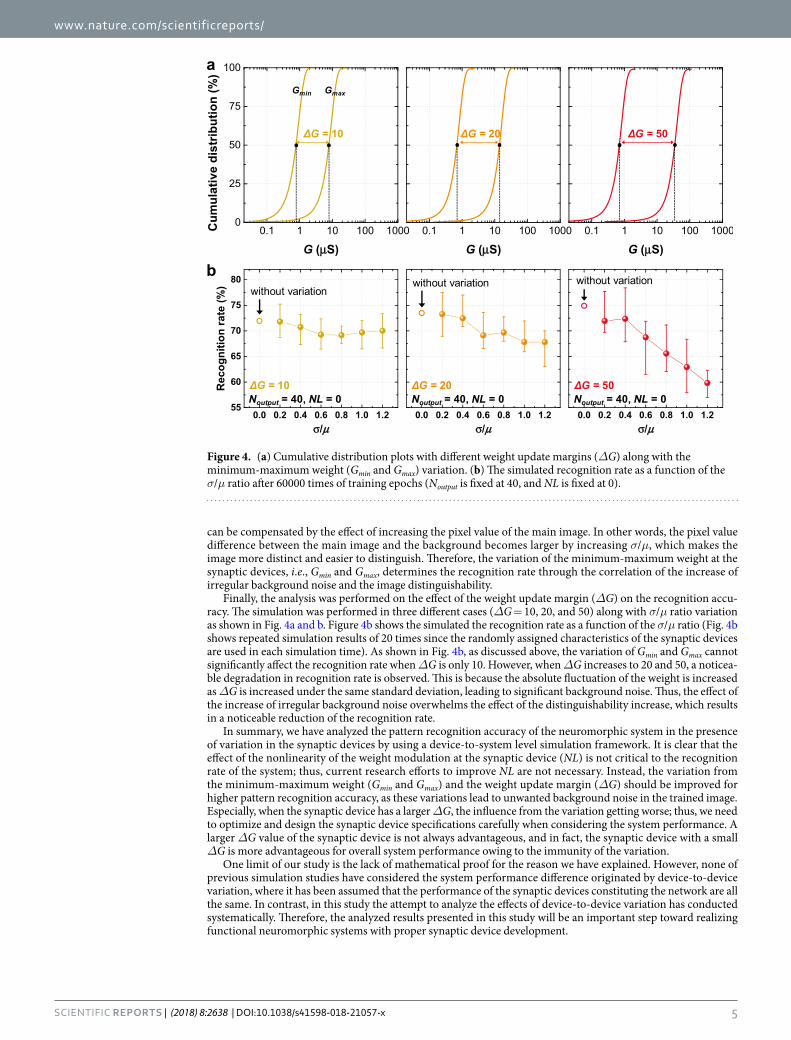
Finally, the analysis was performed on the effect of the weight update margin (ΔG) on the recognition accu-racy. The simulation was performed in three different cases (ΔG = 10, 20, and 50) along with σ/μ ratio variation as shown in Fig. 4a and b. Figure 4b shows the simulated the recognition rate as a function of the σ/μ ratio (Fig. 4b shows repeated simulation results of 20 times since the randomly assigned characteristics of the synaptic devices are used in each simulation time). As shown in Fig. 4b, as discussed above, the variation of Gmin and Gmax cannot significantly affect the recognition rate when ΔG is only 10. However, when ΔG increases to 20 and 50, a noticea-ble degradation in recognition rate is observed. This is because the absolute fluctuation of the weight is increased as ΔG is increased under the same standard deviation, leading to significant background noise. Thus, the effect of the increase of irregular background noise overwhelms the effect of the distinguishability increase, which results in a noticeable reduction of the recognition rate.
In summary, we have analyzed the pattern recognition accuracy of the neuromorphic system in the presence of variation in the synaptic devices by using a device-to-system level simulation framework. It is clear that the effect of the nonlinearity of the weight modulation at the synaptic device (NL) is not critical to the recognition rate of the system; thus, current research efforts to improve NL are not necessary. Instead, the variation from the minimum-maximum weight (Gmin and Gmax) and the weight update margin (ΔG) should be improved for higher pattern recognition accuracy, as these variations lead to unwanted background noise in the trained image. Especially, when the synaptic device has a larger ΔG, the influence from the variation getting worse; thus, we need to optimize and design the synaptic device specifications carefully when considering the system performance. A larger ΔG value of the synaptic device is not always advantageous, and in fact, the synaptic device with a small ΔG is more advantageous for overall system performance owing to the immunity of the variation.
One limit of our study is the lack of mathematical proof for the reason we have explained. However, none of previous simulation studies have considered the system performance difference originated by device-to-device variation, where it has been assumed that the performance of the synaptic devices constituting the network are all the same. In contrast, in this study the attempt to analyze the effects of device-to-device variation has conducted systematically. Therefore, the analyzed results presented in this study will be an important step toward realizing functional neuromorphic systems with proper synaptic device development.
Figure 4. (a) Cumulative distribution plots with different weight update margins (ΔG) along with the minimum-maximum weight (Gmin and Gmax) variation. (b) The simulated recognition rate as a function of the σ/μ ratio after 60000 times of training epochs (Noutput is fixed at 40, and NL is fixed at 0).
www.nature.com/scientificreports/
6SCientifiC REPORTS | (2018) 8:2638 | DOI:10.1038/s41598-018-21057-x
MethodsFabrication of carbon nanotube-based synaptic transistors. Carbon nanotube (CNT) synaptic tran-sistors were initially fabricated on highly p-doped rigid silicon substrates with a thermally grown 50-nm-thick SiO2 layer. We used the local back-gate structure for efficient local modulation of the channels in the CNT transis-tors. To form the local back-gate, the palladium (Pd) layer was first deposited and subsequently patterned using evaporation and a lift-off process. Next, a 50-nm-thick SiOx layer, 10-nm-thick Au layer, and 20-nm-thick SiOx layer were deposited sequentially. The thin Au layer served as a floating gate for charge storage. Then, the top surface of the SiOx layer was functionalized with a 0.1 g/mL poly-L-lysine solution to form an amine-terminated layer, which acted as an effective adhesion layer for the deposition of the CNTs. Subsequently, the CNT network channel was formed by immersing the chip into a 0.01 mg/mL 99%-semiconducting CNT solution (NanoIntegris, Inc.) for several hours followed by a thorough rinse with isopropanol and DI water. Subsequently, the source/drain electrodes consisting of Ti and Pd layers (each 2 nm and 40 nm, respectively) were deposited and patterned using conventional thermal evaporation and a lift-off process, respectively. Finally, additional photolithography and oxygen plasma steps were conducted to remove unwanted electrical paths, which isolated the devices from one another.
References 1. Javed, F. et al. Brain and high metabolic rate organ mass: Contributions to resting energy expenditure beyond fat-free mass. Am. J.
Clin. Nutr. 91, 907–912 (2010). 2. Mead, C. Neuromorphic Electronic Systems. Proc. IEEE 78, 1629–1636 (1990). 3. Etienne-Cummings, R., Mehta, S., Philipp, R. & Gruev, V. Neuromorphic Vision Systems for Mobile Applications. in IEEE Custom
Integrated Circuits Conference 2006 531–534, https://doi.org/10.1109/CICC.2006.320906 (IEEE, 2006). 4. Esser, S. K. et al. Convolutional networks for fast, energy-efficient neuromorphic computing. Proc. Natl. Acad. Sci. USA 113,
11441–11446 (2016). 5. Abbott, L. F. & Regehr, W. G. Synaptic computation. Nature 431, 796–803 (2004). 6. Bi, G. Q. & Poo, M. M. Synaptic modifications in cultured hippocampal neurons: dependence on spike timing, synaptic strength,
and postsynaptic cell type. J. Neurosci. 18, 10464–10472 (1998). 7. Zamarreño-Ramos, C. et al. On spike-timing-dependent-plasticity, memristive devices, and building a self-learning visual cortex.
Front. Neurosci. 5, 26 (2011). 8. Serrano-Gotarredona, T., Masquelier, T., Prodromakis, T., Indiveri, G. & Linares-Barranco, B. STDP and STDP variations with
memristors for spiking neuromorphic learning systems. Front. Neurosci. 7, 2 (2013). 9. Jo, S. H. et al. Nanoscale memristor device as synapse in neuromorphic systems. Nano Lett. 10, 1297–1301 (2010). 10. Yu, S., Wu, Y., Jeyasingh, R., Kuzum, D. & Wong, H. S. P. An electronic synapse device based on metal oxide resistive switching
memory for neuromorphic computation. IEEE Trans. Electron Devices 58, 2729–2737 (2011). 11. Kim, S. et al. Experimental demonstration of a second-order memristor and its ability to biorealistically implement synaptic
plasticity. Nano Lett. 15, 2203–2211 (2015). 12. Du, C., Ma, W., Chang, T., Sheridan, P. & Lu, W. D. Biorealistic Implementation of Synaptic Functions with Oxide Memristors
through Internal Ionic Dynamics. Adv. Funct. Mater. 25, 4290–4299 (2015). 13. Zhu, L. Q., Wan, C. J., Guo, L. Q., Shi, Y. & Wan, Q. Artificial synapse network on inorganic proton conductor for neuromorphic
systems. Nat. Commun. 5, 333–342 (2014). 14. Shi, J., Ha, S. D., Zhou, Y., Schoofs, F. & Ramanathan, S. A correlated nickelate synaptic transistor. Nat. Commun. 4, 84508 (2013). 15. Alibart, F. et al. An Organic Nanoparticle Transistor Behaving as a Biological Spiking Synapse. Adv. Funct. Mater. 20, 330–337
(2010). 16. Yu, S. et al. A neuromorphic visual system using RRAM synaptic devices with Sub-pJ energy and tolerance to variability:
Experimental characterization and large-scale modeling. In International Electron Devices Meeting 10.4.1–10.4.4, https://doi.org/10.1109/IEDM.2012.6479018 (IEEE, 2012).
17. Gao, B. et al. Ultra-Low-Energy Three-Dimensional Oxide-Based Electronic Synapses for Implementation of Robust High-Accuracy Neuromorphic Computation Systems. ACS Nano 8, 6998–7004 (2014).
18. Narayanan, P. et al. Parameter Variability in Nanoscale Fabrics: Bottom-Up Integrated Exploration. In IEEE 25th International Symposium on Defect and Fault Tolerance in VLSI Systems 24–31, https://doi.org/10.1109/DFT.2010.10 (IEEE, 2010).
19. Zhao, W., Querlioz, D., Klein, J.-O., Chabi, D. & Chappert, C. Nanodevice-based novel computing paradigms and the neuromorphic approach. In IEEE International Symposium on Circuits and Systems 2509–2512, https://doi.org/10.1109/ISCAS.2012.6271812 (IEEE, 2012).
20. Pouyan, P., Amat, E. & Rubio, A. Reliability challenges in design of memristive memories. In 5th European Workshop on CMOS Variability (VARI) 1–6, https://doi.org/10.1109/VARI.2014.6957074 (IEEE, 2014).
21. Ielmini, D. Modeling the universal set/reset characteristics of bipolar RRAM by field- and temperature-driven filament growth. IEEE Trans. Electron Devices 58, 4309–4317 (2011).
22. Kuzum, D., Yu, S. & Philip Wong, H.-S. Synaptic electronics: materials, devices and applications. Nanotechnology 24, 382001 (2013). 23. Park, S. et al. Neuromorphic speech systems using advanced ReRAM-based synapse. In Technical Digest - International Electron
Devices Meeting, IEDM 25.6.1–25.6.4, https://doi.org/10.1109/IEDM.2013.6724692 (IEEE, 2013). 24. Burr, G. W. et al. Experimental Demonstration and Tolerancing of a Large-Scale Neural Network (165 000 Synapses) Using Phase-
Change Memory as the Synaptic Weight Element. IEEE Trans. Electron Devices 62, 3498–3507 (2015). 25. Yu, S. et al. Scaling-up resistive synaptic arrays for neuro-inspired architecture: Challenges and prospect. In Technical Digest -
International Electron Devices Meeting, IEDM 17.3.1–17.3.4, https://doi.org/10.1109/IEDM.2015.7409718 (IEEE, 2015). 26. Sheridan, P. M. et al. Sparse coding with memristor networks. Nat. Nanotechnol. 12, 784–789 (2017). 27. Yao, P. et al. Face classification using electronic synapses. Nat. Commun. 8, 15199 (2017). 28. Wang, Z. et al. Memristors with diffusive dynamics as synaptic emulators for neuromorphic computing. Nat. Mater. 16, 101–108
(2016). 29. Kim, S., Yoon, J., Kim, H. D. & Choi, S. J. Carbon Nanotube Synaptic Transistor Network forPattern Recognition. ACS Appl. Mater.
Interfaces 7, 25479–25486 (2015). 30. Kim, S. et al. Pattern Recognition Using Carbon Nanotube Synaptic Transistors with an Adjustable Weight Update Protocol. ACS
Nano 11, 2814–2822 (2017). 31. Srinivasan, G., Sengupta, A. & Roy, K. Magnetic Tunnel Junction Based Long-Term Short-Term Stochastic Synapse for a Spiking
Neural Network with On-Chip STDP Learning. Sci. Rep. 6, 29545 (2016). 32. Wu, X., Saxena, V. & Zhu, K. Homogeneous Spiking Neuromorphic System for Real-WorldPattern Recognition. IEEE J. Emerg. Sel.
Top. Circuits Syst. 5, 254–266 (2015). 33. Diehl, P. U. & Cook, M. Unsupervised learning of digit recognition using spike-timing-dependent plasticity. Front. Comput.
Neurosci. 9, 99 (2015).
www.nature.com/scientificreports/
7SCientifiC REPORTS | (2018) 8:2638 | DOI:10.1038/s41598-018-21057-x
34. Wang, I.-T., Chang, C.-C., Chiu, L.-W., Chou, T. & Hou, T.-H. 3D Ta/TaOx/TiO2/Ti synaptic array and linearity tuning of weight update for hardware neural network applications. Nanotechnology 27, 365204 (2016).
35. Joshua Yang, J. et al. Engineering nonlinearity into memristors for passive crossbar applications. Appl. Phys. Lett. 100 (2012). 36. Wang, Z. et al. Engineering incremental resistive switching in TaO x based memristors for brain-inspired computing. Nanoscale 8,
14015–14022 (2016). 37. Bae, J.-H., Lim, S., Park, B.-G. & Lee, J.-H. High-Density and Near-Linear Synaptic Device Based on a Reconfigurable Gated
Schottky Diode. IEEE Electron Device Lett. 38, 1153–1156 (2017). 38. Wu, W. et al. Improving Analog Switching in HfO x -Based Resistive Memory With a Thermal Enhanced Layer. IEEE Electron Device
Lett. 38, 1019–1022 (2017).
AcknowledgementsThis research was supported by Nano·Material Technology Development Program (2016M3A7B4910430) and Basic Science Research Program (2016R1D1A1B03930162, 2016R1A2B4011366, and 2016R1A5A1012966) through the National Research Foundation (NRF) of Korea funded by the Ministry of Science, ICT and Future Planning. This work was partially supported by the Future Semiconductor Device Technology Development Program (Grant 10067739) funded by MOTIE (Ministry of Trade, Industry & Energy) and KSRC (Korea Semiconductor Research Consortium).
Author ContributionsThe manuscript was prepared by S.K., M.L., Y.K. and S.-J.C. Device fabrication and measurement were performed by S.K., Y.K. and simulation was performed by S.K., M.L., H.-D.K. and S.-J.C.
Additional InformationSupplementary information accompanies this paper at https://doi.org/10.1038/s41598-018-21057-x.Competing Interests: The authors declare no competing interests.Publisher's note: Springer Nature remains neutral with regard to jurisdictional claims in published maps and institutional affiliations.
Open Access This article is licensed under a Creative Commons Attribution 4.0 International License, which permits use, sharing, adaptation, distribution and reproduction in any medium or
format, as long as you give appropriate credit to the original author(s) and the source, provide a link to the Cre-ative Commons license, and indicate if changes were made. The images or other third party material in this article are included in the article’s Creative Commons license, unless indicated otherwise in a credit line to the material. If material is not included in the article’s Creative Commons license and your intended use is not per-mitted by statutory regulation or exceeds the permitted use, you will need to obtain permission directly from the copyright holder. To view a copy of this license, visit http://creativecommons.org/licenses/by/4.0/. © The Author(s) 2018