impact of fermi level pinning at polysilicon gate grain...
TRANSCRIPT
Impact of Fermi level pinning at polysilicon gate grain
boundaries on nano-MOSFET variability: A 3-D
simulation study
Andrew R. Brown, Gareth Roy and Asen Asenov
Device Modelling Group, Dept. of Electronics & Electrical Engineering
University of Glasgow
Glasgow, G12 8LT, United Kingdom
Abstract—In this paper we present a 3-D simulation study of
the effect of Fermi level pinning along polysilicon gate grain
boundaries on nano-MOSFET variability. Pinning of the
Fermi level results in variations between devices depending
on the random pattern of grain boundaries within the gate.
We present a coherent 3D simulation methodology
demonstrating the necessity of statistical simulations. As an
illustration of our approach, we have carried out a statistical
analysis of the variation in threshold voltage induced by
polysilicon grain boundaries for a 30 nm MOSFET.
I. INTRODUCTION
With the scaling of modern MOSFETs to deca-nanometre and nanometre dimensions, the intrinsic parameter variation introduced mainly by discreteness of charge and granularity of matter are become an increasing problem. Circuit and system performance and yield will be greatly affected at future generation technology nodes, and the analysis of such variations is vital for the continued advancement of the silicon industry. Various intrinsic sources if parameter fluctuations have been studied up to this point, including random discrete doping, line edge roughness and oxide thickness variation [1].
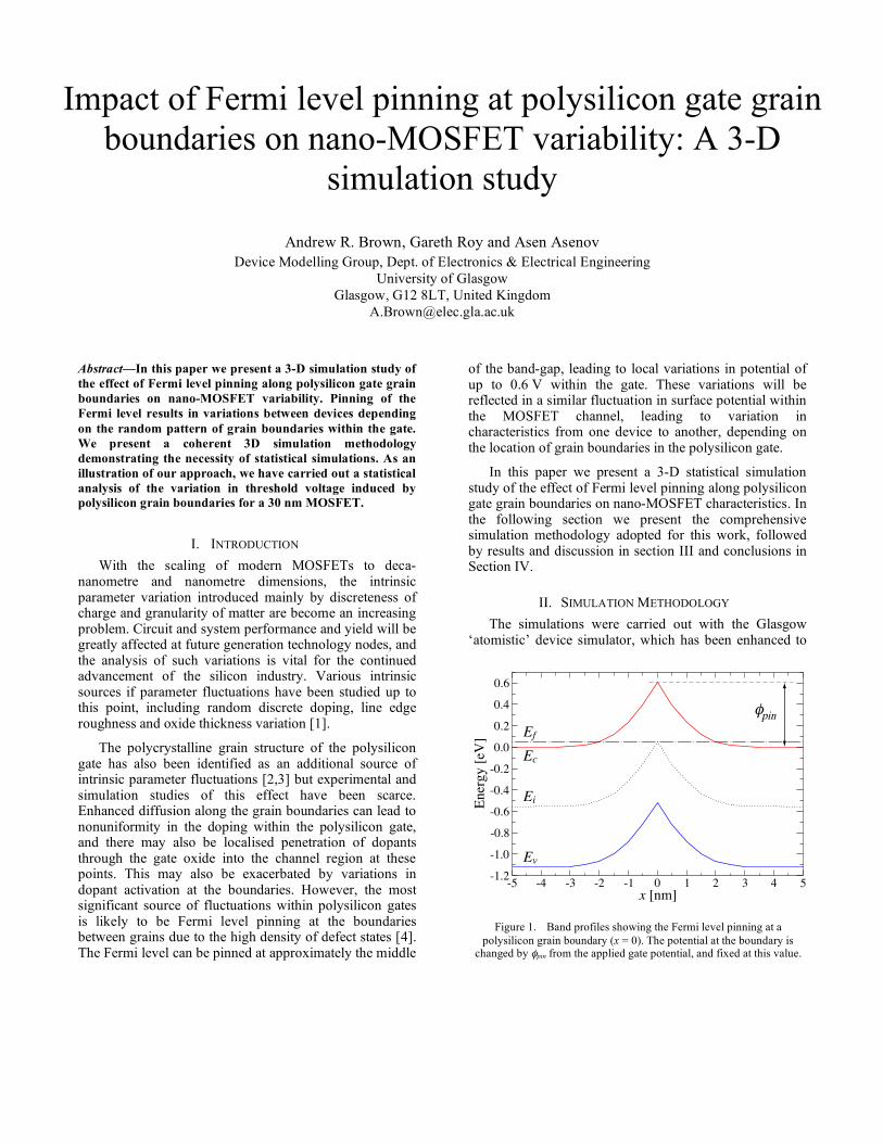
The polycrystalline grain structure of the polysilicon gate has also been identified as an additional source of intrinsic parameter fluctuations [2,3] but experimental and simulation studies of this effect have been scarce. Enhanced diffusion along the grain boundaries can lead to nonuniformity in the doping within the polysilicon gate, and there may also be localised penetration of dopants through the gate oxide into the channel region at these points. This may also be exacerbated by variations in dopant activation at the boundaries. However, the most significant source of fluctuations within polysilicon gates is likely to be Fermi level pinning at the boundaries between grains due to the high density of defect states [4]. The Fermi level can be pinned at approximately the middle
of the band-gap, leading to local variations in potential of up to 0.6 V within the gate. These variations will be reflected in a similar fluctuation in surface potential within the MOSFET channel, leading to variation in characteristics from one device to another, depending on the location of grain boundaries in the polysilicon gate.
In this paper we present a 3-D statistical simulation study of the effect of Fermi level pinning along polysilicon gate grain boundaries on nano-MOSFET characteristics. In the following section we present the comprehensive simulation methodology adopted for this work, followed by results and discussion in section III and conclusions in Section IV.
II. SIMULATION METHODOLOGY
The simulations were carried out with the Glasgow ‘atomistic’ device simulator, which has been enhanced to
-5 -4 -3 -2 -1 0 1 2 3 4 5x [nm]
-1.2
-1.0
-0.8
-0.6
-0.4
-0.2
0.0
0.2
0.4
0.6
Ene
rgy
[eV
] Ef
Ec
Ei
Ev
φpin
Figure 1. Band profiles showing the Fermi level pinning at a
polysilicon grain boundary (x = 0). The potential at the boundary is changed by pin from the applied gate potential, and fixed at this value.

include the pinning of the potential in the polysilicon gate along grain boundaries. This is a drift-diffusion simulator, using the density gradient method for quantum corrections. The applied gate potential in the polysilicon is modified by the pinning potential, pin, at the grain boundaries, such
that the Fermi level is at the pinning position. A one dimensional potential distribution in the direction normal to the grain boundary interface, and Fermi level pinning in the middle of the bandgap, are shown in Figure 1 for a polysilicon doping concentration of 10
20cm
-3.
In order to introduce a realistic random grain structure in the simulations, a large AFM image of polycrystalline silicon grains [5] has been used as a template (see Figure 2). The grain boundaries in this image were traced in black in Adobe Illustrator leaving the grains white, as shown in Figure 3. The polysilicon grain size distribution depends
strongly on the deposition and annealing conditions. In our example simulations the image was scaled so that the average grain diameter was approximately 40 nm, which has been observed experimentally [6]. A rasterised version of the template was saved in a format readable by the simulator.
The simulator imports a random (in both location and orientation) section of the grain template image that corresponds to the dimensions of the device. It pins the potential along any grain boundaries (defined by black pixels in the image) detected in the template section. The typical device dimensions simulated are much smaller than the dimensions of the template image, meaning we can extract a large number of completely independent grain patterns to use for the simulation of each different device in our statistical ensemble.
Figure 2. AFM image of polysilicon grains [5] used as a template for
our simulations
Figure 3. Image of polysilicon grain boundaries traced from the AFM image of Figure 2 using Adobe Illustrator.
0 0.2 0.4 0.6 0.8 1VG [V]
10-10
10-9
10-8
10-7
10-6
10-5
10-4
I D [
A/µ
m] No pinning
φpin = 0.1V
φpin = 0.2V
φpin = 0.3V
φpin = 0.4V
φpin = 0.5V
φpin = 0.6V (midgap)
S D
Figure 4. ID-VG characteristics for a 30 30 nm MOSFET with a single
polysilicon grain boundary orientated across the middle of the channel, as shown in the inset.
0 0.2 0.4 0.6 0.8 1VG [V]
10-10
10-9
10-8
10-7
10-6
10-5
10-4
I D [
A/µ
m] No pinning
φpin = 0.1V
φpin = 0.2V
φpin = 0.3V
φpin = 0.4V
φpin = 0.5V
φpin = 0.6V (midgap)
S D
Figure 5. ID-VG characteristics for a 30 30 nm MOSFET with a single
polysilicon grain boundary orientated along the channel in the centre, as shown in the inset.

III. RESULTS AND DISCUSSION
Previously published simulation studies have centred on 2-D simulations [4] or simulations with just a single grain boundary [2,7]. Initially we also present here simulations with a single grain boundary to demonstrate the potential impact of the Fermi level pinning in the polysilicon gate, and the grain boundary orientation, on the transistor characteristics. Figure 4 shows ID-VG
characteristics for a 30 30 nm MOSFET with Fermi level
pinning at a polysilicon grain boundary which extends across the middle of the channel, as demonstrated in the inset plan view of the MOSFET. The pinning position was varied from the unpinned Fermi level ( pin = 0V) to the
middle of the bandgap ( pin = 0.6V). The corresponding
shift of the threshold voltage, VT, gradually increases, up
to VT = 120 mV for the case of midgap pinning.
Figure 5 shows the results of similar simulations, however this time the polysilicon grain boundary is orientated along the direction of the channel, as shown in
the inset. The maximum threshold voltage shift, VT, in
this case is only 35 mV, and it is clear that the impact of the pinning is less.
The reason for this difference in VT becomes evident
from the map of the surface potential, which is shown in Figure 6 for the grain across the channel, and in Figure 7 for the grain along the channel. In the first case, the potential barrier between source and drain is increased by the presence of the grain boundary, and this extends right across the width of the device. In the second case, the increase in potential barrier is localised in the centre of the channel, allowing current to flow normally on either side. In this latter case, VT would also be dependent on the
width of the device simulated.
This dependence on grain boundary orientation demonstrates the necessity for a full three-dimensional analysis of the impact of the Fermi level pinning at polysilicon grain boundaries. Here we present statistical 3-D simulations investigating the fluctuations in device characteristics using a realistic polycrystalline grain pattern. An actual AFM image of polysilicon grains is used as a template, and introduced to the simulator as described in section II. The simulated device has 30 nm physical gate length, gate oxide thickness of 1 nm, a
uniform channel doping concentration NA = 3 1018
cm-3
and the polysilicon doping concentration is 1020
cm-3
.
Figure 8 shows the electrostatic potential within the
simulated 30 30 nm MOSFET with a particular pattern of
polysilicon grain boundaries which has been chosen randomly from the template image. The grain boundary
010
2030
4050
60
0
10
20
30
0
0.2
0.4
x [nm]y [nm]
Pote
ntia
l [V
]
Figure 6. Surface potential in the device from the case of Figure 4 with
grain boundary across the middle of the device (VG = 0 V, pin = 0.6V).
010
2030
x [nm]y [nm]
Pote
ntia
l [V
]
4050
60
0
10
20
30
0
0.2
0.4
Figure 7. Surface potential in the device from the case of Figure 5 with grain boundary along the channel in the centre (VG = 0 V, pin = 0.6V).
Figure 8. Electrostatic potential in a 30 30 nm MOSFET showing the
impact on the channel potential of Fermi level pinning at the polysilicon
grain boundaries. The location of the grain boundaries are shown in the
plane above the device.
pattern is shown in the plane above the MOSFET. The pinned gate potential, and associated depletion around the grain boundaries in the gate is reflected in a similar change in the surface potential in the channel of the MOSFET. As each simulated device has a different grain boundary pattern, the threshold voltage will vary from one device to another.
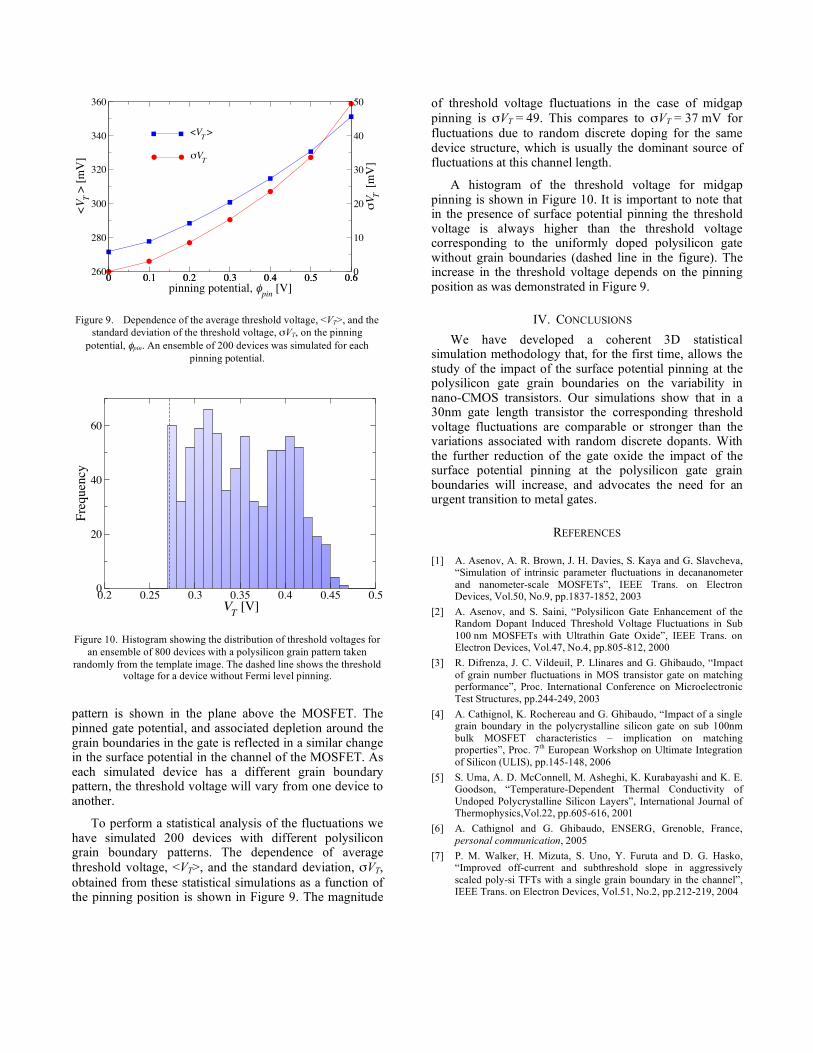
To perform a statistical analysis of the fluctuations we have simulated 200 devices with different polysilicon grain boundary patterns. The dependence of average
threshold voltage, <VT>, and the standard deviation, VT,
obtained from these statistical simulations as a function of the pinning position is shown in Figure 9. The magnitude
of threshold voltage fluctuations in the case of midgap
pinning is VT = 49. This compares to VT = 37 mV for
fluctuations due to random discrete doping for the same device structure, which is usually the dominant source of fluctuations at this channel length.
A histogram of the threshold voltage for midgap pinning is shown in Figure 10. It is important to note that in the presence of surface potential pinning the threshold voltage is always higher than the threshold voltage corresponding to the uniformly doped polysilicon gate without grain boundaries (dashed line in the figure). The increase in the threshold voltage depends on the pinning position as was demonstrated in Figure 9.
IV. CONCLUSIONS
We have developed a coherent 3D statistical simulation methodology that, for the first time, allows the study of the impact of the surface potential pinning at the polysilicon gate grain boundaries on the variability in nano-CMOS transistors. Our simulations show that in a 30nm gate length transistor the corresponding threshold voltage fluctuations are comparable or stronger than the variations associated with random discrete dopants. With the further reduction of the gate oxide the impact of the surface potential pinning at the polysilicon gate grain boundaries will increase, and advocates the need for an urgent transition to metal gates.
REFERENCES
[1] A. Asenov, A. R. Brown, J. H. Davies, S. Kaya and G. Slavcheva, “Simulation of intrinsic parameter fluctuations in decananometer
and nanometer-scale MOSFETs”, IEEE Trans. on Electron Devices, Vol.50, No.9, pp.1837-1852, 2003
[2] A. Asenov, and S. Saini, “Polysilicon Gate Enhancement of the Random Dopant Induced Threshold Voltage Fluctuations in Sub
100 nm MOSFETs with Ultrathin Gate Oxide”, IEEE Trans. on Electron Devices, Vol.47, No.4, pp.805-812, 2000
[3] R. Difrenza, J. C. Vildeuil, P. Llinares and G. Ghibaudo, “Impact
of grain number fluctuations in MOS transistor gate on matching performance”, Proc. International Conference on Microelectronic
Test Structures, pp.244-249, 2003
[4] A. Cathignol, K. Rochereau and G. Ghibaudo, “Impact of a single grain boundary in the polycrystalline silicon gate on sub 100nm
bulk MOSFET characteristics – implication on matching properties”, Proc. 7th European Workshop on Ultimate Integration
of Silicon (ULIS), pp.145-148, 2006
[5] S. Uma, A. D. McConnell, M. Asheghi, K. Kurabayashi and K. E. Goodson, “Temperature-Dependent Thermal Conductivity of
Undoped Polycrystalline Silicon Layers”, International Journal of Thermophysics,Vol.22, pp.605-616, 2001
[6] A. Cathignol and G. Ghibaudo, ENSERG, Grenoble, France,
personal communication, 2005
[7] P. M. Walker, H. Mizuta, S. Uno, Y. Furuta and D. G. Hasko, “Improved off-current and subthreshold slope in aggressively
scaled poly-si TFTs with a single grain boundary in the channel”, IEEE Trans. on Electron Devices, Vol.51, No.2, pp.212-219, 2004
0 0.1 0.2 0.3 0.4 0.5 0.6pinning potential, φ
pin [V]
0
10
20
30
40
50
σV T
[m
V]
σVT
0 0.1 0.2 0.3 0.4 0.5 0.6260
280
300
320
340
360
<V T
> [
mV
]
<VT
>
Figure 9. Dependence of the average threshold voltage, <VT>, and the
standard deviation of the threshold voltage, VT, on the pinning
potential, pin. An ensemble of 200 devices was simulated for each
pinning potential.
0.2 0.25 0.3 0.35 0.4 0.45 0.5VT [V]
0
20
40
60
Freq
uenc
y
Figure 10. Histogram showing the distribution of threshold voltages for
an ensemble of 800 devices with a polysilicon grain pattern taken
randomly from the template image. The dashed line shows the threshold voltage for a device without Fermi level pinning.