iic - integrated inductive components
TRANSCRIPT

technical note
PhilipsComponents
IICIntegratedInductive
Components

1
Contents
Introduction 3
Features and Applications 4
Design example 8
Materials 9
Type Number structure 14
Environmental aspects 14
Product range 14
General product data 15
Product specifications 16
Reliability and Quality Control 20
Soldering and recommended solder lands 21
Packing 22
Storage requirements 23
IICIntegrated Inductive Components

2
Fig.1 View inside an IIC10 model

3
IntroductionFor the majority of today’s designs it is desirable to havelow profile inductive components. This allows designersnot only to make low profile equipment, but also to placethe inductive device anywhere on the PCB withoutadaptations to the housing. This is especially true whenthe inductive component matches the height of othercomponents on the board, for instance IC’s which areusually about 3mm high.
One way to achieve this objective is to simply lowerexisting core designs like E- or RM cores. When thesecores get really flat it becomes difficult to accommodatethe windings, especially if these must be able to carry largecurrents.
Windings can be flattened to adapt them to the shape ofthe component, as in planar magnetics. In the fullyintegrated planar device the possibility to use the copperlayer on the PCB as a winding is exploited for the firsttime.
Another way to do this is demonstrated in the newIntegrated Inductive Component (IIC), presented in thisbrochure. This product consists of a rectangular ferritesleeve with an inserted copper lead frame. This sleeve ispressed in one piece although the slot is only 0.75 mmhigh, and it can also comprise a partial airgap. The leadframe is surrounded by a moulding of a high tech resinto keep the leads together and to insulate them from theferrite core. After insertion the leads are bent in a so-called gull wing shape to form contact pads, just like withmost standard SMD IC’s.In fact, the finished product really looks like an IC fromthe outside. It closely resembles the SOT outline and canbe handled by standard pick and place equipment as wellas soldered together with other IC’s on the board.
The leads in the moulding form one half of a windingwhich is completed by a track on the PCB. In this way,depending on the PCB layout, one or more inductorswith up to 10 turns can be constructed. The same productcan be applied to make 1 inductor with 10 turns or 2with 5 turns etc.
The IIC design can perform several magnetic functions,depending on the material and the presence of a partialairgap.
core halveswinding
coil former
PCB tracks
PCB
ferrite core halves planar winding
multilayer PCB
ferrite core
PCB
moulded-in leads
PCB tracks
Fig.2 Three basic principles to make a low profile inductivecomponent.
LL
L×10
100 L
25 L 25 L
Fig.3 PCB track examples.

4
Applications
IIC with partial airgap
This product type has a partial airgap to improve energystorage capability. Its performance has all characteristicsof a stepped choke. Possible magnetic functions are:
• power inductor• output choke• EMI-choke with bias
Power inductors are applied as output choke in switchedmode power supplies, inductor in high frequenciesDC/DC (buck/boost) converters or resonant inductors inresonant converters. Because of the limited number ofturns the product will only be of interest for fairly highfrequencies (≥ 200 kHz).
IDC
L
no airgap
partial airgap
airgap
Fig.4 Inductance curve of an IIC choke with a partial airgapcompared to the curves for products without and with a full airgap.
Features• Inductive SMD component that looks like a standard IC outline (SOT).
• Windings are completed by PCB tracks.• Automatic placement and soldering together with other IC’s on the board.
• Suitable for reflow soldering.• Wide range of magnetic functions can be realized with the same product, depending on track layout.
• Superior physical properties.• Available in standard EIA and EIAJ tape-and-reel.• Operating temperature -55°C to +150°C.
The curves of L as a function of DC bias exhibit theeffect of a partial airgap. For comparison, curves forproducts with a complete airgap and without are shownin Fig.4. For all these applications saturation flux densityshould be as high as possible with low power losses.Therefore 3C30 is the ideal material here. However forvery high frequencies (≥ 500 kHz) a better choice wouldbe 3F4.
EMI-chokes often suffer from saturation when usedwithout current compensation in line with elevated DC orAC bias currents. The design with a partial airgap avoidscomplete saturation to a large extend. The suppressioneffect remains at an acceptable level.
ferrite core leads
partial airgap saturation area
Cross-section of an IIC showing flux patterns and partial saturation.

5
For power inductors and transformers ferrite volume isone of the major parameters determining the throughputpower of the device. For this reason IIC products inpower materials have a standard height of 4 mm, but canalso be produced as a 3 mm high version.
Signal transformerFor signal transformers (pulse or wideband) it isimportant to have a high primary inductance. This levelcontrols low frequency performance. Our highpermeability material 3E6 helps to reach the requiredlevels in spite of the low number of turns.Required low leakage inductances can be obtained bymeans of a bifilar winding configuration (see Fig.7 onpage 6).Also in this application IIC10 is not suitable if a safetybarrier is required.
0.01 0.1 1 10
1
100
1
Switching Frequency (MHz)
10
ThroughputPower
(W)
Fig.5 Throughput power capability of IIC10-14/4-3F4 when applied asa power transformer. Practical values will also depend on circuittopology and switching techniques used. Therefore only a range is
indicated in the graph.
Fig.6 Inductance of IIC10-14/4-3E6 (10 turns) as a function offrequency.
IIC without partial airgapThis design is suitable for the following magneticfunctions:
• power transformer• signal transformer• common-mode choke
Power transformerIIC can perform as very flat power transformer inapplications like high frequency DC/DC converters (> 500 kHz) with low voltages and low power levels.The product is best applied at low input voltages andhigh switching frequencies because of the limited numberof turns. Although isolation voltage is specified as 500 V,the IIC10 should not be applied in AC/DC applicationsas safety isolation transformer. The short distance betweenthe leads makes it unsuitable for that function.There is a trend towards converters which bring down 5 Vto 3.3 V or even 2 V as supply for special IC’s.Especially in the case of a bifilar winding configurationleakage flux is low and coupling satisfactory for thetransformer function. At frequencies above 500 kHz themost suitable material is 3F4.
0
1000
1 10 102 103
500
L (µH)
f (kHz)
IIC10-14/4-3E6

1 10 102 103
10 3
f (MHz)
10 2
Z
(Ω)
IIC10-14/4-3S4 (N = 5)
5 turns
diffe
renti
al mod
e
1
10
5 tur
ns di
ffere
ntial
mode (
bifila
r)
5 tur
ns di
ffere
ntial
mod
e (bif
ilar,
satur
ated)
common mode differential mode
common modebifilar
differential modebifilar
5 turns common mode
Normal pattern IIC10
removewhenusedas5+5 turns
Bifilar pattern IIC10
6
Fig.7 Impedance curves of IIC10-14/4-3S4 connected as common-mode and differential-mode choke.
Fig.8 Unifilar recommended track pattern. Fig.9 Bifilar recommended track pattern.
Common-mode chokeMade in our top quality suppression material 3S4 or thehigh permeability material 3E6, the design is ideal ascommon- mode choke in signal or supply lines, especiallyif these carry large currents. The sturdy lead frame willtake almost any current surge without being damaged.
All sorts of signal lines in Telecom and EDP equipmentrequire suppression of HF noise generated by internaldigital processing. Requirements are a common-modeimpedance of at least 100 Ω over a very wide frequencyrange (10 - 1000 MHz) and, at the same time, adifferential impedance of less than 10 Ω at 1 MHz toallow the real signal to pass without too much damping.
Especially with a bifilar winding configuration thecoupling is excellent and differential damping will be low.
As expected 3S4 is the best material to obtain a highimpedance over a wide frequency range. With 3E6damping is already effective between 1 and 10 MHz. Incombination with capacitors IIC can be effective assupply line filter also for even lower frequencies.
For common-mode chokes build height is very importantsince they are often used on boards together with IC’s.Therefore the 3S4 product can also be made with a heightof only 3mm, equal to most standard IC’s.

7
V
RSW1
SW2VR1
100 kHz
ON
OFF
ON
OFF
IR
Ic
SW1
SW2
IR
Ic
increasing Ic100 mA (typ.)
10 A (typ.)
td td tdtb tb
Fig.11 Schematic of a saturable inductor and associated waveforms(with regulation)
Saturable inductorSaturable inductors can be used to regulate severalindependent outputs of an SMPS by blocking varyingamounts of energy from the secondary of the transformer.The circuits required are both simple and economic andcan be easily integrated.
Operating principlesWhen switch SW2 (Fig.11), representing a small transistor,is open, no reset current can flow through the winding ofthe saturable inductor. Because the saturable inductor hasa rectangular B-H loop (see Fig. 10), the flux remains atthe high level Br even when the driving field H has fallento zero. When switch SW1 is closed the voltage across theinductor causes a current rise in the winding. There is ashort delay (td) because the flux rises from Br to Bs. Afterthat the current sharply rises to its maximum value,limited only by the load impedance.
When in the next cycle witch SW2, is closed, a resetcurrent can flow and is regulated by the transistor.Resetting to -Hc, for instance, causes some extra delay (tb)because of the larger flux swing. Full reset causes a fluxswing of almost 2.Bs, resulting in a maximum delay (td +tb) and the blocking of a part of the energy flowing fromthe transformer to the load.
In this way a reset current in the order of 100 mA canregulate load currents in the order of 10 A or more,depending on the layout of the saturable inductor. Forthis reason the described circuit is called a magneticregulator or even magnetic amplifier. In the case off IICthe combined resistance in leads and tracks limits thethroughput current to approximately 4 A when all 10turns are used. In many cases less turns will be needed.Then some tracks can be connected in parallel, therebyincreasing the maximum current level.
The performance of the material 3R1 is comparable tothat of amorphous metal making it an excellent materialfor application in magnetic regulators. When 3R1 coresare driven exactly at their natural mechanical resonantfrequencies a magneto-elastic resonance will occur. Withlarge flux excursions and no mechanical damping,amplitudes can become so high that the maximum tensilestress of the ferrite is exceeded. Cracks or even breakage ofthe core could be the result. It is advised not to use thecores at their mechanical resonant frequencies or evensubharmonics (e.g. half this resonant frequency).The resonant frequency of IIC10-14/4 is approximately 180 kHz.
+B
+B
-B
-B
H for full reset
H for partial reset
Hc
Hc
-H -Hc
-Hc
Bs
Bs
Br
-Bs
-Bs
-Br
BH loop excursion during full blocking
BH loop excursion during partial blocking
+B
-B
Hc-H -Hc
Bs
-Bs
-Br
BH loop excursion during no blocking
Fig.10 Schematic of flux excursions in a saturable inductor.

8Philips Magnetic Products
Design example
VinVout
PH
ILIP
SIIC
10-14/4-3E6
PH
ILIP
SIIC
10-14/4-3F4
PHILIPSIIC10P-14/4-3F4
input
filter transformer
output
filter
Fig.12 Basic diagram of a design example to demonstrate the versatility of the IIC concept.
For the completely worked out design of the DC/DC converter shown above, please refer to the Application Note 10 Watt DC/DC Converter using IIC Magnetics.(9398 239 03011)

9
Material characteristics
MBW236
1 10 102
10 4
f (MHz)
µ’ ,s µ’’s
10 3
10 2
1010 1
3C30
µ’’s
µ’ s
Complexpermeability as a
function of frequency
5000
50 50 2500
MBW235
150
1000
2000
3000
4000
µ i
T ( C)o
3C30
25 50 250
500
0
MBW237
150
100
200
300
400
250H (A/m)
B(mT)
3C3025 oC100 oC
Initialpermeability as a
function oftemperature
3C30 SPECIFICATIONS
SYMBOL CONDITIONS VALUE UNIT
µi 25 °C; ≤10 kHz;0.1 mT
1800 ±20%
µa 100 °C; 25 kHz;200 mT
5000 ±25%
B 100 °C; 10 kHz;250 A/ m
≥370 mT
PV 100 °C; 25 kHz;200 mT
≤80 kW/m3
100 °C; 100 kHz;100 mT
≤80
100 °C; 100 kHz;200 mT
≈450
ρ DC; 25 °C ≈2 ΩmTC ≥240 °Cdensity ≈4800 kg/m3
0 40 80
800
600
200
0
400
MBW241
120T ( C)
Pv(kW/m )3
3C30
o
f(kHz)
B(mT)
200 100
100 100
25 200
100 200
MBW240
102 103
10 3
10
H (A/m)
10 4
µ∆
3C30
101
10 2
MBW239
102 10310
B (mT)1 10
10 4
Pv(kW/m )3
3C30
10 2
10 3
25 k
Hz
200
kHz
100
kHz
T = 100 oC
50 k
Hz
0 100 200 400
8000
6000
2000
0
4000
MBW238
300
µa
B (mT)
3C3025 oC
100 oC
Typical B-H loops
Amplitudepermeability as afunction of peak
flux density.
Incrementalpermeability as a
function of magneticfield strength.
Specific power loss asa function of peakflux density withfrequency as a
parameter.
Specific power loss forseveral frequency/flux
density combinations asa function oftemperature.

10Philips Magnetic Products
Material characteristics3F4 SPECIFICATIONS
SYMBOL CONDITIONS VALUE UNIT
µi 25 °C; ≤10 kHz;0.1 mT
900 ±20%
µa 100 °C; 25 kHz;200 mT
≈1700
B 25 °C; 10 kHz;250 A/m
≥350 mT
100 °C; 10 kHz;250 A/m
≥300 mT
PV 100 °C; 1 MHz;30 mT
≤200 kW/m3
100 °C; 3 MHz;10 mT
≤320 kW/m3
ρ DC; 25 °C ≈10 Ωm
TC ≥220 °Cdensity ≈4700 kg/m3
2000
50 50 2500
MBW034
150
500
1000
1500
µ i
T ( C)o
3F4
0 100 200 400
2000
1500
500
0
1000
MBW046
300
µa
B (mT)
3F425 oC
100 oC
50 100 1000
500
0
MBW017
500
100
200
300
400
500H (A/m)
B(mT)
3F425oC
100oC
MBW025
1 10 102
10 4
f (MHz)
µ' ,s µ''s
10 3
10 2
1010 1
3F4
µ''s
µ' s
Complexpermeability as a
function of frequency
Typical B-H loops
Initialpermeability as a
function oftemperature
0 40 80
400
300
100
0
200
MBW056
120T ( C)
Pv(kW/m )3
3F4
o
f(kHz)
B(mT)
1000 30
500 50
3000 10
1000 25
MBW047
102 10310
B (mT)1 10
10 4
Pv(kW/m )3
3F4
10 2
10 3
1 M
Hz
400
kHz
25 k
Hz
200
kHz
100
kHz
2 M
Hz
3 M
Hz
T = 100 oC
MBW035
102 103
10 3
10
H (A/m)
10 4
µ∆
3F4
101
10 2
Amplitudepermeability as afunction of peak
flux density.
Incrementalpermeability as a
function of magneticfield strength.
Specific power loss asa function of peakflux density withfrequency as a
parameter.
Specific power loss forseveral frequency/fluxdensity combinations
as a function oftemperature.

11
Material characteristics3E6 SPECIFICATIONS
Note
1. Measured on sintered, non-ground ring cores ofdimensions Ø14 × Ø9 × 5 which are not subjected toexternal stresses.
SYMBOL CONDITIONS VALUE (1) UNIT
µi 25 °C; ≤10 kHz;0.1 mT
12000 ±20%
B 25 °C; 10 kHz;250 A/ m
≈380 mT
100 °C; 10 kHz;250 A/ m
≈210
tanδ/µi 25 °C; 10 kHz;0.1 mT
≤10 × 10−6
25 °C; 30 kHz;0.1 mT
≤30 × 10−6
ηB 25 °C; 10 kHz;1.5 to 3 mT
≤1 × 10⁻³ T−1
ρ DC; 25 °C ≈0.1 ΩmTC ≥130 °Cdensity ≈4900 kg/m3
MBW267
102 103
10 4
H (A/m)
10 5
µ∆
3E6
101
10 3
102
25 50 250
500
0
MBW266
150
100
200
300
400
250H (A/m)
B(mT)
3E625 oC100 oC
MBW264
10 1 10
10 5
f (MHz)
µ’ ,s µ’’s
10 4
10 3
1010 2
3E6
µ’’s
2
1
µ’ s
40000
50 50 2500
MBW265
150
10000
20000
30000
µ i
T ( C)o
3E6
Complexpermeability as a
function of frequency
Initialpermeability as a
function oftemperature
Typical B-H loops
Incrementalpermeability as a
function of magneticfield strength.

12Philips Magnetic Products
Material characteristics
5000
50 50 2500
MBW191
150
1000
2000
3000
4000
3S4µi
T (oC)
MBW195
1 10 102
10 4
f (MHz)
µ' ,s µ''s
10 3
10 2
1010 1
3S4
µ''s
µ' s
50 100 1000
500
0
MBW199
500
100
200
300
400
500H (A/m)
B(mT)
3S425oC
100oC150
0
100
1
MBW221
10 102 103
50
Z(Ω)
f (MHz)
3S4
3S4 SPECIFICATIONS
Note
1. Measured on a bead ∅5× ∅2 × 10 mm
Remark: This wideband EMI-suppression material isoptimized for applications without bias currents atmoderate temperatures (e.g. common-mode chokes).
SYMBOL CONDITIONS VALUE UNIT
µi 25 °C; ≤10 kHz;0.1 mT
≈1700
B 25 °C; 10 kHz;250 A/ m
≈300 mT
100 °C; 10 kHz;250 A/ m
≈140
Z(1) 25 °C; 3 MHz; ≥25 Ω25 °C; 30 MHz; ≥6025 °C; 100 MHz; ≥8025 °C; 300 MHz; ≥90
ρ DC, 25 °C ≈103 ΩmTC ≥110 °Cdensity ≈4800 kg/m3
Complexpermeability as a
function of frequency
Initialpermeability as a
function oftemperature
Typical B-H loopsImpedance as a
function of frequency.

13
MBW061
1 10 102
10 4
f (MHz)
µ’ ,s µ’’s
10 3
10 2
1010 1
3R1
µ’’s
µ’ s
Complexpermeability as a
function of frequency
5000
50 50 2500
MBW062
150
1000
2000
3000
4000
µ i
T ( C)o
3R1
50 100 1000
500
0
MBW018
500
100
200
300
400
500H (A/m)
B(mT)
3R125oC
100oC
Initialpermeability as a
function oftemperature
3R1 SPECIFICATIONS
SYMBOL CONDITIONS VALUE UNIT
µi 25 °C; ≤10 kHz;0.1 mT
800 ±20%
B 25 °C; 10 kHz;250 A/ m
≥360 mT
100 °C; 10 kHz;250 A/ m
≥285
Br from 1 kA/m; 25 °C ≥310 mTfrom 1 kA/m; 100 °C ≥220
Hc from 1 kA/m; 25 °C ≤52 A/mfrom 1 kA/m; 100 °C ≤23
ρ DC; 25 °C ≈103 ΩmTC ≥230 °Cdensity ≈4700 kg/m3
0 40 80
800
600
200
0
400
MBW002
120T ( C)
Pv(kW/m )3
3R1
o
f(kHz)
B(mT)
100 100
30 200
10 200
MBW001
102 10310
B (mT)1 10
10 4
Pv(kW/m )3
3R1
10 2
10 3
1 MHz
400 kHz
10 kHz
25 kHz
100 kHz
Typical B-H loops
Specific power loss asa function of peakflux density withfrequency as a
parameter.
Specific power loss forseveral frequency/flux
density combinations asa function oftemperature.
Warning:When 3R1 cores are driven exactly at their naturalmechanical resonant frequencies a magneto-elasticresonance will occur. With large flux excursions and nomechanical damping, amplitudes can become so high thatthe maximum tensile stress of the ferrite is exceeded.Cracks or even breakage of the core could be the result. Itis advised not to drive the cores at their resonantfrequencies or even subharmonics (e.g. half this resonant frequency).
Material characteristics

14
Type Number structureType Numbers for these products consists of 3 parts:
1. Product type2. Size (A/B)3. Ferrite material
IIC10P - 14/4 - 3C30_______ _______ _____
1 2 3
1.Product TypeIIC: Integrated Inductive Component10: Number of leadsP: Partial gap
2.Size A/BA: widthB: height
Product RangeIIC10P-14/4-3C30IIC10P-14/4-3F4IIC10-14/4-3F4IIC10-14/4-3E6IIC10-14/4-3S4IIC10-14/4-3R1
Environmental aspectsFerriteOur range of soft ferrites has the general compositionMeFe2O4 where Me represents one or several of thedivalent transition metals such as manganese (Mn), zinc(Zn), nickel (Ni), or magnesium (Mg).To be more specific, all materials starting with digit 3 aremanganese zinc ferrites based on the MnZn composition.Their general chemical formula is:Mnδ Zn(1-δ)Fe2O4Materials starting with digit 4 are nickel zinc ferritesbased on the NiZn composition. Their general chemicalformula is:Niδ Zn(1-δ)Fe2O4
Leadframe
Leadframe material:copper, plated with tin-lead alloy (SnPb 85/15)
Moulding material:liquid crystal polymer (LCP), flame retardant inaccordance with UL 94V-0.
General warning rules• With strong acids, the metals iron, manganese,nickel and zinc may be partially extracted.
• In the event of fire, dust particles with metaloxides will be formed.
• Disposal as industrial waste, depending on local rules and circumstances.

15Philips Magnetic Products
Effective core parameters
SYMBOL PARAMETER VALUE UNIT
Σ(l/A) core factor (C1) 2.47 mm-1
Ve effective volume 338 mm3
le effective length 28.9 mm
Ae effective area 11.7 mm2
m mass ~ 1.85 g
0.1
14.4 ± 0.2
4 ± 0.08
2.7 ± 0.2
7.2 ± 0.15
10.45 max
4.38 max
0.3 max1.0 0.6 max
0.75
0.1
14.4 ± 0.2
4 ± 0.08
2.7 ± 0.2
1.0 0.6 max
0.75
Fig.13 IIC10P-14/4 and IIC10-14/4 outline
General product data
General data
Rdc:~ 65 mΩ (25°C) and ~85 mΩ (100°C) for 10 turnsincluding 20 solder joints (assuming 70 µm Cu PCB tracks)
Leadframe material:copper, plated with tin-lead alloy (SnPb 85/15)
Solderability:- compatible with reflow soldering- IEC 68-2-58, part2, test Ta, method 1
Moulding material:liquid crystal polymer (LCP), flame retardant inaccordance with UL 94V-0.
Isolation voltage:> 500 Vdc between leads and between leads and ferritecore.
Isolation resistance:>100 MΩ between leads .
Inter winding capacitance:2 windings of 5 turns- unifilar ~ 5 pF- bifilar ~ 10 pF(depending on track layout)
Leakage inductance:2 windings of 5 turns- unifilar ~ 1.8 µH- bifilar ~ 0.2 µH
Maximum continuous current (DC):4 A (depending on thickness of copper tracks on PCB)
Maximum peak current:10 A
16
Product specification IIC10P-14/4-3C30
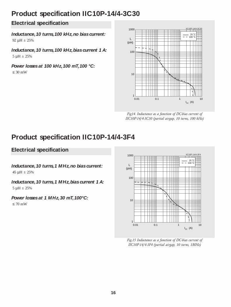
Electrical specification
Inductance,10 turns,1 MHz,no bias current:45 µH ± 25%
Inductance,10 turns,1 MHz,bias current 1 A:5 µH ± 25%
Power losses at 1 MHz,30 mT,100°C:≤ 70 mW
0.01 0.1 1 101
1000
10
IDC (A)
100
L(µH)
25 oC100
oC
IIC10P-14/4-3C30
Fig14. Inductance as a function of DC-bias current of IIC10P-14/4-3C30 (partial airgap, 10 turns, 100 kHz)
Electrical specification
Inductance,10 turns,100 kHz,no bias current:92 µH ± 25%
Inductance,10 turns,100 kHz,bias current 1 A:5 µH ± 25%
Power losses at 100 kHz,100 mT,100 °C:≤ 30 mW
Product specification IIC10P-14/4-3F4
0.01 0.1 1 101
1000
10
IDC (A)
100
L(µH)
25 oC100
oC
IIC10P-14/4-3F4
Fig.15 Inductance as a function of DC-bias current of IIC10P-14/4-3F4 (partial airgap, 10 turns, 1MHz)

17Philips Magnetic Products
Product specification IIC10-14/4-3F4
0.01 0.1 1 10 100f (MHz)
1
10
100
|Z|(Ω)
IIC10-14/4-3E6
Fig.18 Impedance per lead of IIC10-14/4-3E6 (1 turn) as a functionof frequency.
0
10
1 10 102 103
5
L (µH)
f (kHz)
IIC10-14/4-3E6
Fig.17 Inductance of IIC10-14/4-3E6 (1 turn) as a function offrequency.
Electrical specification
Inductance per line,1 MHz,no bias current:0.45 µH ± 25%
Power losses at 1 MHz,30 mT,100°C:≤ 70 mW
Product specification IIC10-14/4-3E6
0
0.2
0.4
0.6
0.8
1
0.01 0.1 1 10 100f (MHz)
L(µH)
IIC10-14/4-3F4
Fig.16 Inductance of IIC10-14/4-3F4 (1 turn) as a function offrequency.
Electrical specification
Inductance per line,10 kHz,no bias current:6 µH ± 30%

18
Product specification IIC10-14/4-3S4
1
10
100
1000
1 10 100 1000f (MHz)
|Z|(Ω)
1
2
3
4
5
IIC10-14/4-3S4
Fig.19 Impedance curves of IIC10-14/4-3S4 with the number of turnsas a parameter.
Electrical specification
Typical impedance per line at 100 MHz:Ztyp ~ 35 Ω
Minimum guaranteed value is typical -20%
1
10
100
1000
1 10 100 1000f (MHz)
|Z|(Ω) 0 A
1 A
2 A
3 A
0.2 A
0.5 A
IIC10-14/4-3S4
Fig.22 Impedance curves of IIC10-14/4-3S4 for 5 turns with biascurrent as a parameter.
1 10 100 1000f (MHz)
1
10
100
|Z|(Ω)
Outer line
Inner line
IIC10-14/4-3S4
Fig.20 Impedance curves of IIC10-14/4-3S4 for a single inner andouter lead.
0.1
1
10
100
1 10 100 1000f (MHz)
|Z|(Ω)
0A
3A
5A
7A
1A
IIC10-14/4-3S4
Fig.21 Impedance curves of IIC10-14/4-3S4 for a single outer leadwith bias current as a parameter.
19
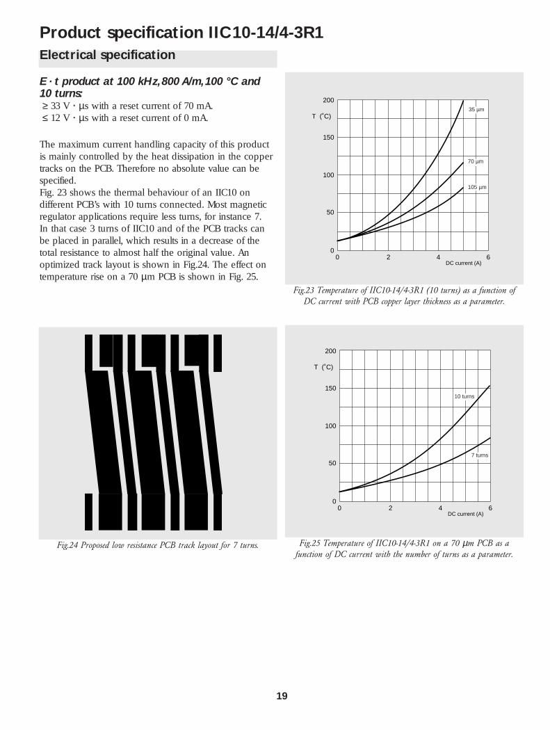
Product specification IIC10-14/4-3R1Electrical specification
E . t product at 100 kHz,800 A/m,100 °C and10 turns:≥ 33 V . µs with a reset current of 70 mA.≤ 12 V . µs with a reset current of 0 mA.
The maximum current handling capacity of this productis mainly controlled by the heat dissipation in the coppertracks on the PCB. Therefore no absolute value can bespecified.Fig. 23 shows the thermal behaviour of an IIC10 ondifferent PCB’s with 10 turns connected. Most magneticregulator applications require less turns, for instance 7.In that case 3 turns of IIC10 and of the PCB tracks canbe placed in parallel, which results in a decrease of thetotal resistance to almost half the original value. Anoptimized track layout is shown in Fig.24. The effect ontemperature rise on a 70 µm PCB is shown in Fig. 25.
200
0 2 60
4
50
100
150
T (˚C)
DC current (A)
35 µm
70 µm
105 µm
Fig.23 Temperature of IIC10-14/4-3R1 (10 turns) as a function ofDC current with PCB copper layer thickness as a parameter.
200
0 2 60
4
50
100
150
T (˚C)
DC current (A)
7 turns
10 turns
Fig.25 Temperature of IIC10-14/4-3R1 on a 70 µm PCB as afunction of DC current with the number of turns as a parameter.
Fig.24 Proposed low resistance PCB track layout for 7 turns.

20Philips Magnetic Products
Reliability and Quality Controls
TEST IEC NORM /REFERENCE
CONDITIONS
A. Climaticnon operational & non packed(1) Cold IEC 68-2-1 Ab 96 hours at -25˚C(2) Dry Heat IEC 68-2-2 Bb 96 hours at +110˚C(3) Damp Heat (cyclic) IEC 68-2-30 Db 21 days between +25 and +40˚C at 95% RH(4) Damp Heat (steady state) IEC 68-2-30 Ca 21 days at +40˚C and 93%RH(5) Thermal Cycling IEC 68-2-14 Nb 5 cycles between -55˚C and +150˚CB. Mechanicalnon operational & non packed(6) Vibration (sinusoidal) IEC 68-2-6 Fc frequency range 10-55-10 Hz
amplitude 0.35 mm - 3 axis30 minutes per axis
(7) Bump IEC 68-2-29 Eb peak acceleration: 245 m/s2 (25 g)number of bumps: 1000 per directionnumber of directions: 6
(8) Shock IEC 68-2-27 Ea duration of pulse: 11 mspulse shape: half-sinenumber of directions: 6number of shocks: 3 per directionpeak acceleration: 490 m/s2 (50 g)
(9) Robustness of Terminations IEC 68-2-20 Ub method 1(10) Resistance to Soldering Heat IEC 68-2-20 Tb method 1A
5 ± 1 sec at 260 ± 5˚C(11) Solderability IEC 68-2-20 Ta
(no extra aging e.g15 hours at 155˚C)
first part method 12 ± 0.5 sec at 235 ± 5˚C
(12) Flammability UL 94 V0 (0.81 mm)
Requirements after Tests
Test
(1)(2)(3)(4)(5)(6)(7)(8)(9)(10)(11)
Electrical (change L)
< 5%< 5%< 5%< 5%< 5%< 5%< 5%< 5%
Mechanical
no changesno changesno changesno changesno changesno changesno changesno changesno changesno changes> 95% wetted surface
PHILIPS COMPONENTS IIC’s are submitted toextensive tests to ensure high quality, high reliability andcomplete customer satisfaction. A survey is given below.

21
The advantages of good solderability of both componentsand substrate can be summarized as follows:
1. Lower soldering temperatures and shorter dwell timesprevent damage to devices or dissolution of metallization.The thickness of inter-metallic zones is minimized, thusincreasing mechanical integrity and providing a stableelectrical connection.
2. It permits the use of a less active flux. Therefore theflux residue activity is low and cleaning the substrate maybe unnecessary.
3. Better cost effectiveness by shorter production timesowing to less re-working and repairs.
PHILIPS COMPONENTS Integrated InductiveComponents are suitable for reflow soldering.Recommended temperature profiles for both methods aregiven below.
For repairing soldered joints, recommended settings350°C, within 5 seconds.
1.4
1.1
1.0
0.9 0.6 0.5
10.958.15
clearance solder lands solder paste
Fig.26 Recommended temperature profile for reflow soldering.
Soldering
Recommended solder lands
Fig.27 Recommended solder lands.
Preheat100 sec max.
Soldering10 sec max.
Naturalcooling
60 sec min.
215 - 280oC
180oC
160oC max1 min. max.
α = 10 K/s max.

22Philips Magnetic Products
PHILIPS COMPONENTS IIC’s are delivered taped andreeled, ready for use in automatic pick-and-placemachines, according to IEC 286-B and EIA 481-2.
ReelReels size is 330mm (13 inch), with approximately 1000products.
SIZE PACKING QUANTITYIIC10-14/4 1000IIC10P-14/4 1000
12.7
5 +
0.1
5
20.5
100
± 5
330
± 2
< 28.4
Packing quantities
Fig.28 Dimensions of reel
Packing

23
SIZE A0 B0 W T D0 D1 P0 P1 K0
IIC10-14/4 10.6±0.1 14.75±0.1 24±0.3 0.3 1.5±0.1 1.5±0.25 4.0±0.1 12±0.1 4.75 ±0.1
Storage requirementsStorage requirements advised here should be observed inorder to ensure the soldering of the exposed electrode:
• Maximum ambient temperature shall not exceed 40°C.Storage temperature higher than 40°C could result indeformation of packaging materials.• Maximum relative humidity recommended for storageis 70%. High humidity with high temperature canaccelerate the oxidation of the tin-lead plating on thetermination and reduce the solderability of thecomponents.• Products shall not be stored in environments with thepresence of harmful gases containing sulfur or chlorine.
W
P 0D 0
B0
A0 D1
P1
direction of unreeling
KT 0
cover tape
cover film
blister tape
direction ofunreeling
Fig29. Dimensions of blister tape