ihs 3: test of digital systems · ihs 3: test of digital systems ... • digital systems testing...
TRANSCRIPT
Integrierte Hard- und Softwaresysteme
IHS 3: Test of Digital Systems
R.Ubar, A. Jutman, H-D. Wuttke

Technical University Tallinn, ESTONIACopyright 2000-2003 by Raimund Ubar
2
Organisatorisches
Nächste Termine: Blockveranstaltung Dr. Jutman23.1. 24.1. 2014

Technical University Tallinn, ESTONIACopyright 2000-2003 by Raimund Ubar
3
Experiments
• Use the example A+B/2 (avarage value)• Find for each test method best parameters
– Functional test– Deterministic test– Functional BIST– Logical BIST– Circular BIST
• Note them and compare results
Technical University Tallinn, ESTONIACopyright 2000-2003 by Raimund Ubar
4
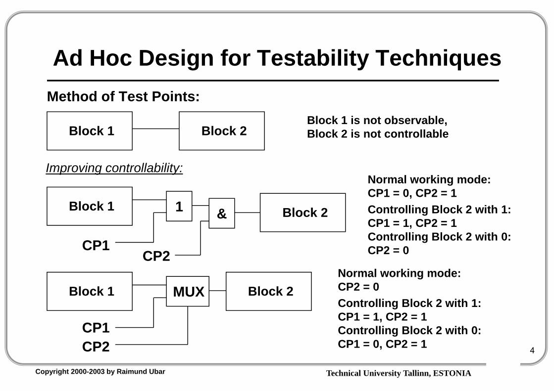
Ad Hoc Design for Testability TechniquesMethod of Test Points:
Block 1 Block 2Block 1 is not observable,Block 2 is not controllable
Block 1 Block 21
CP1
Improving controllability:
Block 1 Block 2
Normal working mode:CP1 = 0, CP2 = 1 Controlling Block 2 with 1:CP1 = 1, CP2 = 1Controlling Block 2 with 0:CP2 = 0
MUX
CP1
&
CP2
CP2
Normal working mode:CP2 = 0 Controlling Block 2 with 1:CP1 = 1, CP2 = 1Controlling Block 2 with 0:CP1 = 0, CP2 = 1

Technical University Tallinn, ESTONIACopyright 2000-2003 by Raimund Ubar
5
Website for this imageConsider i- Corporation for your
quality custom test fixtures. Bed of Nails ...icorporation.biz
http://www.youtube.com/watch?v=EHsZQ1WiojE
Technical University Tallinn, ESTONIACopyright 2000-2003 by Raimund Ubar
6
Boundary Scan Standard
http://www.youtube.com/watch?v=0YOBZ122vI0
Technical University Tallinn, ESTONIACopyright 2000-2003 by Raimund Ubar
7
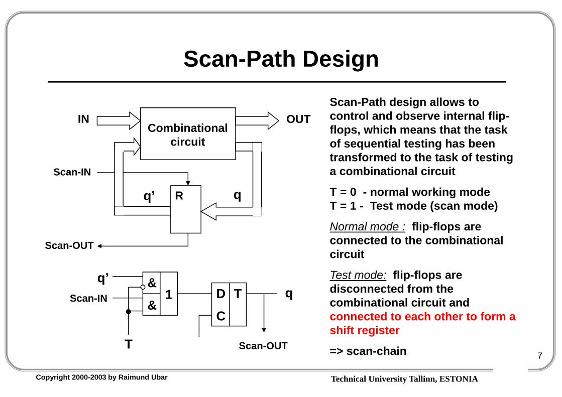
Scan-Path Design
Combinational circuit
IN OUT
R
Scan-IN
Scan-OUT
1&&
q
q’Scan-IN
T
TDC
Scan-OUT
q
q’
Scan-Path design allows to control and observe internal flip-flops, which means that the task of sequential testing has been transformed to the task of testing a combinational circuit
T = 0 - normal working mode T = 1 - Test mode (scan mode)
Normal mode : flip-flops are connected to the combinational circuit
Test mode: flip-flops are disconnected from the combinational circuit and connected to each other to form a shift register
=> scan-chain

Technical University Tallinn, ESTONIACopyright 2000-2003 by Raimund Ubar
8
Scan-Path Design and Testability
OUTMUX
DMUXIN
SCANOUT
SCANIN
Two possibilities for improving controllability/ observability

Technical University Tallinn, ESTONIACopyright 2000-2003 by Raimund Ubar
9
Parallel Scan-Path
Combinational circuit
IN OUT
R1
Scan-IN 1
Scan-OUT 1
R2
Scan-IN 2
Scan-OUT 2
In parallel scan path flip-flops can be organized in more than one scan chain

Technical University Tallinn, ESTONIACopyright 2000-2003 by Raimund Ubar
10
Boundary Scan Standard
Technical University Tallinn, ESTONIACopyright 2000-2003 by Raimund Ubar
11
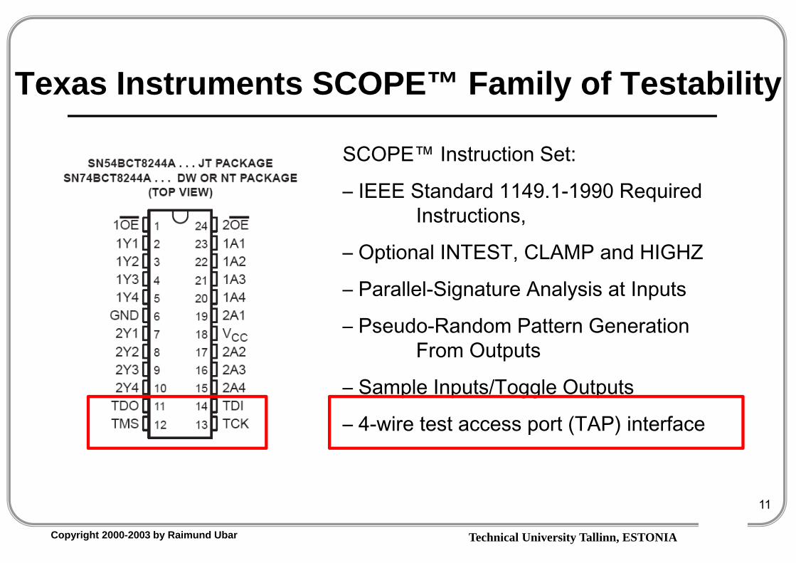
Texas Instruments SCOPE™ Family of Testability
SCOPE™ Instruction Set:
– IEEE Standard 1149.1-1990 Required Instructions,
– Optional INTEST, CLAMP and HIGHZ
– Parallel-Signature Analysis at Inputs
– Pseudo-Random Pattern Generation From Outputs
– Sample Inputs/Toggle Outputs
– 4-wire test access port (TAP) interface
Technical University Tallinn, ESTONIACopyright 2000-2003 by Raimund Ubar
12
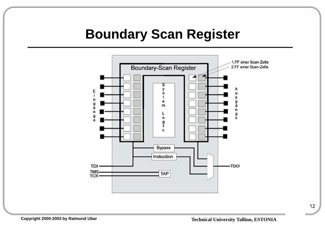
Boundary Scan Register
Technical University Tallinn, ESTONIACopyright 2000-2003 by Raimund Ubar
13
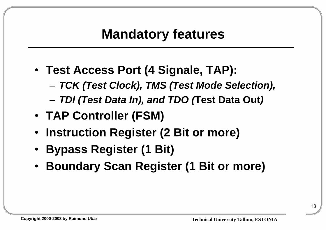
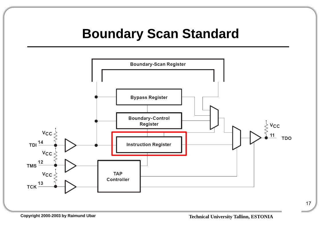
Mandatory features
• Test Access Port (4 Signale, TAP):– TCK (Test Clock), TMS (Test Mode Selection), – TDI (Test Data In), and TDO (Test Data Out)
• TAP Controller (FSM)• Instruction Register (2 Bit or more)• Bypass Register (1 Bit)• Boundary Scan Register (1 Bit or more)
Technical University Tallinn, ESTONIACopyright 2000-2003 by Raimund Ubar
14
Boundary Scan Standard

Technical University Tallinn, ESTONIACopyright 2000-2003 by Raimund Ubar
15
Boundary Scan Standard

Technical University Tallinn, ESTONIACopyright 2000-2003 by Raimund Ubar
16
Boundary Scan Standard 1149.1-1990
Serial-test information is conveyed by means of a 4-wire test bus, or test access port (TAP), that conforms to IEEE Standard 1149.1-1990
Test instructions, test data, and test control signals all are passed along this serial-test bus.
The TAP controller monitors two signals from the test bus, TCK (clock) and TMS (mode select).
Technical University Tallinn, ESTONIACopyright 2000-2003 by Raimund Ubar
17
Boundary Scan Standard

Technical University Tallinn, ESTONIACopyright 2000-2003 by Raimund Ubar
18
Instruction-Register Opcodes

Technical University Tallinn, ESTONIACopyright 2000-2003 by Raimund Ubar
19
Instruction-Register Opcodes

Technical University Tallinn, ESTONIACopyright 2000-2003 by Raimund Ubar
20
Instruction-Register Opcodes
Technical University Tallinn, ESTONIACopyright 2000-2003 by Raimund Ubar
21
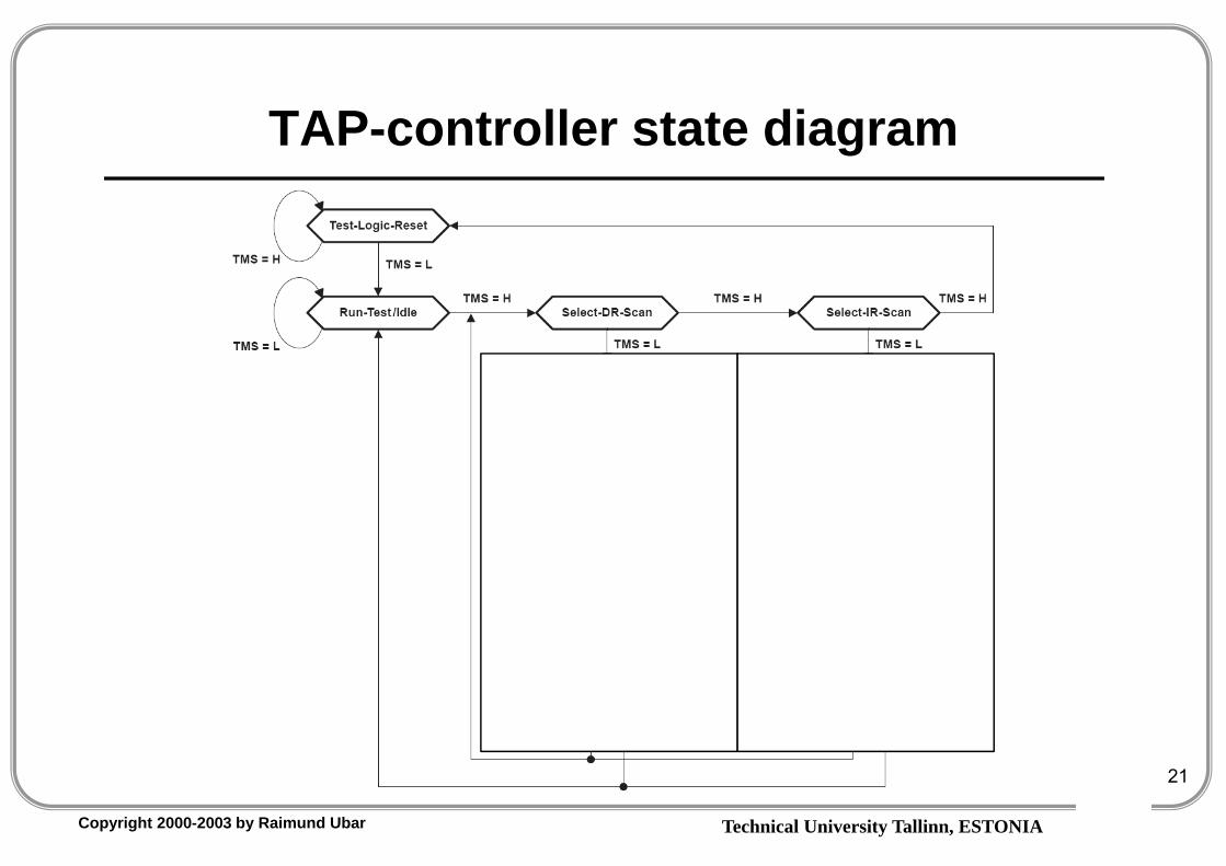
TAP-controller state diagram
Technical University Tallinn, ESTONIACopyright 2000-2003 by Raimund Ubar
22
TAP-controller state diagram

Technical University Tallinn, ESTONIACopyright 2000-2003 by Raimund Ubar
23
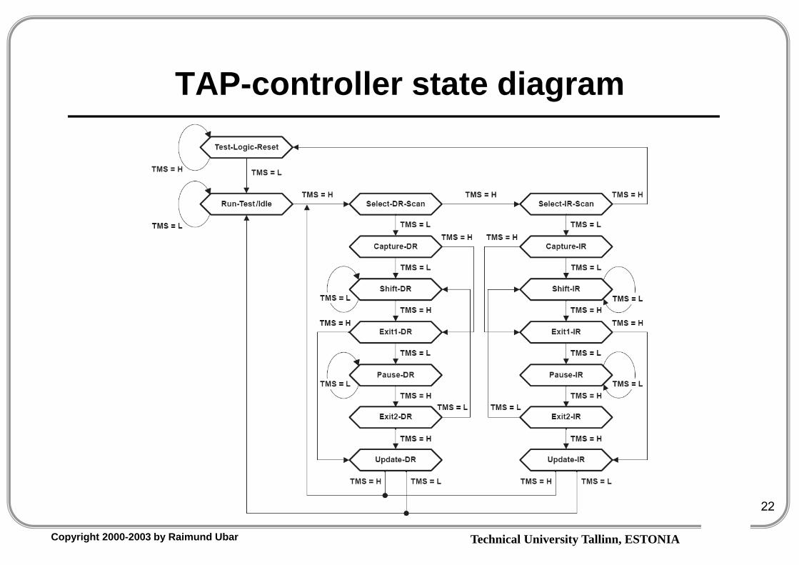
Boundary Scan States
•To reach state “Pause-DR”
select state sequence:
•TMS=0 > Run-Test/Idle
•TMS=1 > Select-DR-Scan,
•TMS=0 > Capture-DR,
•TMS=0 > Shift-DR, and
•TMS=1> Exit1-DR
•TMS=0 > Pause-DR
Technical University Tallinn, ESTONIACopyright 2000-2003 by Raimund Ubar
24
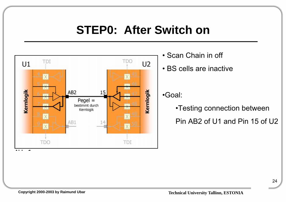
STEP0: After Switch on
• Scan Chain in off
• BS cells are inactive
•Goal:
•Testing connection between
Pin AB2 of U1 and Pin 15 of U2

Technical University Tallinn, ESTONIACopyright 2000-2003 by Raimund Ubar
25
STEP1: SAMPLE/PRELOAD
• Testing connection between Pin AB2 of U1 and Pin 15 of U2
• Preload
• FF 5 U1: control
• FF 6 U1: output
• FF 7 U1: input
• FF 5 =“1” => Driver at FF 6 active
• Pin AB2 = 1
4
5
6
7
8
9
4546
47
48
49
50

Technical University Tallinn, ESTONIACopyright 2000-2003 by Raimund Ubar
26
STEP2: SAMPLE/PRELOAD
• Driving AB2 of U1 with “1”
• Scan chain is activated
• Scan cells are inactive (x)4
5
6
7
8
9
4546
47
48
49
50

Technical University Tallinn, ESTONIACopyright 2000-2003 by Raimund Ubar
27
STEP3: EXTEST
• Test vector loaded
• Scan cells active
• FF 6 U1 drives “1”
• Pin 15 U2: tri state (inactive)
• Measuring
• U1: at FF 7
• U2 at FF 48
Technical University Tallinn, ESTONIACopyright 2000-2003 by Raimund Ubar
28
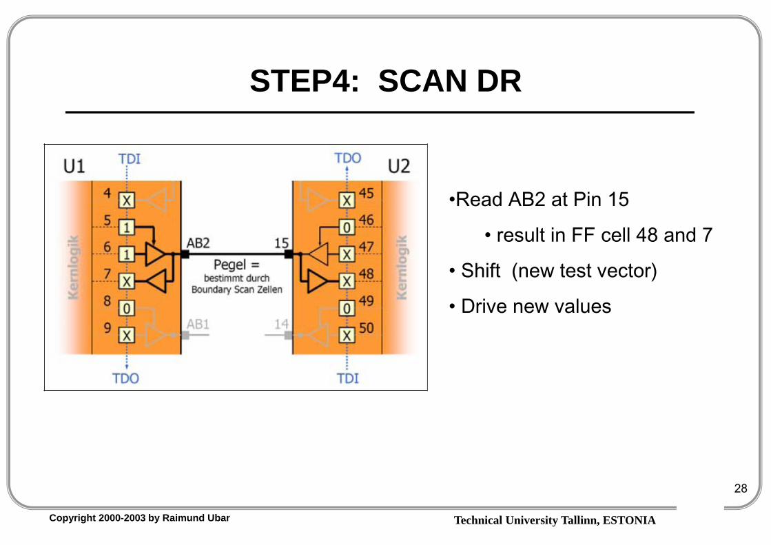
STEP4: SCAN DR
•Read AB2 at Pin 15
• result in FF cell 48 and 7
• Shift (new test vector)
• Drive new values
Technical University Tallinn, ESTONIACopyright 2000-2003 by Raimund Ubar
29
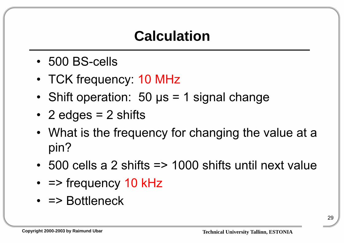
Calculation
• 500 BS-cells• TCK frequency: 10 MHz• Shift operation: 50 μs = 1 signal change• 2 edges = 2 shifts• What is the frequency for changing the value at a
pin?• 500 cells a 2 shifts => 1000 shifts until next value• => frequency 10 kHz• => Bottleneck

Technical University Tallinn, ESTONIACopyright 2000-2003 by Raimund Ubar
30
Boundary Scan Applet

Technical University Tallinn, ESTONIACopyright 2000-2003 by Raimund Ubar
31
Boundary Scan Diagnosis

Technical University Tallinn, ESTONIACopyright 2000-2003 by Raimund Ubar
32
References
• Books:• Boundary Scan Handbook, 3rd Edition, Ken P. Parker,
Kluwer Academic Publishers, ISBN 1-4020-7496-4• Analog and Mixed-Signal Boundary-Scan, Adam Osseiran,
Kluwer Academic Publishers, ISBN 0-7923-8686-8• Digital Systems Testing and Testable Design, Miron
Abramovici et.al., IEEE Press, Wiley Interscience, ISBN 0-7803-1093-4
• Websites:• www.goepelusa.com• www.freeDFT.info• www.DFTdigest.com• www.smta.org
Architecture of an Adaptive Test System Built on FPGAsPage 33
Integrated Communication Systems Groupwww.tu-ilmenau.de/ics
ERADOS-project (2009-2011):Experimental Research for Adaptive Diagnostics based On Structural multi-core emulation test
ROBSY-project (2011-2013Re-konfigurierbares On Board Selbsttest-SYstem
Prof. Dr.-Ing. habil. Andreas Mitschele-ThielIntegrated HW/SW Systems Group
Self-Organization19 February 2014 34
Integrated Communication Systems Groupwww.tu-ilmenau.de/ics
Page 34
ERADOS-Experimental Research for Adaptive
failure Diagnostics based On Structural multi-core emulation test
H.-D. Wuttke, S. Ostendorff, J. Sachße, Jorge-H. Meza-Escobar
Prof. Dr.-Ing. habil. Andreas Mitschele-ThielIntegrated HW/SW Systems Group
Self-Organization19 February 2014 35
Integrated Communication Systems Groupwww.tu-ilmenau.de/ics
Page 35
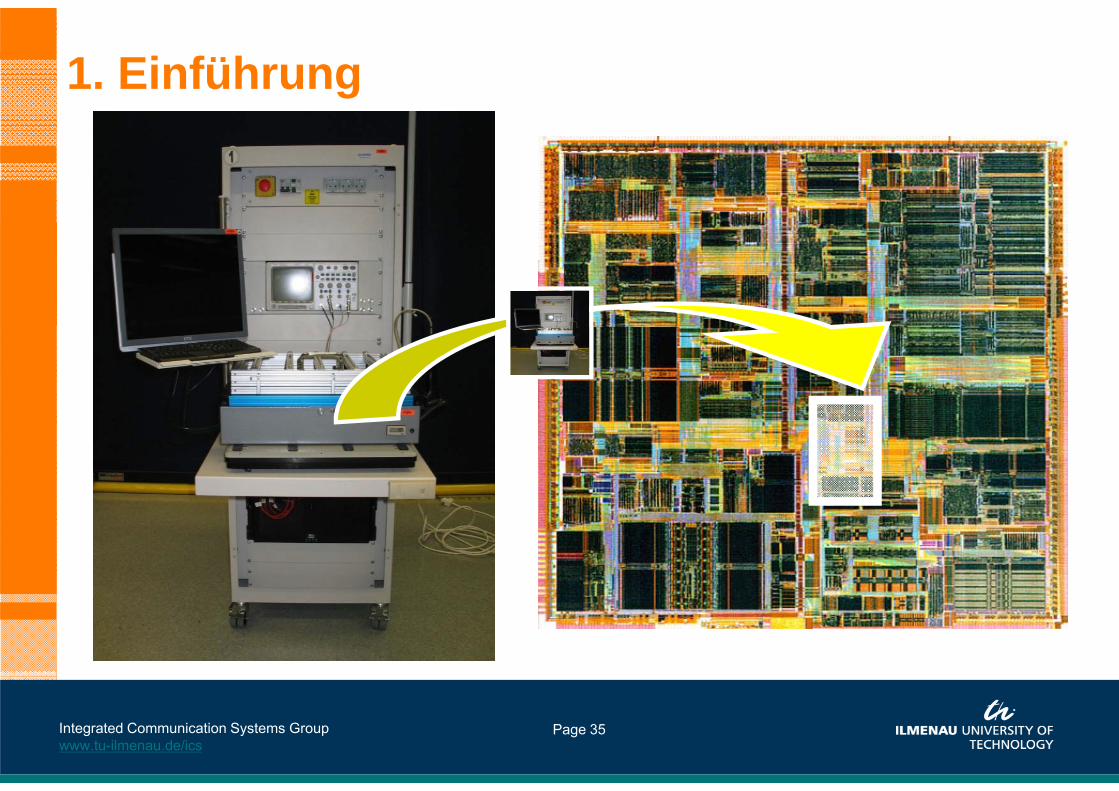
1. Einführung

Prof. Dr.-Ing. habil. Andreas Mitschele-ThielIntegrated HW/SW Systems Group
Self-Organization19 February 2014 36
Integrated Communication Systems Groupwww.tu-ilmenau.de/ics
Page 36
• Testprobleme steigen mit zunehmender Komplexität– Längere Testzeiten– Geringere Fehlerabdeckung:
ungetestete high-speed Module
• ERADOS Ziele– Verfügbare FPGAs zur
Beschleunigung des Testens– Algorithmenbeschleunigung durch
Verteilung– Verbesserung von Testzeit und
Fehlerabdeckung
1. Einführung: Motivation
Board with FPGA

Prof. Dr.-Ing. habil. Andreas Mitschele-ThielIntegrated HW/SW Systems Group
Self-Organization19 February 2014 37
Integrated Communication Systems Groupwww.tu-ilmenau.de/ics
Page 37
• BScan: klassisch– Alle Testfunktionen auf dem PC
• Testalgorithmus• Pattern Generation und Analyse• Ansteuerfunktionen der zu testenden Leiterplatte (DUT)
– JTAG Interface zur Ein-/ Ausgabe von Testwerten
1. Einführung: Stand der Technik
Prof. Dr.-Ing. habil. Andreas Mitschele-ThielIntegrated HW/SW Systems Group
Self-Organization19 February 2014 38
Integrated Communication Systems Groupwww.tu-ilmenau.de/ics
Page 38
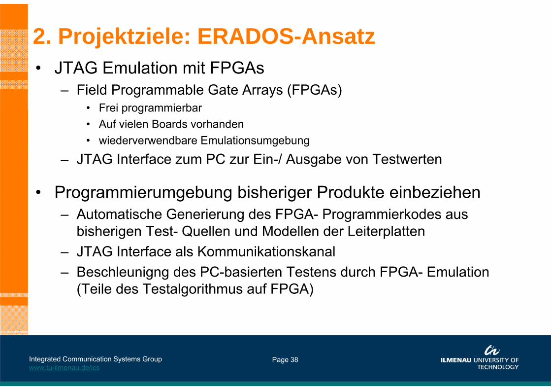
• JTAG Emulation mit FPGAs– Field Programmable Gate Arrays (FPGAs)
• Frei programmierbar• Auf vielen Boards vorhanden• wiederverwendbare Emulationsumgebung
– JTAG Interface zum PC zur Ein-/ Ausgabe von Testwerten
• Programmierumgebung bisheriger Produkte einbeziehen– Automatische Generierung des FPGA- Programmierkodes aus
bisherigen Test- Quellen und Modellen der Leiterplatten– JTAG Interface als Kommunikationskanal– Beschleunigng des PC-basierten Testens durch FPGA- Emulation
(Teile des Testalgorithmus auf FPGA)
2. Projektziele: ERADOS-Ansatz

Prof. Dr.-Ing. habil. Andreas Mitschele-ThielIntegrated HW/SW Systems Group
Self-Organization19 February 2014 39
Integrated Communication Systems Groupwww.tu-ilmenau.de/ics
Page 39
• BScan: Klassisch– Alle Testfunktionen auf dem PC
• Testalgorithms• Pattern Generation und Analyse• Ansteuerfunktionen der zu testenden
Leiterplatte (DUT)
– JTAG interface zur Ein-/ Ausgabe von Testwerten
• ERADOS test system– Testteile implementiert innerhalb
eines FPGA– JTAG Interface als
Kommunikationskanal
2. Projektziel: ERADOS Ansatz
BScan test environment
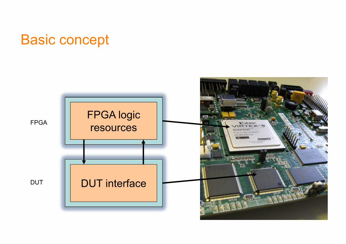
device under test(DUT)
device for test(DFT)
Basic concept
FPGA logicresources
DUT interface
FPGA
DUT

Basic conceptusual JTAG
FPGA logic resources DFT(FPGA)
DUT interfaceDUT
Pins

Basic conceptusual JTAG
FPGA logic resources
DUT interface
TDI
TDO
TAP
Con
trolle
r
DUT
DFT(FPGA)
BScan cells
BScan chain

TAP
Con
trolle
r
FPGA logic resources
010
Basic conceptusual JTAG
DUT interface
TDI
TDO
011101011001*0101
1
0101
DUT
DFT(FPGA)
Architecture of an Adaptive Test System Built on FPGAsPage 44
Integrated Communication Systems Groupwww.tu-ilmenau.de/ics
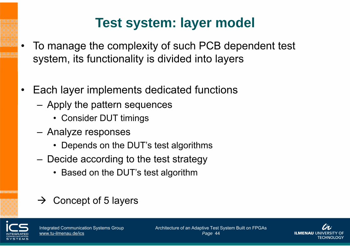
Test system: layer model• To manage the complexity of such PCB dependent test
system, its functionality is divided into layers
• Each layer implements dedicated functions– Apply the pattern sequences
• Consider DUT timings– Analyze responses
• Depends on the DUT’s test algorithms– Decide according to the test strategy
• Based on the DUT’s test algorithm
Concept of 5 layers

Architecture of an Adaptive Test System Built on FPGAsPage 45
Integrated Communication Systems Groupwww.tu-ilmenau.de/ics
Test system: layer model• L5: controls the whole test
procedure• L4: analyzes the test results
and decides the next test step
• L3: compares the result patterns with their expected values
• L2: dependent on the used test algorithm (shift-, count-rotate- or other special operations)
• L1: basic functions to access the device under test (read, write operation)
L5
L4
L3
L2
L1
Test ProgramMain Control
Test Analysis
TestComparator
DUT Test-Primitives
DUT Access-Primitives
Layer Stack

Architecture of an Adaptive Test System Built on FPGAsPage 46
Integrated Communication Systems Groupwww.tu-ilmenau.de/ics
Test system: layer model• Each of these layers can be implemented:
– In software running at the embedded test processor– Directly in HW as a co-processing units– In software running at the Test-PC
Optimization concerning available resources and needed performance
Bachelor, Master, PhD- Themes

Basic conceptERADOS layer 1
FPGA logic resources
DUT interface
TDI
TDO
TAP
Con
trolle
r*0101
1 0 1 0
1
DUT
DFT(FPGA)

FPGA logic resources
Basic conceptERADOS layer 2
DUT interface
TDI
TDO
TAP
Con
trolle
r*10
DUT
DFT(FPGA)
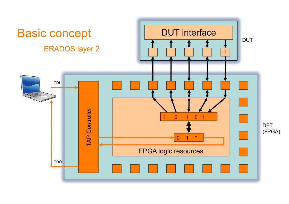
FPGA logic resources
Basic conceptERADOS layer 2
DUT interface
TDI
TDO
0 1
1
TAP
Con
trolle
r
1 0 1 0
1
0 1 *
DUT
DFT(FPGA)
FPGA logic resources
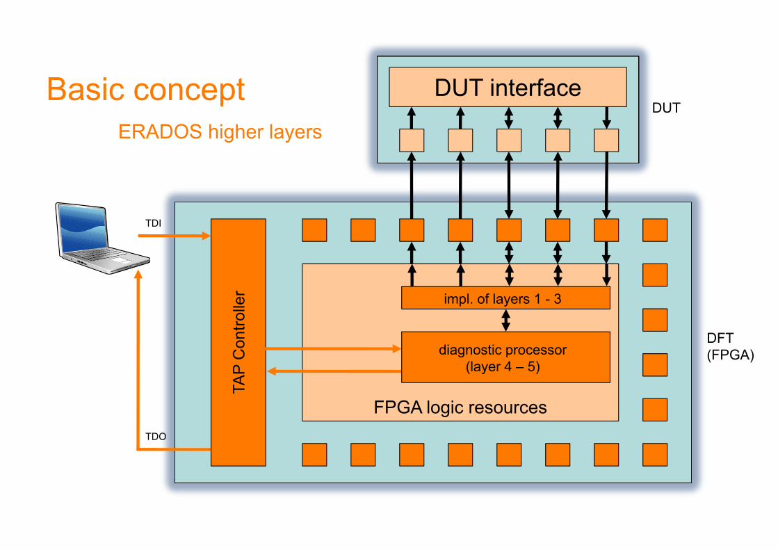
Basic conceptERADOS higher layers
DUT interface
TDI
TDO
TAP
Con
trolle
r impl. of layers 1 - 3
DUT
DFT(FPGA)diagnostic processor
(layer 4 – 5)

Architecture of an Adaptive Test System Built on FPGAsPage 51
Integrated Communication Systems Groupwww.tu-ilmenau.de/ics
Test system architecture Automation• Why?
– A must for real industrial test applications– Adaptability to unknown environment
• How?– Based on DUT-M, FPGA constraints, PCB and test cases– HW/SW partitioning– Layers implemented in hardware are transformed to their
hardware descriptions – Layers realized in software are transformed to object code

Prof. Dr.-Ing. habil. Andreas Mitschele-ThielIntegrated HW/SW Systems Group
Self-Organization19 February 2014 52
Integrated Communication Systems Groupwww.tu-ilmenau.de/ics
Page 52
4. Ergebnisse: Algorithmen-Integration
Automatic test system generation flow
• Eingaben– IP Blöcke– Ein-/ Ausgangs Information– DUT Modell
• Übersetzung – Informationsextraktion– Code Generierung
• Ergebnis– FPGA Programmierungs-Datei

Architecture of an Adaptive Test System Built on FPGAsPage 53
Integrated Communication Systems Groupwww.tu-ilmenau.de/ics
Test System Architecture DUT Models• Device model (DUT-M)
– Access functionality– Test algorithms– Parameters
• Bus width, package, pins, timing information, …
• L1 based on the DUT-M access functions and parameters
• L2-L5 functions based on the test algorithms and parameters
RAM DUT‐MADDRESS(PIN A0, A1, A2, .., A7)
DATA(PIN DQ0, DQ1, DQ2, .., DQ7)
CONTROL(PIN OE, WE, CE)
ACCESS FUNCTIONS(CYCLE WRITE [110], [100], [110])(CYCLE READ [110], [010], [110])(CYCLE OFF [111])
TEST1( ..... )
TEST2( ..... )
END DUT‐M
DUT-M example

Architecture of an Adaptive Test System Built on FPGAsPage 54
Integrated Communication Systems Groupwww.tu-ilmenau.de/ics
Implementation Test scenarioPrototype implementation

Prof. Dr.-Ing. habil. Andreas Mitschele-ThielIntegrated HW/SW Systems Group
Self-Organization19 February 2014 55
Integrated Communication Systems Groupwww.tu-ilmenau.de/ics
Page 55
4. Ergebnisse:
DUT Classic BSCAN Test Time (s)
Processor based Test SystemSpeed-up
Prog. Time (s) Test Time (s) Total (s)
SRAM 2 0.65 0.1 0.75 2.7LCD Display 120 0.65 7 7.65 15.6
Comparison table
• SRAM Verbindungstest Algorithmus Daten- und Adressbus Verbindungstest
• LCD Display Funktionstest Algorithmus Pixelgenerierung
Architecture of an Adaptive Test System Built on FPGAsPage 56
Integrated Communication Systems Groupwww.tu-ilmenau.de/ics
ROBSY-project (2011-2013Re-konfigurierbares On Board Selbsttest-SYstem
Architecture of an Adaptive Test System Built on FPGAsPage 57
Integrated Communication Systems Groupwww.tu-ilmenau.de/ics
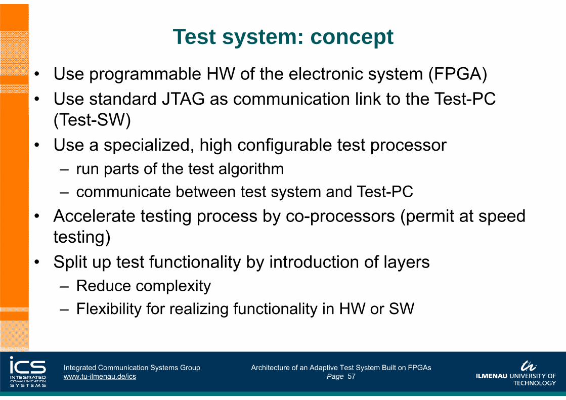
Test system: concept• Use programmable HW of the electronic system (FPGA)• Use standard JTAG as communication link to the Test-PC
(Test-SW)• Use a specialized, high configurable test processor
– run parts of the test algorithm – communicate between test system and Test-PC
• Accelerate testing process by co-processors (permit at speed testing)
• Split up test functionality by introduction of layers– Reduce complexity– Flexibility for realizing functionality in HW or SW

Architecture of an Adaptive Test System Built on FPGAsPage 58
Integrated Communication Systems Groupwww.tu-ilmenau.de/ics
Test system: concept• Interfaces
– IEEE 1149.1– Peripherals (DUTs)
• Processor– Communication with host PC
and co-processors– In charge of the execution flow– Boolean/integer arithmetic– Interrupt handling
• Co-processors – Accelerate test execution DUT1
. . .
FPGA
JTAG
Co-proc Co-proc
Processor
Co-proc
DUT2 DUTn

Architecture of an Adaptive Test System Built on FPGAsPage 59
Integrated Communication Systems Groupwww.tu-ilmenau.de/ics
Test system: modeling language• Hardware related, test oriented modeling language (DSL) to
describe the DUT’s:
– Interface• Data, address, control bus
– Timing (L1)– Device functions (L1)
• Read, write cycle– Test algorithm(s)
• L2 .. L4: procedures• L5: main program
DATA (...)ADDRESS (...)CONTROL (...)
INTERFACE (
)
...
PROGRAM prog (...)BEGIN
END.
L2: PROCEDURE proc1 (...)BEGIN
END...
CYCLE writeBEGIN
END...
...
VAR i1, i2, xyz;
TIMING (...)
MODULE mod1 (...)

Architecture of an Adaptive Test System Built on FPGAsPage 60
Integrated Communication Systems Groupwww.tu-ilmenau.de/ics
Test system: generation• HW/SW partitioning
– Based on the DUT model’s timing section, test algorithm, and PCB properties
– Depends on the required performance and available resources
• Layers realized in SW– Model transformation to test processor object code– Model transformation to SW code executed at the Test-PC
• Layers implemented in HW– Model transformation to a hardware description (VHDL)

Architecture of an Adaptive Test System Built on FPGAsPage 61
Integrated Communication Systems Groupwww.tu-ilmenau.de/ics
Test system: architecture• Control and Debug IF
– Communication port to thehost PC
– Load/change program code– Read/write internal registers
• Processor– Run complex algorithms
• Bus system– Processor co-processor link
• Co-processors– HW accelerators– Meet timing constraints
FPGA
JTAG
Control-Debug IF
Processor
Bus
IRQ
DUT1 DUT2 DUTn. . .. . .Co-proc Co-procCo-proc
Architecture of an Adaptive Test System Built on FPGAsPage 62
Integrated Communication Systems Groupwww.tu-ilmenau.de/ics
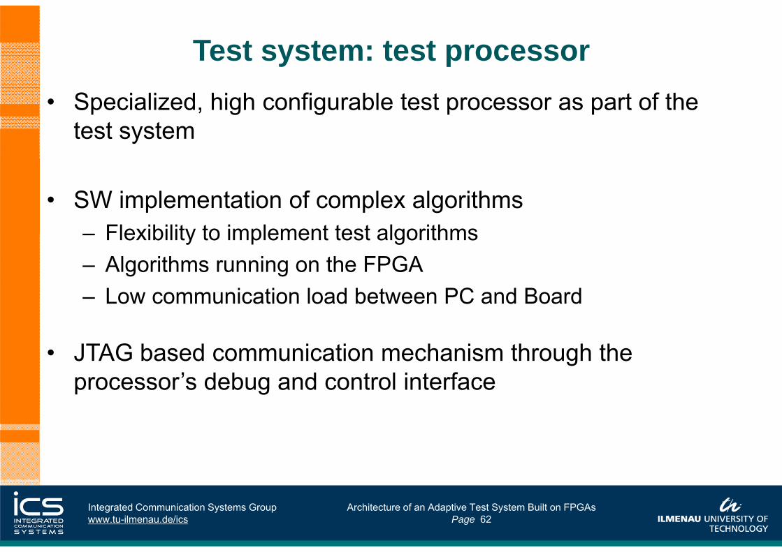
Test system: test processor• Specialized, high configurable test processor as part of the
test system
• SW implementation of complex algorithms– Flexibility to implement test algorithms– Algorithms running on the FPGA– Low communication load between PC and Board
• JTAG based communication mechanism through the processor’s debug and control interface

Architecture of an Adaptive Test System Built on FPGAsPage 63
Integrated Communication Systems Groupwww.tu-ilmenau.de/ics
Test system: test processor• Harvard architecture• Single instruction
single data (SISD)• Reduced instruction
set computer (RISC)
• Program Memory: 4kx18• Stack Memory: 1kx18• Data Memory: 2kx8• External bus: 31kx8
(Wishbone)
CPU
JumpTarget
StateMachine ALU Int/Exc
Modules
StackInterface
DataMultiplexer
ProgramMemory
StackMemory
DataMemory
Control and Debug IF
Wis
hbon
e IF
Proc
esso
r
Architecture of an Adaptive Test System Built on FPGAsPage 64
Integrated Communication Systems Groupwww.tu-ilmenau.de/ics
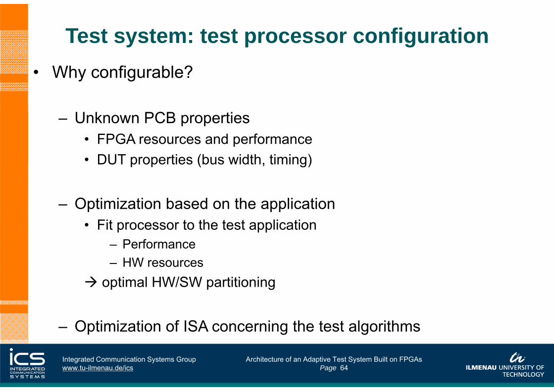
Test system: test processor configuration• Why configurable?
– Unknown PCB properties• FPGA resources and performance• DUT properties (bus width, timing)
– Optimization based on the application• Fit processor to the test application
– Performance– HW resources
optimal HW/SW partitioning
– Optimization of ISA concerning the test algorithms

Architecture of an Adaptive Test System Built on FPGAsPage 65
Integrated Communication Systems Groupwww.tu-ilmenau.de/ics
Test system: test processor configuration• Configuration of the pre-defined architecture
– Memory sizes• Program, data, stack memory
– Number of registers– Data path width– External bus parameters (Wishbone bus)– Enable/disable instructions
• Extend the processor– Addition of special instructions

Prof. Dr.-Ing. habil. Andreas Mitschele-ThielIntegrated HW/SW Systems Group
Self-Organization19 February 2014 66
Integrated Communication Systems Groupwww.tu-ilmenau.de/ics
Page 66
ROBSY: Testsystem auf FPGA
Possible test environment

Architecture of an Adaptive Test System Built on FPGAsPage 67
Integrated Communication Systems Groupwww.tu-ilmenau.de/ics
Conclusion • Test system supplies the benefits known from emulators to all
PCBs containing an FPGA• Adaptability due to DUT models• Co-processors permit at speed testing
• Technology independent concept– Test system can be implemented on FPGAs of different vendors
and families• Maintaining the standard JTAG interface as communication
link– Seamless integration in existing test tools– No additional HW required for testing