ihs 3: test of digital systems fileintegrierte hard- und softwaresysteme ihs 3: test of digital...
TRANSCRIPT
Integrierte Hard- und Softwaresysteme
IHS 3: Test of Digital Systems
R.Ubar, A. Jutman, H-D. Wuttke
Technical University Tallinn, ESTONIACopyright 2000-2003 by Raimund Ubar
2
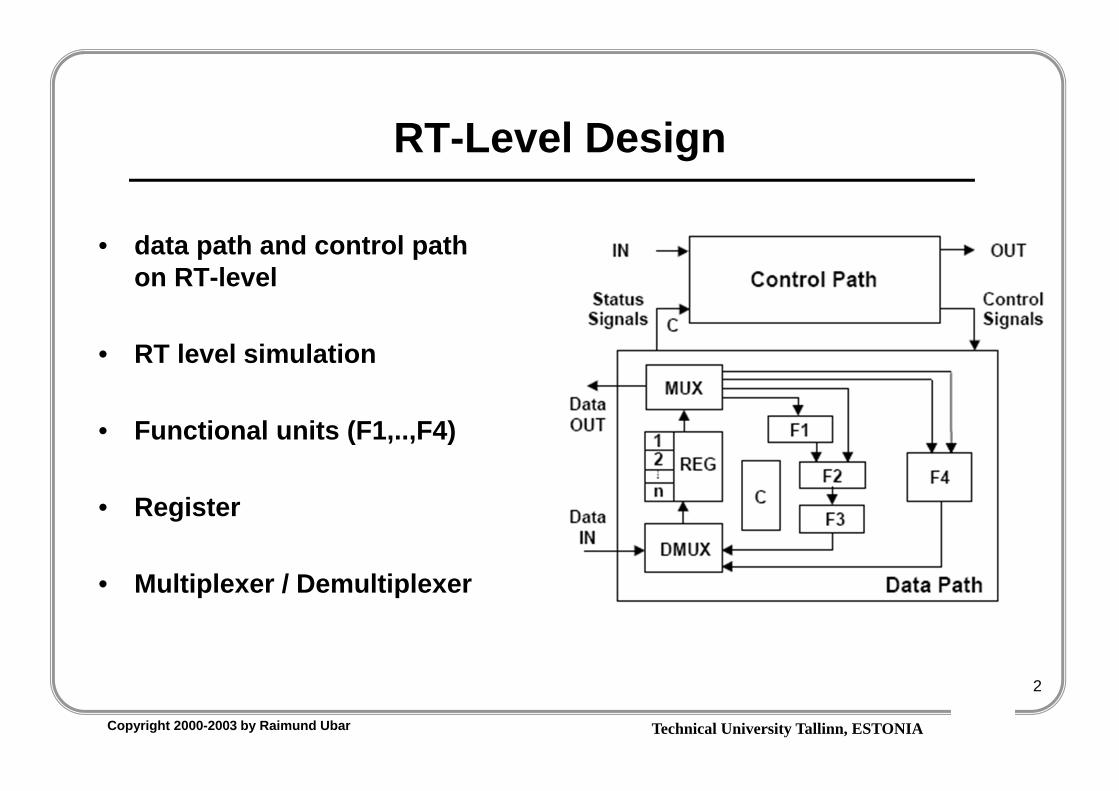
RT-Level Design
• data path and control path on RT-level
• RT level simulation
• Functional units (F1,..,F4)
• Register
• Multiplexer / Demultiplexer
Technical University Tallinn, ESTONIACopyright 2000-2003 by Raimund Ubar
3
Fault Modeling on High Level DDsHigh-level DDs (RT-level):
R2M3
e+M1
a
*M2
b
R1
IN
c
d
y1 y2 y3 y4
y4
y3 y1 R1 + R2
IN + R2
R1* R2
IN* R2
y2
R2 0
1
2 0
1
0
1
0
1
0
R2
IN
R12
3
2
M1
y1 Function0 M1 = R1
1 M1 = INM2
y2 Function0 M2 = R1
1 M2 = INM3
y3 Function0 M3 = M1+ R2
1 M3 = IN2 M3 = R1
3 M3= M2* R2
R2
y4 Operation Function0 Reset R2 = 01 Hold R2 = R’2
Load R2 = M3
Technical University Tallinn, ESTONIACopyright 2000-2003 by Raimund Ubar
4
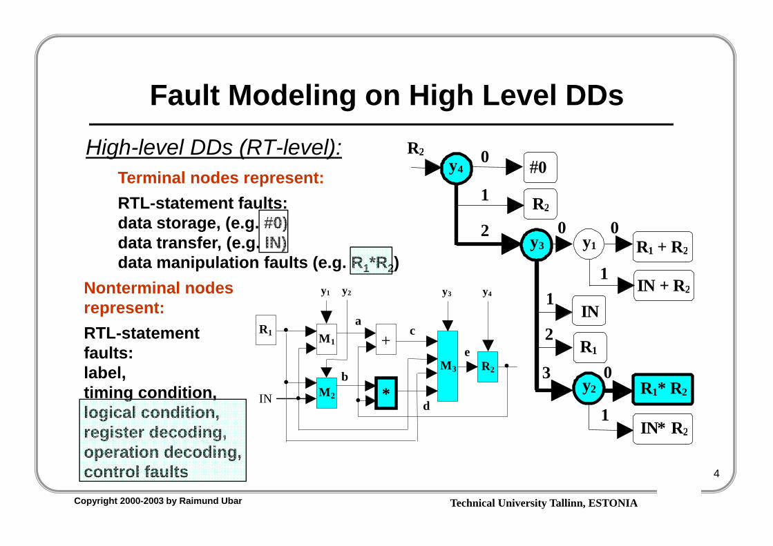
Fault Modeling on High Level DDsHigh-level DDs (RT-level):
R2M3
e+M1
a
*M2
b
R1
IN
c
d
y1 y2 y3 y4
y4
y3 y1 R1 + R 2 IN + R 2
R1* R 2 IN* R 2
y2
R2 0
1
2 0
1
0
1
0
1
0
R2
IN
R12
3
Terminal nodes represent:RTL-statement faults: data storage, (e.g. #0)data transfer, (e.g. IN)data manipulation faults (e.g. R1*R2)
Nonterminal nodesrepresent: RTL-statement faults: label, timing condition, logical condition, register decoding, operation decoding,control faults
Technical University Tallinn, ESTONIACopyright 2000-2003 by Raimund Ubar
5
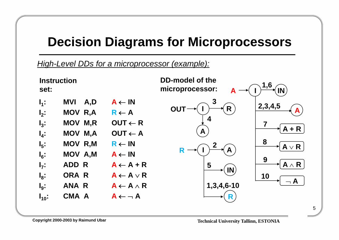
Decision Diagrams for Microprocessors
I1: MVI A,D A INI2: MOV R,A R AI3: MOV M,R OUT RI4: MOV M,A OUT AI5: MOV R,M R INI6: MOV A,M A INI7: ADD R A A + RI8: ORA R A A RI9: ANA R A A RI10: CMA A A A
High-Level DDs for a microprocessor (example):
Instruction set:
3I R
A
OUT4
I A2R
IN5
R1,3,4,6-10
I IN1,6
A
A2,3,4,5
A + R7
A R8
A R9
A10
DD-model of themicroprocessor:
Technical University Tallinn, ESTONIACopyright 2000-2003 by Raimund Ubar
6
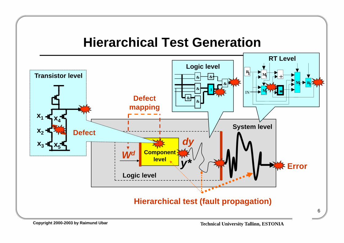
Componentlevel
dy
Defect mapping
Hierarchical Test Generation
System level
Wd
Logic levelError
Hierarchical test (fault propagation)
y*
&
&
&
1
&
&
&
Logic level
R2M3
+M1
*M2
R1
IN
RT Level
x1
x2
x3
x4
x5
Defect
Transistor level
Technical University Tallinn, ESTONIACopyright 2000-2003 by Raimund Ubar
7
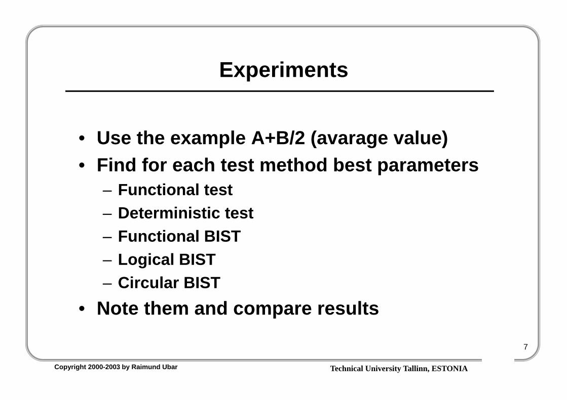
Experiments
• Use the example A+B/2 (avarage value)• Find for each test method best parameters
– Functional test– Deterministic test– Functional BIST– Logical BIST– Circular BIST
• Note them and compare results

Technical University Tallinn, ESTONIACopyright 2000-2003 by Raimund Ubar
8
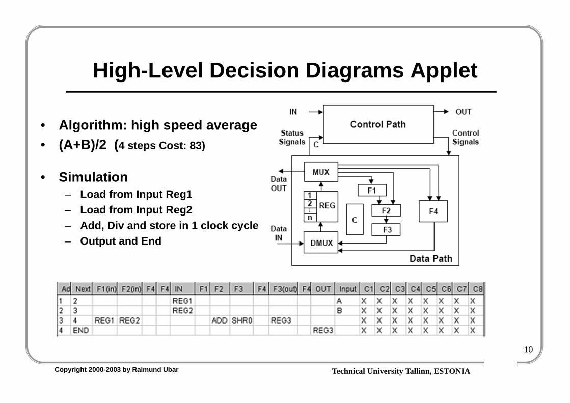
High-Level Decision Diagrams Applet
• Algorithm: average• (A+B)/2
• a) high speed– 2 operation units (F2, F3)– Add and Div in in 1 clock cycle– 4 steps– Cost: 83

Technical University Tallinn, ESTONIACopyright 2000-2003 by Raimund Ubar
9
High-Level Decision Diagrams Applet
• Algorithm: average• (A+B)/2
• b) low cost– Only 1 Unit (F4)– 2 clock cycles for operation– 5 clocks – Cost: 73
Technical University Tallinn, ESTONIACopyright 2000-2003 by Raimund Ubar
10
High-Level Decision Diagrams Applet
• Algorithm: high speed average• (A+B)/2 (4 steps Cost: 83)
• Simulation– Load from Input Reg1– Load from Input Reg2– Add, Div and store in 1 clock cycle– Output and End

Technical University Tallinn, ESTONIACopyright 2000-2003 by Raimund Ubar
11
Applets for Learning RT- Level Test
Functional Test mode:The test vectors are operands results can be observed at the output, no extra test parts
Deterministic Test mode:Gate level test for each FU separatly, generate test vectors, local test panel, cumulative FC calculation
BIST mode:Functional-, Logical- Circular Built In Self Test via extra test part: Test Pattern Generator and Signature analyzer
Technical University Tallinn, ESTONIACopyright 2000-2003 by Raimund Ubar
12
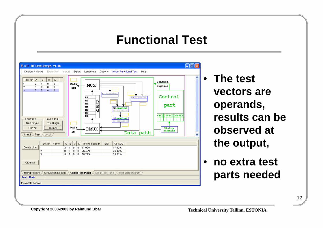
Functional Test
• The test vectors areoperands, results can be observed at the output,
• no extra test parts needed

Technical University Tallinn, ESTONIACopyright 2000-2003 by Raimund Ubar
13
High-Level Decision Diagrams Applet
• Algorithm: average• (A+B)/2
• Funct.• Test

Technical University Tallinn, ESTONIACopyright 2000-2003 by Raimund Ubar
14
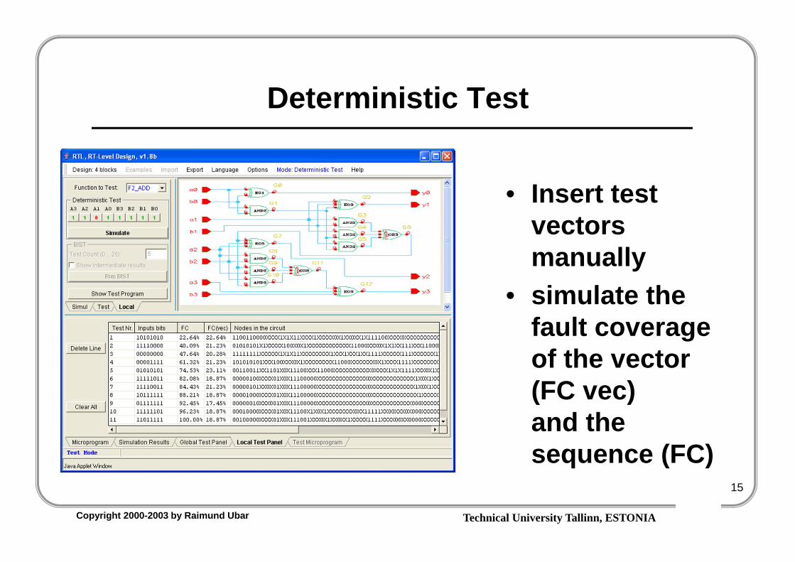
Deterministic Test
• Adder (F2)– Schematic level– Gate level test– Boolean derivation– SSBDDs– Path activation– Fault propagation– Fault observation
Technical University Tallinn, ESTONIACopyright 2000-2003 by Raimund Ubar
15
Deterministic Test
• Insert test vectors manually
• simulate the fault coverage of the vector (FC vec) and the sequence (FC)

Technical University Tallinn, ESTONIACopyright 2000-2003 by Raimund Ubar
16
Overview
1. Introduction2. Theory: Boolean differential algebra3. Theory: Decision diagrams4. Fault modelling5. Test generation6. Fault simulation7. Fault diagnosis8. Testability measuring9. Design for testability
10.Built in Self-Test
Technical University Tallinn, ESTONIACopyright 2000-2003 by Raimund Ubar
17
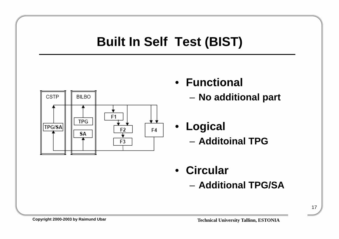
Built In Self Test (BIST)
• Functional– No additional part
• Logical– Additoinal TPG
• Circular– Additional TPG/SA
Technical University Tallinn, ESTONIACopyright 2000-2003 by Raimund Ubar
18
Built-In Self-Test
• Motivations for BIST:– Need for a cost-efficient testing– Doubts about the stuck-at fault model– Increasing difficulties with TPG (Test Pattern Generation)– Growing volume of test pattern data– Cost of ATE (Automatic Test Equipment)– Test application time– Gap between tester and UUT (Unit Under Test) speeds
• Drawbacks of BIST:– Additional pins and silicon area needed– Decreased reliability due to increased silicon area– Performance impact due to additional circuitry– Additional design time and cost

Technical University Tallinn, ESTONIACopyright 2000-2003 by Raimund Ubar
19
Built-In Self-Test in SoC
SoC
SRAMPeripherial ComponentInterconnect
SRAM
CPU
Wrapper
CoreUnderTest
ROM
MPEG UDLDRAM
Test AccessMechanism
Test AccessMechanism
Source
Sink
System-on-Chip testing Test architecture components:• Test pattern source & sink• Test Access Mechanism• Core test wrapper
Solutions:• Off-chip solution
– need for external ATE• Combined solution
– mostly on-chip, ATE needed for control
• On-chip solution– BIST

Technical University Tallinn, ESTONIACopyright 2000-2003 by Raimund Ubar
20
Built-In Self-Test Components
BIST Control Unit
Circuitry Under Test
CUT
Test Pattern Generation (TPG)
Test Response Analysis (TRA)
• BIST components:– Test pattern generator
(TPG)– Test response
analyzer (TRA)• TPG & TRA are usually
implemented as linear feedback shift registers (LFSR)
• Two widespread schemes:
– test-per-scan– test-per-clock

Technical University Tallinn, ESTONIACopyright 2000-2003 by Raimund Ubar
21
Linear Feedback Shift Register (LFSR)
Pseudorandom Test generation by LFSR:
1 x x2
x3
x4
x2 x 1x4
x3
Polynomial: P(x) = 1 + x3 + x4
Standard LFSR
Modular LFSR

Technical University Tallinn, ESTONIACopyright 2000-2003 by Raimund Ubar
22
LFSR
• Find configurations of the LSFR – (Linear Feedback
Shift Register) that generates optimal test vektors (TPG/SA)
• Parameters: – Feedback polynom – Initial State

Technical University Tallinn, ESTONIACopyright 2000-2003 by Raimund Ubar
23
LFSR: Signature Analyser
1 x x2 x3 x4
LFSR
UUT
Response string for Signature Analysis
Test Patterns (when generating tests)Signature (when analyzing test responses)
FF FF FF FF
Stimuli
Technical University Tallinn, ESTONIACopyright 2000-2003 by Raimund Ubar
24
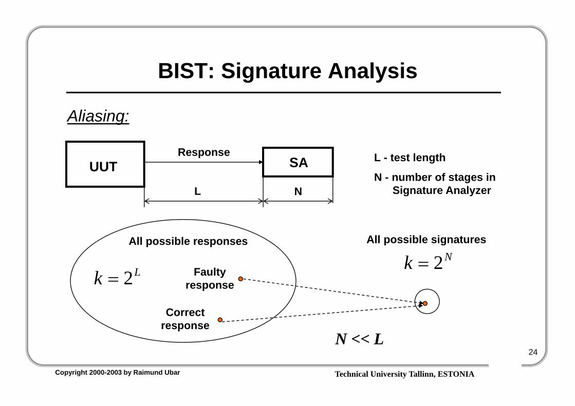
BIST: Signature Analysis
Aliasing:
UUTResponse
SA
L N
L - test length
N - number of stages inSignature Analyzer
Lk 2
All possible responses All possible signaturesNk 2Faulty
response
Correct response
N << L

Technical University Tallinn, ESTONIACopyright 2000-2003 by Raimund Ubar
25
BIST: Signature Analysis
• TPG / SA– Registers
for LFSR• Configure
– Initial state– Polynom
• Parameters– TPG LFSR– SA LFSR

Technical University Tallinn, ESTONIACopyright 2000-2003 by Raimund Ubar
26
BIST: Signature Analysis
Aliasing:
UUTResponse
SA
L N
L - test length
N - number of stages inSignature Analyzer
Lk 2 - number of different possible responses
No aliasing is possible for those strings with L - N leading zeros since they are represented by polynomials of degree N - 1 that are not divisible
by characteristic polynomial of LFSR. There are such stringsNL2Probability of aliasing:
1212
L
NL
P NP 211L
N << L
Technical University Tallinn, ESTONIACopyright 2000-2003 by Raimund Ubar
27
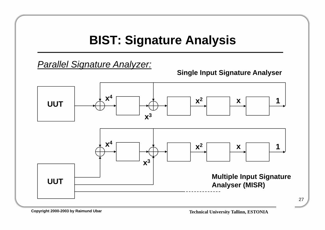
BIST: Signature Analysis
x2 x 1x4
x3
Parallel Signature Analyzer:
UUT
x2 x 1x4
x3
UUT Multiple Input Signature Analyser (MISR)
Single Input Signature Analyser

Technical University Tallinn, ESTONIACopyright 2000-2003 by Raimund Ubar
28
Built-In Self-Test
Signature calculating for multiple outputs:
LFSR - Test Pattern Generator
Combinational circuit
LFSR - Signature analyzer
Multiplexer
LFSR - Test Pattern Generator
Combinational circuit
LFSR - Signature analyzer
Multiplexer

Technical University Tallinn, ESTONIACopyright 2000-2003 by Raimund Ubar
29
Test-per-Clock BIST Architectures
BILBO - Built- In Logic Block Observer:
CSTP - Circular Self-Test Path:
LFSR - Test Pattern Generator
Combinational circuit
LFSR - Signature analyzer
LFSR - Test Pattern Generator
& Signature analyser
Combinational circuit

Technical University Tallinn, ESTONIACopyright 2000-2003 by Raimund Ubar
30
Reconfiguration for Self-Test
Module
R
Scan-IN
Scan-OUT
R
Module
Pseudorandom test generator
Signature AnalyserTest controller
Technical University Tallinn, ESTONIACopyright 2000-2003 by Raimund Ubar
31
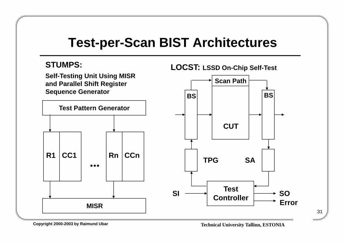
Test-per-Scan BIST Architectures
Test Pattern Generator
MISR
R1 CC1...
STUMPS:Self-Testing Unit Using MISR and Parallel Shift Register Sequence Generator
LOCST: LSSD On-Chip Self-Test
Rn CCn
Error
Test ControllerSI SO
TPG SA
CUT
BS BS
Scan Path
Technical University Tallinn, ESTONIACopyright 2000-2003 by Raimund Ubar
32
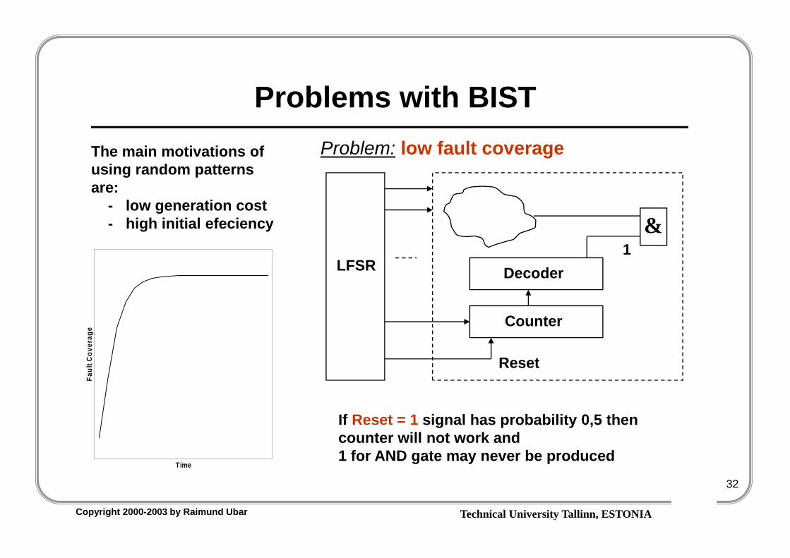
Problems with BIST
Time
Faul
t Cov
erag
e
Problem: low fault coverageThe main motivations of using random patterns are:
- low generation cost- high initial efeciency
Counter
Decoder
&
LFSR
Reset
If Reset = 1 signal has probability 0,5 then counter will not work and 1 for AND gate may never be produced
1

Technical University Tallinn, ESTONIACopyright 2000-2003 by Raimund Ubar
33
Problems with BIST
Time
Faul
t Cov
erag
e
Problem: low fault coverageThe main motivations of using random patterns are:
- low generation cost- high initial efeciency
0 2n-1
Possible patterns from LFSR: Pseudorandom
test:
Hard to test faults
0 2n-1Dream solution: find LFSR so that:

Technical University Tallinn, ESTONIACopyright 2000-2003 by Raimund Ubar
34
Store-and-Generate test architecture
Time
Faul
t Cov
erag
e
Problem: low fault coverageThe main motivations of using random patterns are:
- low generation cost- high initial efeciency
0 2n-1
Using many seeds:Pseudorandom test:
Hard to test faults
0 2n-1
Long PR test:Pseudorandom test:

Technical University Tallinn, ESTONIACopyright 2000-2003 by Raimund Ubar
35
Store-and-Generate test architecture
• ROM contains test patterns for hard-to-test faults • Each pattern Pk in ROM serves as an initial state of the LFSR for test pattern
generation (TPG)• Counter 1 counts the number of pseudorandom patterns generated starting
from Pk• After finishing the cycle for Counter 2 is incremented for reading the next
pattern Pk+1
ROM TPG UUT
ADR
Counter 2 Counter 1
RD
CL
Technical University Tallinn, ESTONIACopyright 2000-2003 by Raimund Ubar
36
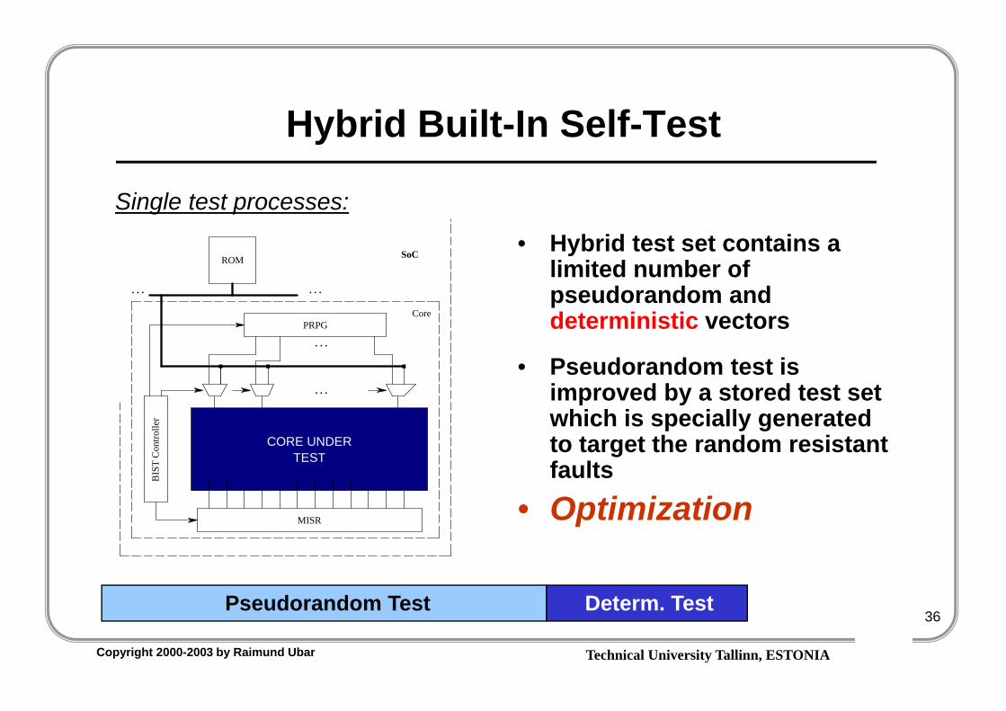
Hybrid Built-In Self-Test
PRPG
CORE UNDERTEST
. . .. . .
. . .
ROM
. . . . . .
SoC
Core
MISR
BIS
T C
ontro
ller
• Hybrid test set contains a limited number of pseudorandom and deterministic vectors
• Pseudorandom test is improved by a stored test set which is specially generated to target the random resistant faults
• Optimization
Single test processes:
Pseudorandom Test Determ. Test

Technical University Tallinn, ESTONIACopyright 2000-2003 by Raimund Ubar
37
Hybrid BIST for Multiple Cores
SoC
C3540
C1908 C880 C1355
Embedded Tester C2670
Test accessmechanismBIST BIST
BISTBISTBIST
Test Controller
TesterMemory
Embedded tester for testing multiple cores
Technical University Tallinn, ESTONIACopyright 2000-2003 by Raimund Ubar
38
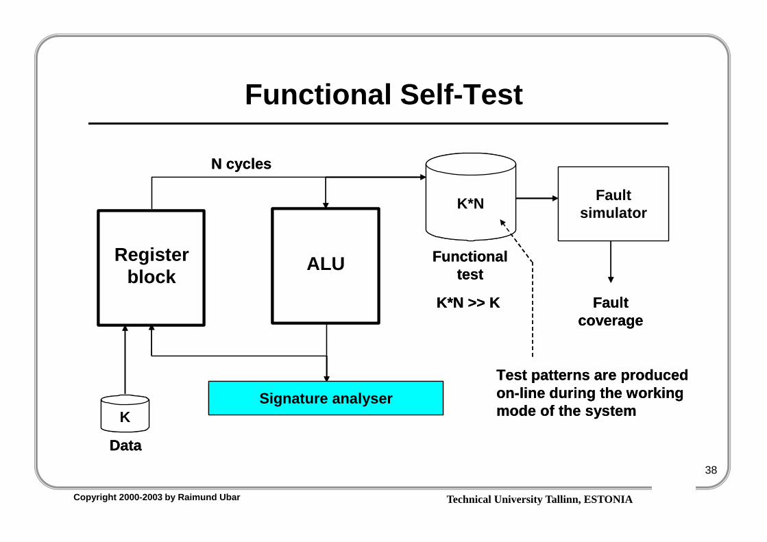
Functional Self-Test
Register block
ALU
Signature analyser
Functionaltest
Data
K
N cycles
K*N
K*N >> K
Fault simulator
Faultcoverage
Test patterns are produced on-line during the working mode of the system
Register block
ALU
Signature analyser
Functionaltest
Data
K
N cycles
K*N
K*N >> K
Fault simulator
Faultcoverage
Test patterns are produced on-line during the working mode of the system
Technical University Tallinn, ESTONIACopyright 2000-2003 by Raimund Ubar
39
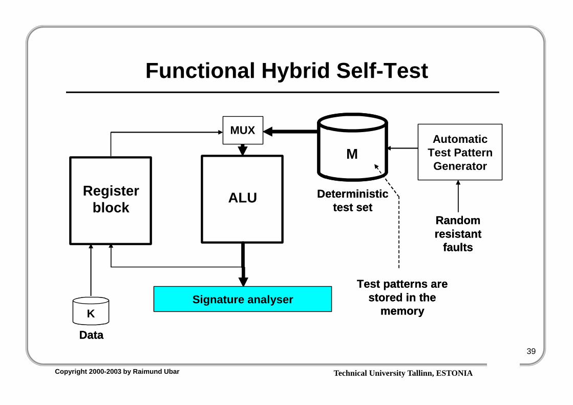
Functional Hybrid Self-Test
Register block
ALU
Signature analyser
Deterministictest set
Data
K
M Automatic
Test Pattern Generator
Randomresistant
faults
Test patterns are stored in the
memory
MUX
Register block
ALU
Signature analyser
Deterministictest set
Data
K
M Automatic
Test Pattern Generator
Randomresistant
faults
Test patterns are stored in the
memory
MUX

Technical University Tallinn, ESTONIACopyright 2000-2003 by Raimund Ubar
40
TURBO-TESTER: Low-Level TPG Tools
Test Generation
BIST Simulation
Methods:DeterministicRandomGenetic
Methods:BILBOCSTPStore/Generate
Design Test
Levels:GateMacro
Fault Simulation
Methods:Single faultParallelDeductive
Fault Table
Fault models:Stuck-at-faultsStuck-opensDelay faults
Test Optimization
Fault Diagnosis
Fault Location
http://www.pld.ttu.ee/tt/

Technical University Tallinn, ESTONIACopyright 2000-2003 by Raimund Ubar
41
Overview
1. Introduction2. Theory: Boolean differential algebra3. Theory: Decision diagrams4. Fault modelling5. Test generation6. Fault simulation7. Fault diagnosis8. Testability measuring
9. Design for testability10. Built in Self-Test

Technical University Tallinn, ESTONIACopyright 2000-2003 by Raimund Ubar
42
Ad Hoc Design for Testability TechniquesMethod of Test Points:
Block 1 Block 2Block 1 is not observable,Block 2 is not controllable
Block 1 Block 21- controllability:CP = 0 - normal working modeCP = 1 - controlling Block 2
with signal 1
1
CP
Improving controllability and observability:
Block 1 Block 20- controllability:CP = 1 - normal working modeCP = 0 - controlling Block 2
with signal 0
&
CP
OP
OP

Technical University Tallinn, ESTONIACopyright 2000-2003 by Raimund Ubar
43
Ad Hoc Design for Testability Techniques
• Find – good additional
observation points that improves the fault Coverage (FC)
• Find – optimal operands
(= test vektors)• Parameters:
– Observation points– Operands
Technical University Tallinn, ESTONIACopyright 2000-2003 by Raimund Ubar
44
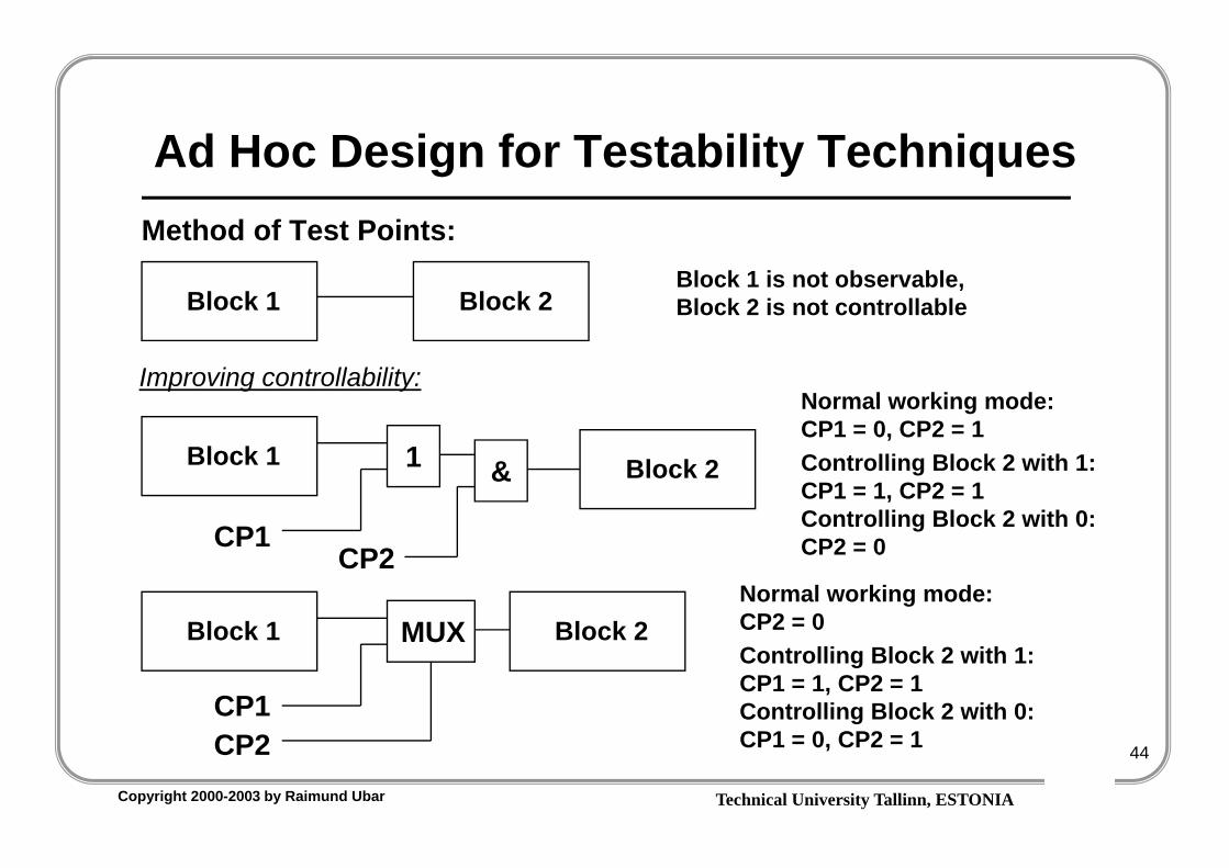
Ad Hoc Design for Testability TechniquesMethod of Test Points:
Block 1 Block 2Block 1 is not observable,Block 2 is not controllable
Block 1 Block 21
CP1
Improving controllability:
Block 1 Block 2
Normal working mode:CP1 = 0, CP2 = 1 Controlling Block 2 with 1:CP1 = 1, CP2 = 1Controlling Block 2 with 0:CP2 = 0
MUX
CP1
&
CP2
CP2
Normal working mode:CP2 = 0 Controlling Block 2 with 1:CP1 = 1, CP2 = 1Controlling Block 2 with 0:CP1 = 0, CP2 = 1
Technical University Tallinn, ESTONIACopyright 2000-2003 by Raimund Ubar
45
Ad Hoc Design for Testability Techniques
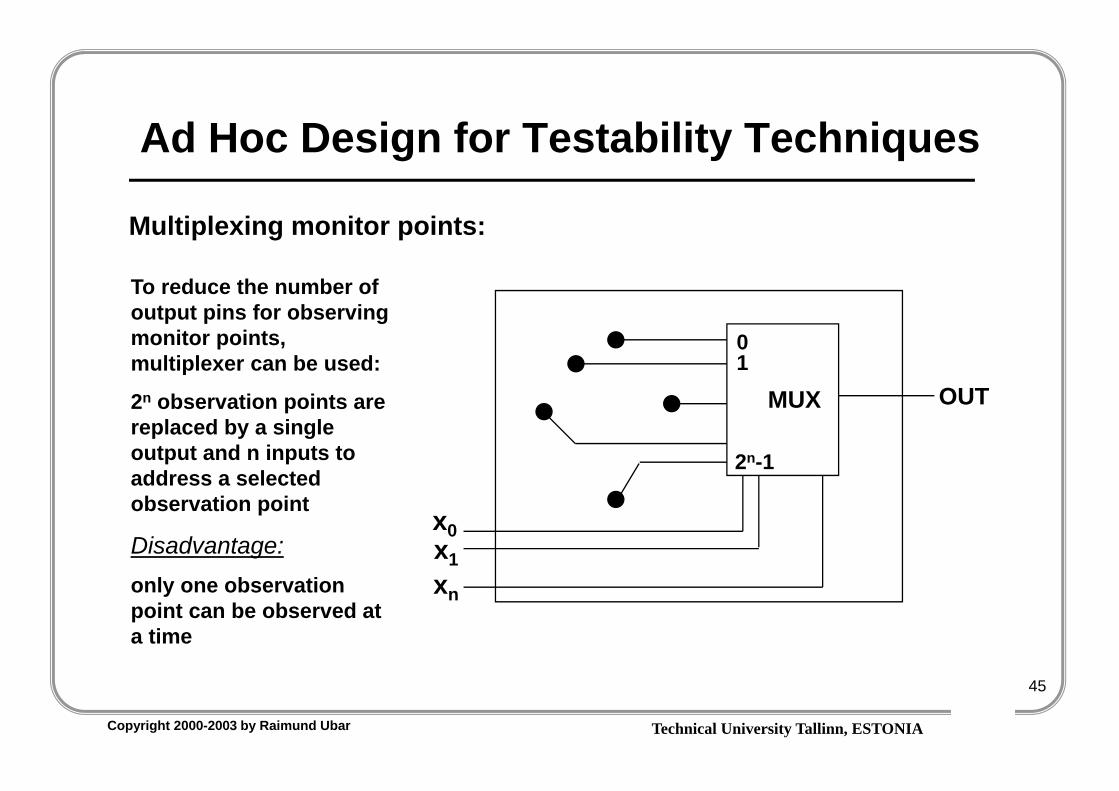
Multiplexing monitor points:
OUT
01
2n-1
x0
xn
x1
MUX
To reduce the number of output pins for observing monitor points, multiplexer can be used:
2n observation points are replaced by a single output and n inputs to address a selected observation point
Disadvantage:only one observation point can be observed at a time
Technical University Tallinn, ESTONIACopyright 2000-2003 by Raimund Ubar
46
Ad Hoc Design for Testability Techniques
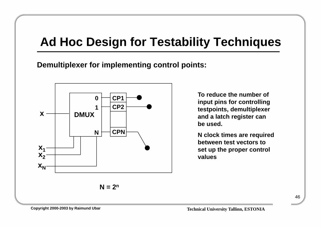
Demultiplexer for implementing control points:
01
N
DMUX
To reduce the number of input pins for controlling testpoints, demultiplexer and a latch register can be used.
N clock times are required between test vectors to set up the proper control values
x
CP1CP2
CPN
N = 2n
x1x2xN
Technical University Tallinn, ESTONIACopyright 2000-2003 by Raimund Ubar
47
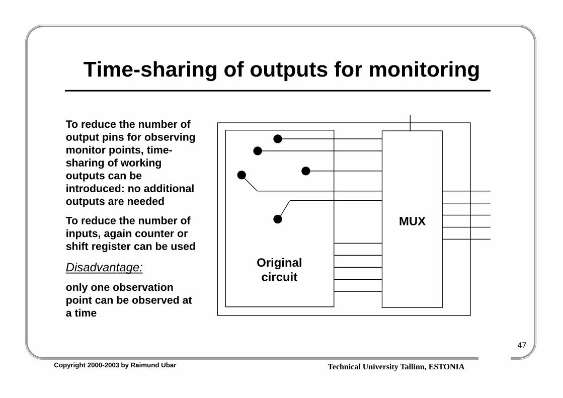
Time-sharing of outputs for monitoring
To reduce the number of output pins for observing monitor points, time-sharing of working outputs can be introduced: no additional outputs are needed
To reduce the number of inputs, again counter or shift register can be used
Disadvantage:only one observation point can be observed at a time
Original circuit
MUX
Technical University Tallinn, ESTONIACopyright 2000-2003 by Raimund Ubar
48
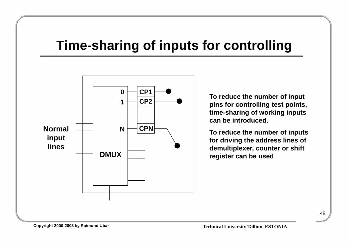
Time-sharing of inputs for controlling
01
N
DMUX
CP1CP2
CPN
To reduce the number of input pins for controlling test points, time-sharing of working inputs can be introduced.
To reduce the number of inputs for driving the address lines of demultiplexer, counter or shift register can be used
Normal input lines
Technical University Tallinn, ESTONIACopyright 2000-2003 by Raimund Ubar
49
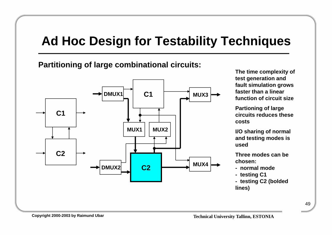
Ad Hoc Design for Testability Techniques
Partitioning of large combinational circuits:
C1
C2
DMUX1 C1
MUX1 MUX2
DMUX2 C2
MUX3
MUX4
The time complexity of test generation and fault simulation grows faster than a linear function of circuit size
Partioning of large circuits reduces these costs
I/O sharing of normal and testing modes is used
Three modes can be chosen: - normal mode - testing C1 - testing C2 (bolded lines)
Technical University Tallinn, ESTONIACopyright 2000-2003 by Raimund Ubar
50
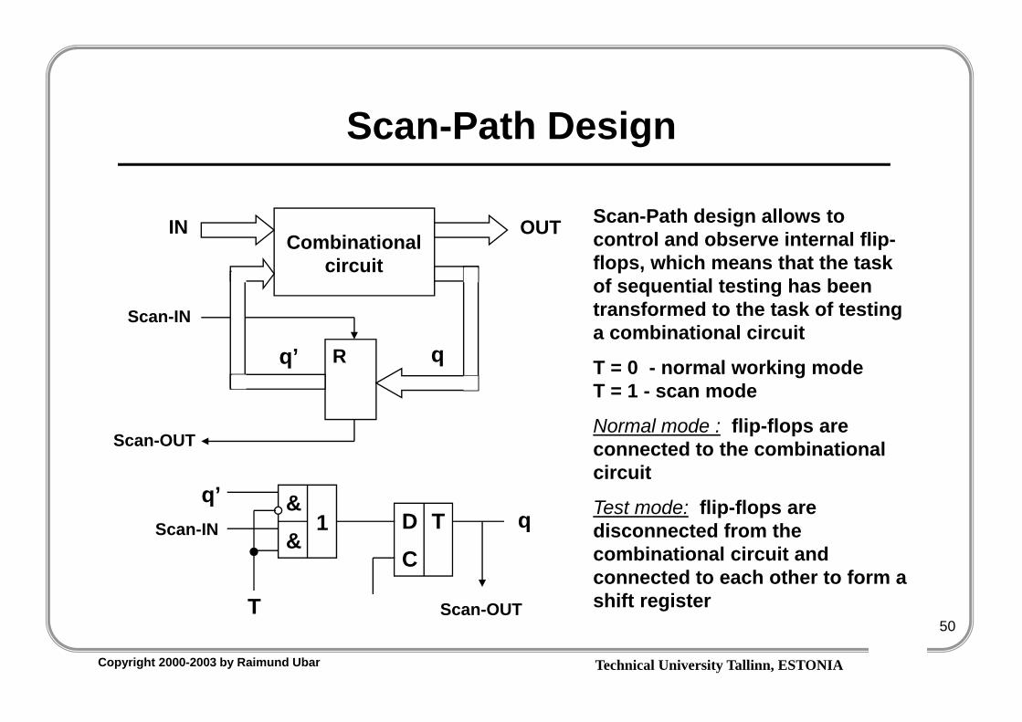
Scan-Path Design
Combinational circuit
IN OUT
R
Scan-IN
Scan-OUT
1&&
q
q’Scan-IN
T
TDC
Scan-OUT
q
q’
Scan-Path design allows to control and observe internal flip-flops, which means that the task of sequential testing has been transformed to the task of testing a combinational circuit
T = 0 - normal working mode T = 1 - scan mode
Normal mode : flip-flops are connected to the combinational circuit
Test mode: flip-flops are disconnected from the combinational circuit and connected to each other to form a shift register

Technical University Tallinn, ESTONIACopyright 2000-2003 by Raimund Ubar
51
Scan-Path Design and Testability
OUTMUX
DMUXIN
SCANOUT
SCANIN
Two possibilities for improving controllability/observability

Technical University Tallinn, ESTONIACopyright 2000-2003 by Raimund Ubar
52
Parallel Scan-Path
Combinational circuit
IN OUT
R1
Scan-IN 1
Scan-OUT 1
R2
Scan-IN 2
Scan-OUT 2
In parallel scan path flip-flops can be organized in more than one scan chain

Technical University Tallinn, ESTONIACopyright 2000-2003 by Raimund Ubar
53
Partial Scan Path
M3
e+M1
a
*M2
b
R1
IN
c
d
y1 y2 y3 y4
y4
y3 y1 R1 + R2
IN + R2
R1 * R2
IN* R2
y2
R2 0
1
2 0
1
0
1
0
1
0
R2
IN
R12
3
Hierarhical test generation with Scan-Path:
Control Part
R2Bus
Scan-In
Scan-Out
Data Part

Technical University Tallinn, ESTONIACopyright 2000-2003 by Raimund Ubar
54
Logical BIST
• Test Microprogram
• Parameters– Program
steps – Used reisters– Tested
functions

Technical University Tallinn, ESTONIACopyright 2000-2003 by Raimund Ubar
55
Random Access Scan
Combinational circuit
IN OUT
R qq’
&Scan-INScan-CL
Scan-OUT
DC
DC
X-Address
Y-Address
In random access scan each flip-flop in a logic network is selected individually by an address for control and observation of its state
Technical University Tallinn, ESTONIACopyright 2000-2003 by Raimund Ubar
56
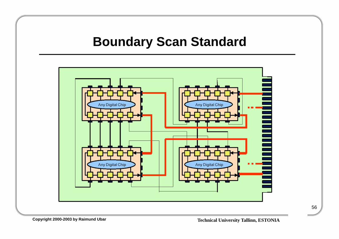
Boundary Scan Standard
Technical University Tallinn, ESTONIACopyright 2000-2003 by Raimund Ubar
57
Conclusions
• Self-Test of modules (components) is important, but is not the Panacea
• Hierarchical and Functional Test have the same importance
• Functional Fault Model is a universal means for mapping defects, faults and errors from level to level, providing a formal basis for hierarchical approach
• Decision Diagrams can be used successfully not only at logical levels, but also at higher RTL or behavioral levels

Technical University Tallinn, ESTONIACopyright 2000-2003 by Raimund Ubar
58
References
• Contact data: – Tallinn Technical University– Computer Engineering Department– Address: Raja tee 15, 12618 Tallinn, Estonia– Tel.: +372 620 2252, Fax: +372 620 2253– E-mail: [email protected]– www.ttu.ee/ˇraiub/
Technical University Tallinn, ESTONIACopyright 2000-2003 by Raimund Ubar
59
Overview
1. Introduction2. Theory: Boolean differential algebra3. Theory: Decision diagrams4. Fault modelling5. Test generation6. Fault simulation7. Fault diagnosis
8. Testability measuring9. Design for testability10. Built in Self-Test
Technical University Tallinn, ESTONIACopyright 2000-2003 by Raimund Ubar
60
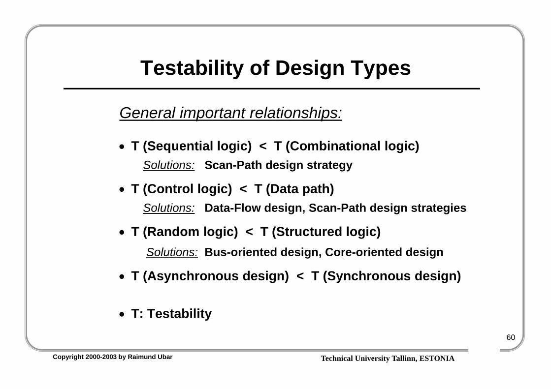
Testability of Design Types
General important relationships:
T (Sequential logic) < T (Combinational logic)Solutions: Scan-Path design strategy
T (Control logic) < T (Data path)Solutions: Data-Flow design, Scan-Path design strategies
T (Random logic) < T (Structured logic)Solutions: Bus-oriented design, Core-oriented design
T (Asynchronous design) < T (Synchronous design)
T: Testability

Technical University Tallinn, ESTONIACopyright 2000-2003 by Raimund Ubar
61
Testability Estimations for Circuit Types
Circuits less controllable
• Decoders• Circuits with feedback• Counters• Clock generators• Oscillators• Self-timing circuits• Self-resetting circuits
Circuits less observable
• Circuits with feedback• Embedded
– RAMs– ROMs– PLAs
• Error-checking circuits• Circuits with redundant
nodes
Technical University Tallinn, ESTONIACopyright 2000-2003 by Raimund Ubar
62
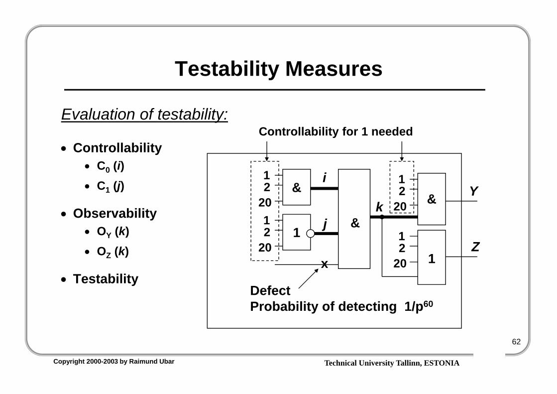
Testability Measures
Evaluation of testability:
Controllability C0 (i) C1 (j)
Observability OY (k) OZ (k)
Testability
12
20&
&12
201
x
DefectProbability of detecting 1/p60
12
20 &
12
20 1
i
kj
Y
Z
Controllability for 1 needed
Technical University Tallinn, ESTONIACopyright 2000-2003 by Raimund Ubar
63
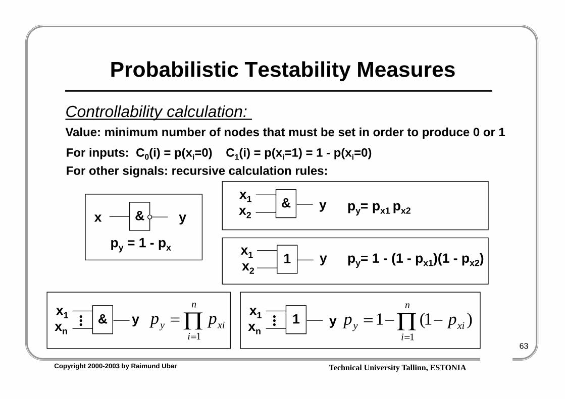
Probabilistic Testability Measures
Controllability calculation: Value: minimum number of nodes that must be set in order to produce 0 or 1For inputs: C0(i) = p(xi=0) C1(i) = p(xi=1) = 1 - p(xi=0) For other signals: recursive calculation rules:
&x y&x1 yx2
1x1 yx2
py= px1 px2
py = 1 - pxpy= 1 - (1 - px1)(1 - px2)
&x1 yxn
... xi
n
iy pp
1
1x1 yxn
... )1(11
xi
n
iy pp
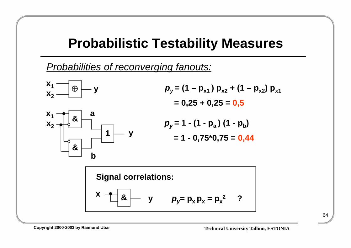
Technical University Tallinn, ESTONIACopyright 2000-2003 by Raimund Ubar
64
Probabilistic Testability MeasuresProbabilities of reconverging fanouts:
x1 yx2
&x1
yx2
&1
py = 1 - (1 - pa ) (1 - pb)
= 1 - 0,75*0,75 = 0,44
a
b
&x y py= px px = px2 ?
Signal correlations:
py = (1 – px1 ) px2 + (1 – px2) px1
= 0,25 + 0,25 = 0,5
Technical University Tallinn, ESTONIACopyright 2000-2003 by Raimund Ubar
65
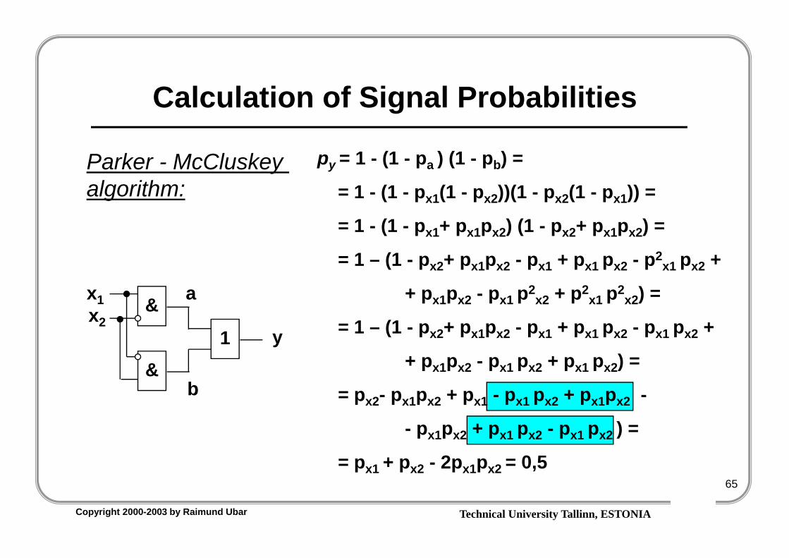
Calculation of Signal Probabilities
&x1
yx2
&1
py = 1 - (1 - pa ) (1 - pb) =
= 1 - (1 - px1(1 - px2))(1 - px2(1 - px1)) =
= 1 - (1 - px1+ px1px2) (1 - px2+ px1px2) =
= 1 – (1 - px2+ px1px2 - px1 + px1 px2 - p2x1 px2 +
+ px1px2 - px1 p2x2 + p2
x1 p2x2) =
= 1 – (1 - px2+ px1px2 - px1 + px1 px2 - px1 px2 +
+ px1px2 - px1 px2 + px1 px2) =
= px2- px1px2 + px1 - px1 px2 + px1px2 -
- px1px2 + px1 px2 - px1 px2 ) =
= px1 + px2 - 2px1px2 = 0,5
a
b
Parker - McCluskey algorithm:

Technical University Tallinn, ESTONIACopyright 2000-2003 by Raimund Ubar
66
Calculation of Signal Probabilities
Straightforward methods:
&
&
&
a
c
y&
b
1
2
3
21
22
23
Parker - McCluskey algorithm:
py = pcp2 = (1- papb) p2 =
= (1 – (1- p1p2) (1- p2p3)) p2 =
= p1p2 2 + p2
2p3 - p1p23p3 =
= p1p2 + p2 p3 - p1p2p3 = 0,38
Calculation gate by gate:
pa = 1 – p1p2 = 0,75,
pb = 0,75, pc = 0,4375, py = 0,22
For all inputs: pk = 1/2