ieee transactions on very large scale ...users.ece.gatech.edu/phasler/published_papers/fpaa...sihwan...
TRANSCRIPT

This article has been accepted for inclusion in a future issue of this journal. Content is final as presented, with the exception of pagination.
IEEE TRANSACTIONS ON VERY LARGE SCALE INTEGRATION (VLSI) SYSTEMS 1
Integrated Floating-Gate ProgrammingEnvironment for System-Level ICs
Sihwan Kim, Jennifer Hasler, Senior Member, IEEE, and Suma George
Abstract— We present the first integrated system to handleheterogeneously used and programmed floating-gate (FG)elements in a single modular approach. We focus on IC design,integration, characterization, and algorithmic developmentof an integrated FG programming system for a large-scale field-programmable analog array. We work throughtunneling approaches to initialize the FG devices for precisionprogramming, as well as hot-electron injection approaches forprecise device programming.
Index Terms— Floating-Gate Programming.
I. INTRODUCTION
WE PRESENT the first IC system to program hetero-geneous digital and analog floating-gate (FG) ele-
ments in a single modular approach. This paper focuseson the IC design, integration, characterization, and algo-rithms of an integrated FG programming system for system-level ICs, such as large-scale field-programmable analogarrays (FPAAs) [1], [2].
Fig. 1 shows the high-level view of the current FG program-ming approach implemented in this IC system. This program-ming system only requires that the IC user simply downloadthe desired programming file, including code and FG devicesto program into the IC. The on-chip components, such asDACs, ADCs, and microprocessor (μP), for programming aredrop-in modules for a larger programmable system design.
This paper’s approach builds an FG programming algorithmrequiring only a few fixed-point computations. This paperrequires a fresh look into FG programming techniques andalgorithms, particularly, when the FG programming approachmust work for highly diverse circuit functions. Precisionprogramming of FG devices uses hot-electron injection due tothe nearly ideal selectivity between the devices, while globalinitialization uses electron tunneling due to the relativelypoor device selectivity [3], [4]. Target programming usinghot-electron injection requires measuring the channel current(14-bit fixed-point value) and computing the voltages(7-bit fixed-point DAC value) for the next injection pulse.
These approaches are based on the previous component-level hardware structure [5], hot-electron injection [6], [7],and discussions on programming very low target currents [8].The previous MATLAB-based algorithms required extensivefloating-point computations. Specialized FG circuit program-ming, such as voltage sources [9]–[16], or standard digital
Manuscript received April 6, 2015; revised July 21, 2015 andOctober 2, 2015; accepted November 5, 2015.
The authors are with the School of Electrical and Computer Engineer-ing, Georgia Institute of Technology, Atlanta, GA 30332-250 USA (e-mail:[email protected]).
Digital Object Identifier 10.1109/TVLSI.2015.2504118
Fig. 1. FG programming approach we describe in this paper, enabling a directdownload, as typical of digital programming (i.e., SRAM chains for FPGAs)has programmed switch and parameter information. This process empowersthrough complete on-chip FG analog and digital targeted programming to aheterogeneous set of FG circuits and computing devices. The programmingstructure uses on-chip DACs, ADCs, and a 16-bit open-source processoravailable for postprogramming computation. From the user’s perspective, aftertheir design has been compiled, like on a large-scale FPAA, the resultingprogramming operation looks like a typical data-download operation to anembedded device.
memories [17]–[22] are both far too constraining for a hetero-geneous array of computations; nondigital memory approachesfall short of user-friendly interfaces (e.g., downloading adevice switch list). This paper experimentally shows the mea-sured results unless otherwise mentioned.
II. FG PROGRAMMING INFRASTRUCTURE
We first discuss the infrastructure and programmingframework before jumping into the physics and program-ming discussions. Fig. 2 shows our standard for accessingthe FG devices for programming. We show a representativestructure, including switches and active devices, typical of acomputational analog block in a large-scale FPAA device [25].For programming, the entire circuitry gets reconfigured intoa single crossbar array. We program in a crossbar arraybecause hot-electron injection is a product of the current inthe transistor channel and the voltage between the drain andchannel potentials (≈near source voltage); by only allowingcurrent for a particular column and by only allowing a
1063-8210 © 2015 IEEE. Personal use is permitted, but republication/redistribution requires IEEE permission.See http://www.ieee.org/publications_standards/publications/rights/index.html for more information.

This article has been accepted for inclusion in a future issue of this journal. Content is final as presented, with the exception of pagination.
2 IEEE TRANSACTIONS ON VERY LARGE SCALE INTEGRATION (VLSI) SYSTEMS
Fig. 2. When using a heterogeneous array of FG devices, we require that all FG devices are reconfigured into a single crossbar array of FG devices. In thisconfiguration, we can program using hot-electron injection with nearly perfect selectivity, because a device requires channel current and high voltage fromthe drain-to-channel potential. Sometimes, we have additional control structures to guarantee transistor currents are turned OFF when not selecting a column;for example, a switch programmed ON will have some current in the case when its Vg is at Vdd . Reconfigurability between the program mode and the runmode is essential to enabling programming of all potential FG elements. The significance of this crossbar array and the gate and drain selecting multiplexersis that we can talk about addressing, measuring, and programming a single device in the array; equivalent to a device separated from the rest of the array.
high voltage between the drain and source terminals on aparticular row, we are assured that only the desired deviceis affected. As a result of the nearly ideal selectivity dueto the AND process for hot-electron injection and resultingselectivity for each transistor’s current–voltage response,this entire structure effectively collapses as a singleFG pFET device with a selected gate and drain terminal.We globally erase and restore devices by electron tunnelingeffects, partially because of the limited selectivity of thesetwo-terminal devices typical of most physical two-terminaldevices. When we program a device, we can measure thedevice properties in as close a situation as desired to the actualoperation, therefore minimizing the effect of parasitic elementsdegrading the resulting programming accuracy when we movefrom the program mode to the run mode.
Fig. 3 shows the board and on-chip infrastructure. Fig. 3(a)shows the board-level infrastructure for programming andaccessing the FG programming structure, as well as thedigital infrastructure for accessing the chip during the normalprogramming operation. Fig. 3(b) shows the high-levelblock diagram for the on-chip programming structure,which includes utilizing an open-source μP, embedded16 k × 16 SRAM for program and data memory, as well asthe memory-mapped registers which control the elements forprogramming. We see in Fig. 2 that we simply need to controlthe gate and drain voltage (through two separate DACs) andthen measure the resulting device current, which is at the coreof the structure. The accuracy of the gate and drain DACs isnot directly correlated with the final programmed accuracy; thefrequency and noise of the ADC, which is 14 bit, are directlyrelated to the final programming accuracy.
III. ON-CHIP INTEGRATED FG PROGRAMMING
Our FG programming relies on a combination of electrontunneling for erasing and resetting FG devices and hot-electroninjection for programming FG devices. Fig. 4 shows theFG programming framework, with the resulting tunneling andinjection steps. Over Sections III-A–III-D, we will discussthe global erasing and initialization (reverse tunneling) steps,FG recovery by injection, FG rough programming throughopen-loop injection, and final short step of FG fine program-ming through predictive FG calculations.
A. Global Array Erasure and Initialization
Erasing a block requires raising an entire block of tunnelingjunction voltages (Vtun) to a sufficiently high voltage to movetoward a high FG voltage, which in turn results in a lowchannel current (i.e., fA in a pFET device) while still allow-ing programming to the desired target location. We initiallytunnel all the FG values to a high voltage that ensures apFET device has no channel current, and then we performa reverse-tunneling operation to bring FG voltages to a small,but negligible, pFET current for a gate selection voltage at 0 V.Electron tunneling for erasing blocks is a common approachfor erasing FG devices [3]–[7]. The 12 V charge-pump IC isonly operational during the tunneling erase operation. Onecould choose to tunnel the voltage just enough to reach asufficiently low current and measure a few representativecurrents, expecting that all the devices are erased. Unfortu-nately, tunneling current measurements for identical operatingconditions show a variability of 2–3 (or more), resulting inexponentially different rates between the devices. Therefore,

This article has been accepted for inclusion in a future issue of this journal. Content is final as presented, with the exception of pagination.
KIM et al.: INTEGRATED FG PROGRAMMING ENVIRONMENT FOR SYSTEM-LEVEL ICs 3
Fig. 3. Integrated infrastructure blocks, including test board, high-levelIC schematic for programming, and detailed programming schematic. (a) Sys-tem interface block diagram used for programming a representative FPAAdevice with the on-chip open-source MSP430 μP and memory. The pri-mary off-chip infrastructure is μP IC-controlled high-voltage power handling(12 and 6 V charge-pump ICs); these components were left off-chip tominimize the IC design risk. A USB to serial converter IC was chosen tointerface to μP. (b) Core on-chip circuit infrastructure used for μP-basedprogramming arrays of FG devices. The μP and integrated 16 k × 16 SRAMblock programming FG devices through a sequence of memory-mappedregisters for the DACs supplying the gate and drain voltages, the FG currentmeasurement structure using a ramp ADC, and two pFET transistors toconvert from the current to the voltage. We estimate the processor requiresapproximately 200 pJ per instruction, including the local memory access.
without measuring all the devices, we tunnel enough so thateach device’s FG voltage is sufficiently high.
Reverse tunneling turns the polarities around on thetunneling junction to bring the resulting currents back towarda small but reasonable current for injection with less devicemismatch than tunneling. The reverse tunneling phase requireslower voltages; for the 350-nm IC process, voltages between0 and 6 V are used, resulting in lower charge across thetunnel oxides. The resulting code for implementing thesetwo phases only requires applying the desired voltages, waitinga particular timeframe (allowing the processor to shut down ordownload programming instructions), and resetting voltages tothe normal operating condition.
B. First Injection Step: FG Recovery
Once we have cleared all of the FG devices (FG voltagesufficiently high), we begin the process of programmingFG devices that have nonnegligible current. FG pFET devicesthat we do not program will stay in accumulation and pullnegligible levels (<1 pA) of current, even for scaled-downdevices. Furthermore, our FG devices in the run mode are
biased with Vg at roughly 0.6 V, enabling the algorithm toobserve lower current values by measuring current at Vg at 0 V.For the IC used for measurements, we had a constant leakagecurrent, due to the reverse-bias source–drain junction currentsnear 1 nA, thereby enabling current measurements in the10–30-pA range even with this high leakage current. For aswitch FG device, we typically measure 30 pA of currentfor Vg at 0.6 V but 1 nA for Vg at 0 V; for deviceswith larger FG capacitive coupling, this effect is evenstronger.
The initial process simply looks for a significant channelcurrent (i.e., 20–30 nA) when measuring current at Vg = 0 Vfor a switch element corresponding to 1 nA for Vg = 0.6 V;levels for a significant channel current differ for differentgroups of FG devices with different capacitive couplings.Furthermore, we have a programming sequence in parallelto what is shown in Fig. 4 for lower currents (<1 nA forswitches) where we just simply inject until we have roughly1 nA of current for Vg = 0 V, enabling targeted currentsbetween 30 pA and 1 nA as needed. One can modify thedrain voltage for the pulses to move the current values closer.
C. Approximate FG Programming by Injection
Target programming typically requires measuring channelcurrent, comparing it with the desired current, performing arange of calculations for the conditions (i.e., drain voltage)during the next injection pulse, and repeating until it suffi-ciently converged. Previously, these calculations were rathercomplex, particularly, for a fixed-point embedded process-ing environment, giving an opportunity to reformulate thisapproach to fit better with fixed-point arithmetic.
We start by describing our measurement of the channel cur-rent at a compressed FG voltage through the 14-bit ramp ADC,as shown in Fig. 5. We are measuring an FG pFET devicethrough the drain current switched through the programmingcrossbar infrastructure. Measuring current typically requiresa conversion from current to voltage, and we potentiallyrequire four-to-seven orders of magnitude in our measurement.Therefore, we need some form of compression; in this case,a better approach would be translating the current into arepresentation near the original voltage difference from thewell voltage to the FG voltage. We use a pFET device withthe drain voltage tied to the gate voltage with the specialcase of the well voltage tied to the source voltage for ourmeasurement circuitry. Fig. 5 also shows the reduced circuitto look at the resulting relationship between the FG voltageand the resulting Vout. A straightforward, large signal analysisof this circuit (assuming matched devices) shows
Vout = 2(Vdd − Vfg). (1)
Threshold voltage variations simply require adding terms tothe resulting structure.
We look next at the resulting-type S curves, taken froman FG switch element, looking at this Vout, which is directlyrelated to Vfg. For a starting (subthreshold) drain current,injection decreases the FG voltage, increasing the draincurrent, further decreasing the FG voltage. The process slowsdown as the current moves to above-threshold operation

This article has been accepted for inclusion in a future issue of this journal. Content is final as presented, with the exception of pagination.
4 IEEE TRANSACTIONS ON VERY LARGE SCALE INTEGRATION (VLSI) SYSTEMS
Fig. 4. Algorithm steps for programming an array of FG devices. Top: block diagram of the key required programming steps. The overall programmingsequence requires putting the programming code into memory (for each operation), erasing and recovering devices through electron tunneling, reverse tunneling,and an additional recovery injection step, injecting FG switches where used, and then using a sequence of course and fine injection phases to reach the targetfor the subthreshold and above-threshold currents. In each case, switch data are loaded into the data SRAM block, programmed, and then additional pagesof data are input to finish a phase if necessary. The final steps are loading the SRAM memory for the code desired (if necessary) for the IC operation andthen switching the IC into the run mode. Left: graphical illustration of the FG programming steps following the procedure for a range of FG devices startingand ending at a desired target value. Right: experimental data showing actual trajectories of four FG devices through the first four programming steps; Fig. 5will show the remaining precision injection measurements. The goal is to get devices close to target programming. Our devices operate in the run mode,biasing Vg at roughly 0.6 V; our measurements start with Vg at 0 V to measure devices with low currents and enable FG precision targeting for currentsbelow the ≈1-nA measured leakage current from the array.
(defined as significantly greater than the threshold currentor Ith), because as the FG voltage decreases, the increaseddrain current decreases the drain-to-channel voltage availablefor injection due to the additional voltage drop across thechannel. This response, designated S curve, given the shapeof the response.
Fig. 5 shows a measurement of Vout after an injection pulse(always for Vd to 0 V for a 6 V Vds) versus the initialmeasured Vout; this process was repeated until reaching anear steady-state solution. For these measurements, we used apulsewidth of 10 μs. We measure the output through the ADC,which follows the linear relationship:
Vout[n] = 0.0001602a[n] + 0.3490 (2)
where a[n] is the 14-bit integer code (0 through 16 383)measured in the ADC (we can keep all the codes withinthe 14-bit code on the 16-bit processor). Fig. 5 also showstwo straight-line curve fits to the resulting data, as well as the
table for the equation both in Vout and a, allowing simple,fixed-point computations for targeted programming.
Typically, we use a single pulse time width Tinj for everypulse, although the timing could be modified where desired.Therefore, the better the computational model, the fewer thenumber of pulses, and the shorter the resulting programmingtime (assuming the computation is fast). The fundamentalmodel for hot-electron injection current (Iinj), using transistorsoperating with the subthreshold or near subthreshold biascurrents [23], [24]
Iinj = Ise f (Vfg,�dc) ≈ Iinj0
(Is
Iso
)α
e�dc/Vinj (3)
where Vinj represents the one parameter for the f (·, ·)linearization. with all voltages relative to its Vdd . At each step,we should be exponentially decreasing the percentage changeneeded for the target, improving 1 bit of accuracy per iteration.Many combinations of Vg and Vd schemes are possible for thealgorithm. The S curves have exponential growth in FG voltage

This article has been accepted for inclusion in a future issue of this journal. Content is final as presented, with the exception of pagination.
KIM et al.: INTEGRATED FG PROGRAMMING ENVIRONMENT FOR SYSTEM-LEVEL ICs 5
Fig. 5. Movement from the basic FG circuit array elements to course programming algorithm. Path from FG to Vout: crossbar network of indirect FG devicescommunicates through the drain current outputing a voltage through two pFET devices directly related to the FG voltage. Each FG device must be measuredas well as enabled for hot-electron injection. Circuit analysis: equivalent circuit from the FG voltage (Vfg) to the output voltage (Vout). Using the same size(or similar size) pFET devices (Vsw = 0) implies that transistor k match, resulting in �Vout / �V f g = 2. Measured data from Vout[n] (start) to Vout[n + 1](final): measurement of the final value after injection for Vout on the current measurement versus the initial value before injection for Vout on the currentmeasurement for maximum injection drain voltage pulse (6 V). Two straight-line curves, modeling the subthreshold part of the regime and the above-thresholdpart of the regime, enable the fixed-point computation for the updates for the on-chip μP with a simple fixed-point multiply and addition operations. Voutto course programming: using this data, the first initial injection jumps require simple operations (that can be stored in a table) due to the linear modeling,making an open-loop jump for a particular number of pulses or pulsewidth, based on the target value, as well as for iterative jumps based on Vout measurementto get the FG voltage within a single pulse spacing. Lower equations: resulting extracted (and used) Vout equations expressed both in the measured voltage,as well as in the measured 14-bit ADC codeword (a[n]).
(exponentially growing from an unstable equilibrium) for thesubthreshold and near-threshold measurements and exponen-tial convergence (exponentially decreasing toward a stableequilibrium) for higher above-threshold measurements.
From this framework, the next stages for the programmingalgorithm include a first injection phase, then a measuredinjection phase to get results within one pulse step, readyfor the last sequences of fine programming. Fig. 4 shows theresults of four representative trajectories where target levelsare 0.5, 1, 5, and 10 μA. Since the starting drain current andmeasured Vout are roughly the same (≈1–2 nA), and we havegood matching between these parameters on an IC, we usea first injection pulse to approximate but not overshoot thetarget level. From the extracted linear curve, we can make atable (shown in Fig. 5) of the target value as a function of thenumber of pulses on a given device. A longer pulsewidth isroughly equivalent to multiple pulses of the same total time.
The table is not large, since in 29 steps, we reach thecross over point, and in 48 pulses, we are at the top of thesecond curve, resulting in under 500 μs for this open-loopprogramming step; a full 14-bit measurement, using a typical25-MHz clock, takes roughly 1 ms to complete, so theseinjection measurements, even at 6 V, are shorter than a fullmeasurement. These approaches are not limited by the speedof the μP. This first step does not require an additionalmeasurement, reducing the programming time.
Next, μP calculates the number of pulses, based on mea-surement, to reach within one pulse of the target withoutovershooting the device. Effectively, if we had zero mismatchin the array, this step would be unnecessary, but we use thisstep to get devices within one injection step even with potentialdevice mismatches. We will repeat this step as needed.
D. Precise Targeted FG Injection Programming
Our programming approach starts by measuring the desireddevice current, comparing that result with the desired targetresult, and computing the desired drain and/or gate voltagesused to reach the desired target without overshooting thedesired result. After the system applies the programming pulse,it proceeds to measure the new device current and repeats untilsufficient accuracy has been achieved.
Targeted programming in one sense is the one aspectin this paper that leans heavily on the previous history ofFG programming algorithms, including targeted subthresholdand near-threshold devices [7], adaptive targeting of sub-threshold currents [6], and early efforts using on-chip ADCfor current measurement [5]. In another sense, our approachfor this phase of programming takes a different turn byconstraining/considering FG targeted programming using thefixed-point, reduced arithmetic using lower precision DACsthan the precision of the targeted value while still obtainingthe required high accuracy on a single FG device.
This article has been accepted for inclusion in a future issue of this journal. Content is final as presented, with the exception of pagination.
6 IEEE TRANSACTIONS ON VERY LARGE SCALE INTEGRATION (VLSI) SYSTEMS
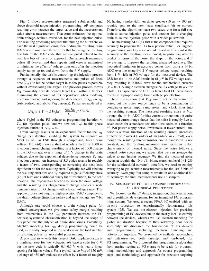
Fig. 6 shows representative measured subthreshold andabove-threshold target injection programming. μP computesresulting error between the target value and the measurementvalue after a measurement. That error estimates the optimaldrain voltage, without overshoot, for the next injection pulse.The resulting processing requires first finding the bit where wehave the next significant error, then finding the resulting drainDAC code to minimize the error for that bit, using the resultingfew bits of the DAC code that are computed related to thenext few bits of the error approach. Our approach measures,pulses all devices, and then repeats until error is minimizedto minimize the effect of voltage transients after the injectionsupply ramps up to, and down from, the 6 V supply.
Fundamentally, the task is controlling the injection processthrough a sequence of measurements and pulses of fixedtime (Tinj), to hit the desired target in as few pulses as possiblewithout overshooting the target. The previous process movesVfg reasonably near its desired target (i.e., within 100 mV),minimizing the amount of FG dependence when modelinginjection current, and ignoring the dependence of Iinj on Vfg(subthreshold and above VT 0 currents). Pulses are modeled as
�Vfg[n + 1] ≈ �Vfg[n] − Iinj0Tinj
CTe−�Vd/Vinj (4)
where Vfg[n] is the FG voltage at programming iteration n,Tinj for injection pulse, and we now set Iin j0 to this phaseinjection current at �Vd = 0.
Drain voltage results in an exponential factor for the Vfgchange per iteration, enabling the system to improve onMSB as well as LSB through a compressed, linear drainvoltage. Fig. 6(d) shows a shift of nearly a factor of 1000 ininjection current change, resulting in a factor of 1000 changein the FG voltage, over a range of 1 V change in the drainvoltage, due to the exponential dependence between Vd andinjection current. An increase of 3.5 codes results in roughlya factor of two, corresponding to correcting the next leastsignificant bit for the resulting error. Typically, we will tabulatethe resulting error size and Vd required to get sufficiently close(i.e., at least one additional binary bit of resolution) to the nextiteration. The exponential function between the drain voltageand the resulting FG charge/current change enables a widedynamic range of FG changes with a linear voltage range. Thisapproach does not require high-precision DAC components;the drain voltage (injection pulse) and gate voltage are 7-bitDACs.
Although one could choose a drain voltage pulse foroptimal convergence, we give some safety margin resultingfrom mismatches in the Vinj parameter between the FGdevices; systematic characterization is beyond the scope ofthis paper but the subject of future discussions. Potentially,adaptive modeling for Vinj during programming could beused, as initially proposed in [6], to decrease the total numberof resulting pulses for successful programming.
A practical issue with this current DAC implementation isa nonlinear step for low voltages. We have a code for 0 V,but the next code is typically 0.4–0.5 V with nearly linearspacing for higher values. For a typical value Vinj of 150 mV,a change of 450 mV reduces the effect by a factor of roughly
20; having a pulsewidth ten times greater (10 μs → 100 μs)roughly gets to the next least significant bit to correct.Therefore, the algorithms have two cases, one for a full sizedrain-to-source injection pulse and another for a changingdrain-to-source injection pulse with a wider pulsewidth.
The measuring ADC (14 bit) is the component that requiresaccuracy to program the FG to a precise value. For targetedprogramming, one key issue not addressed at this point is theaccuracy of the resulting measurement, in particular, what topredict in terms of the noise, the shape of the noise, and ifwe average to improve the resulting measured accuracy. Thetheoretical limitation in accuracy comes from using a 14-bitADC over the (roughly) 2 V output voltage range, resultingfrom 1 V shift in FG voltage for the measured device. TheLSB for the 14-bit ADC results in 61 μV in FG voltage accu-racy, resulting in 0.166% error for the subthreshold currents(κ = 0.7). A single electron changes the FG voltage 10 μV fora total FG capacitance of 16 fF; a larger total FG capacitanceresults in a proportionally lower voltage per electron.
These results show that Vout would not be the source ofnoise, but the noise source tends to be a combination ofcomparator noise, input ramp noise, and clock jitter intothe resulting counter. The measured resulting noise at Voutthrough the 14-bit ADC for bias currents throughout the entiremeasured current range shows that the noise is roughly five toseven codes for a standard deviation (two codes as a functionof USB power supply noise, lower noise at lower current), thenoise is a weak function of the resulting current (increasesa factor of 2 over 4+ orders of magnitude in current), eventhough the resulting three-transistor circuit bandwidth is notconstant, and the resulting measured noise spectrum is flat,characteristic of thermal noise. Since the noise follows athermal noise spectrum, we expect that we can average thevalues to get further accuracy. We find the measured noiseoccurs at roughly the 10-bit/11-bit measurement level (<1–2%for the subthreshold currents); therefore, we need to employaveraging to get accurate measurements for the last 3 bits ofaccuracy. Averaging four samples results in one additional bitof accuracy; the final measurements use 16 samples.
IV. SUMMARY OF FG PROGRAMMING: PERFORMANCE
AND HISTORICAL PERSPECTIVE
We focused on the IC design, integration, characterization,and algorithmic development for an integrated FG program-ming system. We used a recent FPAA IC enabled with anon-chip processor to experimentally demonstrate thissystem [25]. We use hot-electron injection for precisionprogramming of FG devices due to the nearly ideal selectivitybetween the devices, whereas we use electron tunneling forglobal initialization because of their relatively poor deviceselectivity. We discussed the foundations of FG devicesand programming, including electron tunneling andhot-electron injection. We presented the methods, approaches,and infrastructure, both on-chip and on-board, forFG programming. We discussed this programming algorithmfrom erasing, setting up FG charge to be ready for program-ming, methodology and approach for course programmingsteps, and methodology and approach for precision targeting

This article has been accepted for inclusion in a future issue of this journal. Content is final as presented, with the exception of pagination.
KIM et al.: INTEGRATED FG PROGRAMMING ENVIRONMENT FOR SYSTEM-LEVEL ICs 7
Fig. 6. Precision programming measurements for the subthreshold and above-threshold currents, showing representative course injection, measured courseinjection (single Vd ), and precision target injection. (a) Four target current measurements for the subthreshold currents. (b) Four representative currentmeasurements for the above-threshold currents. We programmed several different FG devices to these currents and summarize the average measurement erroras well as the standard deviation over the average current from these multiple measurements using this entire programming infrastructure. Since injectioncurrent and the change in FG voltage are an exponential function of drain (Vd ) voltage, the resulting drain pulse is approximated by pulling apart the differenceof target and measured values. (c) Percentage accuracy for target programming for a range of currents, including the standard deviation after performingmultiple injection target programming rounds. (d) Values for relevant drain DAC codes, and their change on the injection current through a change in Vdduring the programming injection pulse. A constant Vinj of 150 mV (typical value) is assumed for these calculations; in practice, there is some weak curvatureto these calculations over this range of evaluation. A change of 4 (2 bits) occurs for the transition through seven codes or 210 mV.
steps, all based on the opportunities afforded to us throughthe current infrastructure.
Table I summarizes the memory requirements, pulse, andcomputation time for programming steps, and resulting energyestimate required for performing these steps. Table II shows atypical switch list for the coordinates of the FG devices to beprogrammed, their resulting current to be programmed (whererelevant) or switch type, as well as the type of FG device(i.e., particular CT ) used. We programmed many FG devicesin a large array (over 200 000 devices) using these definitionsthat can be compiled from higher level tools. Fig. 7 showsthe die photographs of the key components for programming,including the programmer module (DACs, ADCs, and so on),the open-source MSP430 μP, and the resulting 16 k × 16SRAM block used for the data and memory. The biggest issue
Fig. 7. Die photo of the programmer infrastructure, μP, and SRAM memory(16 k × 16) in a 350-nm CMOS process. The area of the SRAM memory ismuch larger than the other two blocks.
in terms of size and power dissipation during programming isdue to SRAM size and communication.
The time estimates do not include the required measurementtime, roughly 7-ms per measurement requiring 0.5 s toprogram a single targeted device, which in the current

This article has been accepted for inclusion in a future issue of this journal. Content is final as presented, with the exception of pagination.
8 IEEE TRANSACTIONS ON VERY LARGE SCALE INTEGRATION (VLSI) SYSTEMS
Fig. 8. Pictorial history of FG circuit programming algorithms developed at Georgia Tech, where we show the complexity for on-chip computation, aswell as board and overall infrastructure required for a programming step. FG devices started from the original single transistor synapse learning device [4],and developed into a range of FG circuit applications (one summary in [3]). The approaches start with external bench-top instruments programming a fewFG devices [3], to an interface PC board with simple interface to allow computer control [6], to a PC board + field-programmable gate array (FPGA) boardsolution to perform the programming infrastructure along with MATLAB programming control [7], to having some of the circuit infrastructure on board as aprogrammer module [5], with an on-board microcontroller with MATLAB control of the programming algorithm, and to final our current integrated solutionwith the entire programming control and infrastructure entirely on the IC requiring no μP control over the process other than writing the proper file formatto the IC. At each level, we roughly increased the number of FGs routinely programmed by an order of magnitude, going from 10 to 100, to 1 k to 10 k toour current structure routinely programming arrays of 100 k or larger, such as our current family of FPAA devices, further enabling larger and larger systemapplication solutions. Our approach also enables using both direct and indirect programming, whether we have nFET or pFET devices.
TABLE I
TABLE OF PARAMETERS FOR μP MEMORY SIZE, TYPICAL COMPUTATION
TIME, AND RESULTING ENERGY ESTIMATE FORTHAT FULL OPERATION
implementation consumes most of the resulting programmingtime. Practically, this limitation means we use injectionsupply at 6 V. The Vout measurement requires less than 1 msfor currents less than 1 nA; therefore, this component is not alimitation, and the measurement can be further accelerated asneeded. The resulting issue is measurement through a single14-bit ramp ADC used in our IC required to measure thefull resolution using a 10-MHz down sampled clock (from20–25-MHz processor clock). We see an opportunity inbuilding more intelligence into the ADC measurement basedon variations on the ramp function. For example, we canuse the ADC as a threshold when we need a course targetvoltage. As another example, we can see setting the rampbetween the 6- and 8-bit linear DAC values to enable fasterprecision measurement, increasing the ramp measurement bya factor of 64 or further. We see these issues as being thenext level question for programming large-scale FG arrays.Furthermore, as devices scale to millions of devices, we can
TABLE II
PART OF TYPICAL SWITCH LIST
visualize using parallel measure and program components,organized for blocks of FG devices used to minimize theprogramming time. The ramp ADC structure could easilybecome a parallel bank of ADCs, and the small amount ofμP assembly code could allow for multiple device operation.
The programming approach shown in Fig. 2 focused onenabling arrays of arbitrary FG devices, creating the mini-mal number of rules/constraints for this implementation, andthereby separating the design of FG circuits and systemsfrom the FG programming issues. Large FG systems requireautomatic programming of arbitrary circuits, particularly forsystems with high configurability that have to be enabledby higher level tools. These approaches required going pastthe basic FG transistor concepts, operation, and program-ming physics, including requiring hot-electron injection forprecision programming with electron tunneling for erasure(see [3], [4]) to developing a structure that all the FG devicescan be reconfigured into a 2-D crossbar array for program-ming. This novel perspective enabled a range of developments,from external bench-top instrument programming [3], to aPC board controlled programming [6], to a PC board + FPGAboard solution programming [7], to an on-chip module +

This article has been accepted for inclusion in a future issue of this journal. Content is final as presented, with the exception of pagination.
KIM et al.: INTEGRATED FG PROGRAMMING ENVIRONMENT FOR SYSTEM-LEVEL ICs 9
PC board programming [5], and finally resulting to the fullyintegrated solution presented in this paper.
This paper presents the first integrated system to handleheterogeneously used and programmed FG elements in a sin-gle modular approach. Fig. 8 shows the progression from thebeginning of the programming approach (shown in Fig. 1) ofFG arrays, which has been a systematic march toward on-chipintegration, while in parallel continuing to build structuresenabling on-chip analog and digital signal processing, includ-ing configurable architectures. In all the cases, we have thecapability to program a general FG array, therefore requiringno predefined constraints except for the basic configurationrules during programming. The on-chip processor enablesan embedded programming approach not done outside ofMATLAB, unlike other previous approaches. Our technicalapproach builds on a novel, fixed-point, limited infrastructure,potentially allowing a translation to verilog processing for adedicated block, reducing the power required (as comparedwith μP for programming where required). In applicationsrequiring μP, it often makes sense to utilize that resourcedirectly. Low milliwatt programming power consumption isacceptable for USB downloading data into the IC.
Other approaches have built more custom designed pro-grammer modules for a range of applications. One of thefirst developed was a specialized method for programminga range of voltage sources, called epots [9], for a bench-top user-friendly programming experience, requiring a signif-icantly larger overall FG cell to perform this one function.A few additional improvements to this approach have beendeveloped since [10], [11], [13], and are used in multipleapplications [12]. Often, when a custom IC using FG devicesis built, a custom programmer dedicated to the particular appli-cation [14]–[16], requiring FG circuit and programming exper-tise for every IC being developed (as opposed to the approachdescribed here). Finally, one sees the ultimate custom applica-tion, nonvolatile digital memory, as well as the model for thegeneral programming structure used in this discussion. A goodoverview of EEPROM/flash history was presented at ISSCC2012 [22]. Current EEPROM devices already store 4 bits (16levels) in a single transistor of 100 nm×100-nm area in a 32-nm process [17], [18]. Recent data on EEPROM devices showcommercially announced devices at 15 nm (Hynix, IEDM) and19 nm (Toshiba/SanDisk [19], [20] and Samsung [21]) as wellas the production of 32-nm devices.
ACKNOWLEDGMENT
The authors would like to thank S. Nease who worked onporting programming circuits into this current architecture.
REFERENCES
[1] C. R. Schlottmann, S. Shapero, S. Nease, and P. Hasler, “A digi-tally enhanced dynamically reconfigurable analog platform for low-power signal processing,” IEEE J. Solid-State Circuits, vol. 47, no. 9,pp. 2174–2184, Sep. 2012.
[2] R. B. Wunderlich, F. Adil, and P. Hasler, “Floating gate-based fieldprogrammable mixed-signal array,” IEEE Trans. Very Large ScaleIntegr. (VLSI) Syst., vol. 21, no. 8, pp. 1496–1505, Aug. 2013.
[3] P. Hasler, B. A. Minch, and C. Diorio, “Adaptive circuits using pFETfloating-gate devices,” in Proc. IEEE 20th Anniversary Conf. Adv. Res.VLSI, Atlanta, GA, USA, Mar. 1999, pp. 215–229.
[4] P. Hasler, C. Diorio, B. A. Minch, and C. A. Mead, “Single transistorlearning synapses,” in Advances in Neural Information ProcessingSystems 7, G. Tesauro, D. S. Touretzky, and T. K. Leen, Eds. Cambridge,MA, USA: MIT Press, 1994, pp. 817–824.
[5] A. Basu and P. E. Hasler, “A fully integrated architecture for fast andaccurate programming of floating gates over six decades of current,”IEEE Trans. Very Large Scale Integr. (VLSI) Syst., vol. 19, no. 6,pp. 953–962, Jun. 2011.
[6] M. Kucic, A. Low, P. Hasler, and J. Neff, “A programmable continuous-time floating-gate Fourier processor,” IEEE Trans. Circuits Syst. II,Analog Digit. Signal Process., vol. 48, no. 1, pp. 90–99, Jan. 2001.
[7] A. Bandyopadhyay, G. J. Serrano, and P. Hasler, “Adaptive algorithmusing hot-electron injection for programming analog computationalmemory elements within 0.2% of accuracy over 3.5 decades,” IEEEJ. Solid-State Circuits, vol. 41, no. 9, pp. 2107–2114, Sep. 2006.
[8] P. D. Smith, D. Graham, and P. Hasler, “A kappa projection algo-rithm (KPA) for programming to femtoampere currents in standardCMOS floating-gate elements,” Analog Integr. Circuits Signal Process.,vol. 50, no. 1, pp. 83–91, 2008.
[9] R. R. Harrison, J. A. Bragg, P. Hasler, B. A. Minch, and S. P. Deweerth,“A CMOS programmable analog memory-cell array using floating-gatecircuits,” IEEE Trans. Circuits Syst. II, Analog Digit. Signal Process.,vol. 48, no. 1, pp. 4–11, Jan. 2001.
[10] J. Lu and J. Holleman, “A floating-gate analog memory with bidirec-tional sigmoid updates in a standard digital process,” in Proc. IEEE Int.Symp. Circuits Syst., May 2013, pp. 1600–1603.
[11] C. Huang, P. Sarkar, and S. Chakrabartty, “Rail-to-rail, linear hot-electron injection programming of floating-gate voltage bias generatorsat 13-bit resolution,” IEEE J. Solid State Circuits, vol. 46, no. 11,pp. 2685–2692, Nov. 2011.
[12] J. Lu, S. Young, I. Arel, and J. Holleman, “A 1 TOPS/W analog deepmachine-learning engine with floating-gate storage in 0.13 μm CMOS,”IEEE J. Solid-State Circuits, vol. 50, no. 1, pp. 270–281, Jan. 2015.
[13] L. Zhou and S. Chakrabartty, “A 7-transistor-per-cell, high-densityanalog storage array with 500 μV update accuracy and greater than60 dB linearity,” in Proc. IEEE ISCAS, Jun. 2014, pp. 1572–1575.
[14] M. Cohen and G. Cauwenberghs, “Floating-gate adaptation for focal-plane online nonuniformity correction,” IEEE Trans. Circuits Syst. II,Analog Digit. Signal Process., vol. 48, no. 1, pp. 83–89, Jan. 2001.
[15] S. Chakrabartty and G. Cauwenberghs, “Sub-microwatt analog VLSItrainable pattern classifier,” IEEE J. Solid-State Circuits, vol. 42, no. 5,pp. 1169–1179, May 2007.
[16] M. Gu and S. Chakrabartty, “Subthreshold, varactor-driven CMOSfloating-gate current memory array with less than 150-ppm/°K tem-perature sensitivity,” IEEE J. Solid-State Circuits, vol. 47, no. 11,pp. 2846–2856, Nov. 2012.
[17] G. G. Marotta et al., “A 3 bit/cell 32 Gb NAND flash memory at 34 nmwith 6 MB/s program throughput and with dynamic 2 b/cell blocksconfiguration mode for a program throughput increase up to 13 MB/s,”in Proc. ISSCC, Feb. 2010, pp. 444–445.
[18] Y. Li et al., “A 16 Gb 3 b/cell NAND flash memory in 56 nm with8 MB/s write rate,” in Proc. ISSCC, Feb. 2008, pp. 506–507.
[19] N. Shibata et al., “A 19 nm 112.8 mm2 64 Gb multi-level flash memorywith 400 Mb/s/pin 1.8 V toggle mode interface,” in Proc. ISSCC,Feb. 2012, pp. 422–423.
[20] Y. Li et al., “128 Gb 3 b/cell NAND flash memory in 19 nm technologywith 18 MB/s write rate and 400 Mb/s toggle mode,” in Proc. ISSCC,Feb. 2012, pp. 436–437.
[21] D. Lee et al., “A 64 Gb 533 Mb/s DDR interface MLC NAND Flashin sub-20 nm technology,” in Proc. ISSCC, Feb. 2012, pp. 430–432.
[22] E. Harari, “Flash memory—The great disruptor!” in Proc. ISSCC,Feb. 2012, pp. 10–15.
[23] P. Hasler, A. G. Andreou, C. Diorio, B. A. Minch, and C. A. Mead,“Impact ionization and hot-electron injection derived consistently fromBoltzmann transport,” VLSI Design, vol. 8, nos. 1–4, pp. 454–461, 1998.
[24] P. Hasler, A. Basu, and S. Koziol, “Above threshold pFET injectionmodeling intended for programming floating-gate systems,” in Proc.IEEE ISCAS, May 2007, pp. 1557–1560.
[25] S. George et al., “A programmable and configurable mixed-mode FPAASoC,” IEEE Trans. Very Large Scale Integr. (VLSI) Syst., to be published.
Sihwan Kim, photograph and biography not available at the time of publi-cation.
Jennifer Hasler (SM’02) photograph and biography not available at the timeof publication.
Suma George, photograph and biography not available at the time ofpublication.