ieee transactions on nuclear science 1 waveform...
TRANSCRIPT

This article has been accepted for inclusion in a future issue of this journal. Content is final as presented, with the exception of pagination.
IEEE TRANSACTIONS ON NUCLEAR SCIENCE 1
Waveform-Sampling Electronics for a Whole-BodyTime-of-Flight PET Scanner
W. J. Ashmanskas, B. C. LeGeyt, F. M. Newcomer, Member, IEEE, J. V. Panetta, W. A. Ryan, Member, IEEE,R. Van Berg, Senior Member, IEEE, R. I. Wiener, and J. S. Karp, Fellow, IEEE
Abstract—Waveform sampling is an appealing technique forinstruments requiring precision time and pulse-height measure-ments. Sampling each photomultiplier tube (PMT) waveform atoscilloscope-like rates of several gigasamples per second enablesone to process PMT signals digitally, which in turn makes itstraightforward to optimize timing resolution and amplitude(energy and position) resolution in response to calibration effects,pile-up effects, and other systematic sources of waveform varia-tion. We describe a system design and preliminary implementationthat neatly maps waveform-sampling technology onto the LaPETprototype whole-body time-of-flight PET scanner that serves asthe platform for testing this new technology.
Index Terms—Fast timing, front-end electronics, field-pro-grammable gate array (FPGA), PET instrumentation, time-of-flight PET, trigger systems, waveform sampling.
I. INTRODUCTION
P ROGRESS in time-of-flight (TOF) PET timing resolu-tion continues to improve the clinical benefit of PET
imaging. A PET scanner’s electronics and data-acquisitionsystem must retain the intrinsic accuracy of the detector reso-lution—timing, energy, and spatial—and maximize the use ofavailable information. The dominant architecture for TOF PETelectronics in use today employs separate signal-processingpaths for timing and energy measurements, with dedicatedtime-to-digital converters (TDCs) to record pulses’ arrivaltimes and moderate-speed ( MSPS) analog-to-digitalconverters (ADCs) to integrate the charge collected from eachphotomultiplier tube (PMT). References [1]–[4] describe ex-amples of that architecture. An alternative approach, calledwaveform sampling (WFS), uses just one signal path, sampledat oscilloscope-like rates [several gigasamples per second(GSPS)], to extract arrival time, integrated charge, baselineoffset, and pulse-shape quality for each PMT. While instru-menting a complete scanner for oscilloscope-quality samplingusing conventional flash ADCs would be both power-intensive
Manuscript received October 03, 2013; revised December 19, 2013; acceptedJanuary 19, 2014. This work was supported in part by the National Institute ofHealth under Grant R01CA113941.
W. J. Ashmanskas, B. C. LeGeyt, J. V. Panetta, W. A. Ryan, and J. S.Karp are with the Department of Radiology, Physics and InstrumentationGroup, University of Pennsylvania, Philadelphia, PA 19104-4209 USA (e-mail:[email protected]).
F. M. Newcomer, R. Van Berg, R. I. Wiener, and J. S. Karp are with the De-partment of Physics and Astronomy, University of Pennsylvania, Philadelphia,PA 19104-6396 USA.
Color versions of one or more of the figures in this paper are available onlineat http://ieeexplore.ieee.org.
Digital Object Identifier 10.1109/TNS.2014.2303119
Fig. 1. LaPET’s 38880 crystals are separated azimuthally into 24 detector mod-ules and imaged by 432 PMTs (51 mm �). The new electronics obey the same24-fold symmetry, sharing edge PMT data between neighboring sectors.
and prohibitively expensive, recent advances in switched-ca-pacitor-array ASICs such as the Domino Ring Sampler (DRS4)[5], [6] have made WFS affordable for large systems, such as awhole-body TOF PET scanner.
LaPET is a whole-body TOF PET scanner that comprises38 880 LaBr Ce [7] scintillator crystals of dimension
mm , imaged by 432 Photonis XP20D0 PMTs, groupedinto 24 identical detector modules (Fig. 1). Our group previouslyreported coincidence timing resolution 315–330 ps [full widthat half maximum (FWHM)] [8] in single-module benchtop mea-surements and 375 ps in full-system measurements using semi-custom electronics [9], [10]. The semi-custom electronics areadapted from an older commercial readout system, some partsof which are now obsolete, and instrument only 360 of the 432PMTs. Here we report on a complete WFS-based redesign ofthe LaPET electronics, trigger, and data-acquisition system.
WFS offers four key advantages for LaPET: capability toobtain the best intrinsic timing and energy performance (see[11] and references therein); flexibility in handling channel-to-channel calibration effects such as gain variation and timingoffsets; flexibility in handling pile-up effects and baseline off-sets; and ease with which new pulse-processing techniques canbe implemented in a whole-body prototype scanner (Fig. 2).An important difference between a benchtop setup and a fullsystem is the handling of large numbers of channel-by-channeltiming and gain variations. In situ measurements suggest thatpresent LaPET system timing resolution is limited by such ef-fects. In addition, simulation studies suggest that pile-up effectsat high count rate can be mitigated by applying a pulse-shapegoodness criterion to sampled waveforms. We thus expect theupgraded electronics to provide system-level performance thatmore closely approximates single-module benchtop results andto preserve that performance at count rates encountered for pa-tient imaging. The flexibility provided by a full readout systemusing WFS electronics is an asset for a prototype scanner suchas LaPET. Whereas the pulse processing for conventional elec-tronics is largely hard-wired into the circuit-board design, with
0018-9499 © 2014 IEEE

This article has been accepted for inclusion in a future issue of this journal. Content is final as presented, with the exception of pagination.
2 IEEE TRANSACTIONS ON NUCLEAR SCIENCE
Fig. 2. This annotated pulse illustrates the flexibility of 2 GSPS WFS for TOFPET readout. WFS enables programmable definition of leading-edge timing andof integrated light collected by PMT, from a single data stream. Digital baselinerestoration and shape-based pile-up detection help to preserve performance athigh count rates. Integration time is programmable and may be adapted as afunction of count rate. Waveform processing and system design are describedin Section II.
modifications requiring at minimum several weeks to re-solderanalog filter components, the pulse processing for the DRS4-based system is performed in FPGA firmware. Implementing(and reversing) a modified pulse-processing algorithm for full-system study becomes as straightforward as loading updatedfirmware into the FPGAs that control LaPET’s readout.
Our goals in upgrading LaPET’s electronics are both to ex-plore the feasibility of WFS for a large scanner and to improvethe overall performance of this prototype scanner. The tech-nology and methods we employ have wide applicability—pos-sibly to eventual implementation in commercial scanners.
The outline of this paper is as follows. In Section II we de-scribe the design of the full system of electronics needed to in-strument the complete LaPET scanner for waveform sampling.In Section III we describe experimental tests of of these elec-tronics using a small detector array to validate the performanceof the design. This is followed in Section IV by results of thesebenchtop tests and in Section V by a discussion of how theseelectronics will enhance the performance and functionality ofa TOF PET scanner and next steps for implementation on ourprototype LaPET scanner.
II. DESIGN
Our design uses 240 DRS4 chips to obtain oscillo-scope-quality sampling of each PMT waveform at 2–5 GSPS.The seven PMTs with which each crystal’s scintillation light iscollected map cleanly into the eight analog inputs of a DRS4chip, facilitating a redundant and nearly deadtime-free triggerdesign, in spite of the s required for DRS4 readout. AnFPGA-based trigger using analog pulse shaping and 100 MSPSsampling provides coarse energy and timing measurementsused to detect coincident pairs and to select DRS4 chips forreadout.
Fig. 3. Waveform-sampling electronics consist of 24 Module Readout Boards(MRBs). The MRB/PC link uses 100/1000 Mbps Ethernet for data fan-in of ac-cepted pairs. Coincidence logic is purely digital, using Category 7a twisted-paircable for synchronous data link between each MRB and Master CoincidenceUnit. Each MRB hosts three SAM cards, as shown in Fig. 5.
In our electronics (Fig. 3), each of LaPET’s 24 detector mod-ules is read out by one Module Readout Board (MRB), whilecoincidence detection between the 24 MRBs is performed by asingle Master Coincidence Unit (MCU). An MRB contains 10DRS4 chips, corresponding to the 10 trigger centers labeled A-Jin Fig. 4. A DRS4 samples each of the seven PMTs forming atrigger zone (six PMTs for edge zones A and J), as Fig. 4 illus-trates for zone F. An eighth DRS4 channel samples a 100 MHzreference clock. The trigger zone concept is explained in de-tail in [9]. When readout of a trigger zone is desired, the cor-responding DRS4 is stopped for digitization at 33 MSPS byan eight-channel AD9222 ADC. We digitize a region of in-terest (nominally 100 samples, or 50 ns) sufficient to measurea pre-pulse baseline offset, a leading-edge time, an integratedcharge, and a pulse-shape goodness criterion. A Xilinx Virtex-5FPGA handles control and readout of the MRB’s ADCs andDRS4 chips, as well as the board’s trigger functions.
Because DRS4 readout renders a trigger zone dead for abouts ( ns ), the trigger must be both selective and
redundant to eliminate system deadtime. The MRB trigger path(shown at the bottom of Fig. 4) digitizes all 24 PMT waveformsat 100 MSPS to select a trigger zone and to provide coarseenergy and time measurements. Analog circuitry shapes PMTpulses into roughly triangular pulses that rise+fall in ns,such that three consecutive samples provide a timing centroidsufficient to form the ns coincidence gate. We chose the 100MSPS AD9287 after a survey of cost and power consumptionof available moderate-speed ADCs. Every 10 ns clock cycle,the MRB’s FPGA-based trigger logic combines three successivesamples from the seven PMTs in each trigger zone, applies anenergy window ( - keV), and may identify one avail-able trigger zone as a single-photon candidate. The energy isestimated by summing over three successive 10 nssamples for all PMTs in the seven-PMT trigger zone. A timeoffset with respect to the 10 ns clock edge is estimated for theseven-PMT ring as , where is for

This article has been accepted for inclusion in a future issue of this journal. Content is final as presented, with the exception of pagination.
ASHMANSKAS et al.: WAVEFORM-SAMPLING ELECTRONICS FOR A WHOLE-BODY TOF PET SCANNER 3
Fig. 4. Block diagram of MRB. Letters� through � indicate PMTs on whichtrigger zones are centered. Scintillation light from the seven PMTs (only sixPMTs for zones A and J) in each zone is collected by seven analog inputs of thecorresponding DRS4 chip. An eighth analog input for each DRS4 chip recordsa reference clock for timing alignment. A separate data path digitizes all 24PMT signals at 100 MSPS for FPGA-based triggering. The left- and right-handcolumns of PMTs are shared with adjacent MRBs. SAM-shaped signals fromthe right-hand column of PMTs are copied by the MRB to the adjacent (down-stream) MRB. Signals from the left-hand column of PMTs are received fromthe adjacent (upstream) MRB, after having been shaped by the upstream MRB’sSAM cards.
the three successive 10 ns samples. This sum is adjusted fora PMT-by-PMT timing offset. If an MRB finds an acceptablesingle-photon candidate, it sends a 6-bit time stamp (0.3125 nsbinning) to the MCU for confirmation.
If more than one of the MRB’s ten trigger zones fall withinthe energy window, the zone with the largest in-range energyis chosen. Busy zones are not considered: a zone firing thesingle-photon trigger is marked busy until the coincidence logiccompletes; a zone for which a coincidence is found remainsbusy until DRS4 readout completes. The large overlap betweenneighboring trigger zones provides important redundancy: ifthe preferred DRS4 chip to collect the light from a given photoncandidate is busy, typically a nearby nonbusy DRS4 is wired tocollect of the light seen by the first-choice DRS4.
Each 10 ns cycle, the MCU’s FPGA logic checks for photonpairs whose differences in timing and in azimuth are consistentwith positron annihilation within the scanner’s transaxial fieldof view; the MCU accepts or rejects each single-photon can-didate with fixed latency ns. The MRB/MCU link usesCategory 7a shielded twisted-pair cable, on which one pair dis-tributes the global 100 MHz clock from the MCU, three pairs(200 Mbps bit rate per pair) carry single-photon time stampsfrom MRB to MCU, one pair (also 200 Mbps) carries coinci-dence accepts/rejects as well as system-wide synchronizationmessages, one pair carries a return clock from MRB to MCU,and two additional pairs (one in each direction) are available asspares.
For an accepted trigger, each corresponding MRB stops theselected DRS4, processes the seven PMT waveforms in FPGAlogic, and transmits bytes of summary data via Ethernetlink (UDP protocol) to a Linux personal computer (PC) for fur-ther processing and storage. (See Fig. 3 for a system block dia-gram.) Deadtime is negligible in detailed simulation studies at
Fig. 5. (Upper) Block diagram of of a shaper/analog mezzanine (SAM) card.Each SAM card receives and shapes six PMT signals. Each MRB requires threeSAM cards (18 PMT inputs); the MRB sends copies of six of these 18 inputsto the adjacent MRB, so that each MRB processes all 24 PMT signals withwhich a given detector module’s scintillation light is collected. The lower-leftfigure shows three SAM cards attached to one MRB. The lower-right figure isan elevation view indicating the SAM cards’ mounting onto an MRB.
nominal clinical conditions of MHz single-photon triggerrate and kHz prompt coincidence rate and remains below1% at MHz simulated single-photon rate. The redundancyprovided by overlapping DRS4 trigger zones, described above,is a key factor in eliminating deadtime at high count rate.
Three SAM (shaper/analog mezzanine) cards provide analogshaping for each MRB (Figs. 5 and 6). Each SAM card ac-cepts six PMT inputs, with adjustable attenuation for each inputprovided via termination jumpers. There are two shaping pathsper PMT signal. One path, read out via the DRS4 chips, pre-serves each pulse’s fast leading edge for TOF measurementsbut reduces the pulse width from 75 to 35 ns (measured whereleading and trailing edges cross 5% of peak voltage), reducingthe severity of pulse-pile-up effects at high count rates and re-ducing the time interval that must be digitized in order to sep-arate cleanly the pulse of interest from earlier pulses. A secondpath, read out via the 100 MSPS trigger ADCs, rises+falls in
ns so that the shaped pulse’s centroid and area, respec-tively, provide coarse timing and energy measurements for co-incidence detection.
Once the waveforms from a given DRS4 chip are digitized,they are processed digitally to extract a voltage baseline offset,the light incident on each PMT (for position and energy), thearrival time, and a measure of waveform quality (Fig. 2). Av-eraging 10–20 samples before the incident pulse ( inFig. 2) provides a baseline voltage to be subtracted from eachsample, thus removing low-frequency variations in the quies-cent voltage level caused, e.g., by power-supply noise. To com-pute each PMT’s incident light, baseline-subtracted samples areintegrated, starting a few ns before the leading edge. Our initialmeasurements show that the optimal integration time is in therange of 30 ns to achieve the best trade-off of energy resolutionand pile-up rejection. The design allows for the possibility thatintegration time will vary with count rate.

This article has been accepted for inclusion in a future issue of this journal. Content is final as presented, with the exception of pagination.
4 IEEE TRANSACTIONS ON NUCLEAR SCIENCE
Fig. 6. Schematic diagram for one PMT channel’s shaping, as implemented on SAM card.
To compute an arrival time for a given 511 keV photon, theseven baseline-subtracted PMT waveforms read from the se-lected DRS4 are digitally summed, with PMT gain and timingoffsets applied to each waveform. A programmable moving-av-erage filter combines adjacent samples to reduce random noise;the empirically optimized window length for the filter is com-parable to the 2.5 ns PMT risetime. Interpolation then finds thetime at which the filtered waveform crosses a fixed fraction ofthe pulse amplitude; the empirically optimized threshold is typ-ically 5–10%.
As Fig. 2 illustrates, the shape of the sampled waveform con-tains information that can potentially flag pile-up pulses, bycomparing sampled waveforms with a template. Candidate al-gorithms have been identified in simulation studies but have notyet been tested with waveform data.
While the MRB’s FPGA logic is designed to handle moderatevariations in channel-to-channel gain and timing, our systemdesign includes one High Voltage Control (HVC) board for eachLaPET detector module to minimize these variations. The HVCboard [12] is a digitally programmable power supply capable ofindependently controlling the dynode and photocathode biasingvoltages for each of 18 PMTs. The full scanner requires 24 HVCboards.
III. EXPERIMENTAL SETUP
While the complete system we have designed will use 24MRBs to read out the LaPET scanner, to date we have recordedPMT signals using one prototype MRB on a test bench. Here wedescribe the experimental setup used to test the performance ofthe board and to validate the design before scaling it up to thefull scanner.
The geometry used for testing a single MRB, with two at-tached SAM cards, is shown in Fig. 7 (left). A array ofLaBr Ce crystals is centered on a ring of seven PhotonisXP20D0 PMTs. The reference detector is a mm mmLaBr : 5%Ce cylinder centered on a single Photonis XP20D0PMT. The reference detector is placed above the array + ring, allenclosed in a light-tight box, with a Ci Na source placedbetween the array and the cylinder. The center PMT correspondsto the PMT labeled “C” in Fig. 4, so that the zone-C DRS4 chiprecords all 7 PMTs from the ring. The reference PMT corre-sponds to the upper-left PMT in Fig. 4 and is read out via thezone-A DRS4.
Fig. 7. (Left) Side view of the experimental setup used for testing a singleMRB. A � � � array of � � � � �� mm LaBr :5%Ce crystals is centeredon a hexagonal arrangement of seven 51-mm Photonis XP20D0 PMTs, coupledthrough a light guide of thickness 11.3 mm. The center PMT corresponds tothe PMT labeled “C” in Fig. 4. The reference detector is a ��� mm � �� mmLaBr � ��Ce cylinder centered on a single Photonis XP20D0 PMT. The ref-erence PMT faces the ring from above, with the Na positron source placedbetween the array and the cylinder. (Right) Experimental setup used to produceTable I: two reference detectors are placed in coincidence.
In these tests, the FPGA trigger logic for zone A is modifiedto consider only the reference PMT, while the logic for zoneC is unmodified. Whereas in normal operation the two DRS4chips containing the two coincident 511 keV photons wouldreside on two separate MRBs, with coincidences identified bythe MCU, for single-MRB testing the two relevant DRS4 chipsare on the same MRB, with coincidences identified by ad-hocfirmware within the MRB’s FPGA. Also, the readout logic cur-rently transmits raw DRS4 waveforms (450 samples per PMT)over Ethernet to the PC. Thus, in tests to date, all waveform pro-cessing (to extract time, energy, position, etc.) runs in PC soft-ware rather than in FPGA firmware.
Using the geometry shown in Fig. 7 (right), we have per-formed another set of benchtop measurements of LaBr Cecrystals and Photonis XP20D0 PMTs (2.5 ns risetime), to com-pare conventional electronics, commercial digitizer modules,and DRS4 evaluation modules. These measurements placed incoincidence a pair of cylindrical mm mm LaBr
Ce Saint Gobain BrilLanCe 380 standard detector crystals,each centered on a Photonis XP20D0 PMT. Arrival times of

This article has been accepted for inclusion in a future issue of this journal. Content is final as presented, with the exception of pagination.
ASHMANSKAS et al.: WAVEFORM-SAMPLING ELECTRONICS FOR A WHOLE-BODY TOF PET SCANNER 5
TABLE ICOINCIDENCE TIME RESOLUTION (FWHM) MEASURED USING CONVENTIONAL
ELECTRONICS, USING AGILENT DC271 DIGITIZER BOARD (2 GSPS),AND USING DRS4 EVALUATION BOARD (5 GSPS)
WFS pulses were computed using the digital leading-edge al-gorithm described in Section II.
IV. RESULTS
Table I shows coincidence time resolution measured usingconventional NIM/CAMAC electronics (LeCroy 825z risetime-compensated discriminator, CAEN C414 TDC with 25 ps bin-ning, LeCroy 2249 W charge-integrating ADC), using an Agi-lent DC271 digitzer board (two GSPS, 8-bit), and using a DRS4evaluation board (5 GSPS, 11-bit). These results have been re-produced numerous times in our lab, in a variety of experimentalsetups. For cases studied, WFS performs at least as well as con-ventional electronics,1 and DRS4 evaluation modules performequivalently to commercial digitizer modules, at an order ofmagnitude lower cost per channel. Thus, a DRS4-based designcan affordably (about $30 per channel of DRS4+ADC) equipthe full LaPET scanner to provide WFS PMT-by-PMT.
We have built and tested 12 SAM cards, out of a total of 72needed to instrument the complete scanner. SAM card benchtests (Fig. 8) demonstrate that both analog shaping paths func-tion as designed. Our preliminary measurements with the SAMcard and a small crystal array show that a 30 ns integrationwindow is sufficient to preserve energy resolution at low countrates, and that the energy resolution does not degrade signifi-cantly as the count rate is raised to a level that corresponds to therate of a human study (e.g., singles trigger rate of 20 Mcps forLaPET). Note that the 30 ns window is considerably shorter thanthe unshaped pulse width (Fig. 8) as we have currently in theLaPET scanner. At the highest count rates we may encounter,e.g., using a shorter-lived isotope than F, we may find thata shorter integration time is optimal. All MRB results reportedbelow use SAM cards to shape the PMT pulses and an integra-tion time of 28 ns.
We have fabricated three prototype MRBs, two of which arefully assembled. One fully assembled MRB has been configuredfor the experimental setup described in Section III.
To verify the signal path providing the MRB’s single-photontriggers, we recorded events’ trigger-ADC data for eachof the eight PMTs used in the single-MRB bench tests, pro-cessing the trigger data in software. Summing four successivesamples from each PMT (which yields better results than theplanned three-sample design), we obtain 4.3% FWHM energyresolution (at 511 keV) for the reference PMT, indicating thatthe trigger’s energy measurement is capable of cleanly sepa-rating the 511 keV peak from the Compton continuum. For the
array, the trigger’s energy resolution (FWHM) is 13%(7.8%) before (after) crystal-by-crystal energy correction. Fig. 9shows the trigger energy measurement as well as a floodimage using the trigger ADCs only. While we have no plan to
1As argued via simulation study in [11], WFS is expected to perform slightlybetter than a constant-fraction discriminator, even in the absence of pile-up ef-fects and baseline offsets.
Fig. 8. SAM card input and filtered outputs. PMT pulse (blue curve) recordedby oscilloscope, before shaping by SAM card. Green curve shows tail can-cellation that reduces pile-up effects. Red curve shows pulse shaped for 100MSPS trigger processing. The “readout shape” (green), sent to DRS4 for 2 GSPSsampling, preserves fast leading-edge timing while canceling slow tail of PMTpulse. The “trigger shape” (red) makes rise and fall times roughly equal, so thattrigger ADC and FPGA logic can determine coarse energy and timing (via cen-troid algorithm) for coincidence detection, to select DRS4 chips for readout.
identify crystals at the trigger level, the image shows that thetrigger-level data are more than adequate for selecting the rele-vant DRS4 for readout and can potentially be used to reject, atthe single-photon trigger level, patterns of light sharing incon-sistent with emanating from a single crystal, e.g., for pile-up re-jection. Forming time centroids of four successive trigger-ADCsamples to measure the time difference between the referencePMT and the ring of seven PMTs, we find 0.6 ns rms coinci-dence time resolution for the trigger path, which is sufficient todefine the scanner’s ns coincidence gate. If desired, triggertiming can be further improved by fine-tuning resistor values inthe analog shaping circuit: such tuning improved our testbenchresults (in this case re-sampling oscilloscope traces read from aSAM card to mimic the 100 MSPS ADCs) from 0.52 to 0.39 nsrms, using three-sample timing centroids, while the simulatedresolution at the design stage was 0.35 ns rms.
The DRS4 readout path on the MRB records oscillo-scope-quality PMT waveforms, as intended. For thecrystal array, individual crystals are clearly distinguished(Fig. 10), and we measure an overall energy resolution of 5.3%FWHM for the array (after crystal-by-crystal energy correc-tion), consistent with our group’s results for this array usingconventional electronics. The crystal-to-crystal variation inenergy response of the array’s 25 crystals has FWHM .Therefore, we apply a crystal-dependent correction to accountfor the systematic variation in light output of each crystal inorder to achieve the average energy resolution of 5.3%. At 3.5GSPS, we measure 264 ps FWHM coincidence timing resolu-tion overall for the array (with crystal-by-crystal timing offset)in coincidence with the cylindrical button, and 256 ps for thebest crystal, which is approximately centered on the center PMT(Fig. 11). Taking 200 ps FWHM (previously measured using aDRS4 evaluation board at 5 GSPS) to be the timing resolutionfor two reference detectors in coincidence, the timing quotedabove would correspond to 315 ps FWHM for two arrays

This article has been accepted for inclusion in a future issue of this journal. Content is final as presented, with the exception of pagination.
6 IEEE TRANSACTIONS ON NUCLEAR SCIENCE
Fig. 9. Using 100 MSPS trigger ADCs only. The left graph shows energy spectrum from cylindrical reference button (blue histogram), from �� � array (greencurve), and from � � � array with crystal-by-crystal energy correction (red curve). The right graph shows a flood image from the � � � crystal array. Energyresolution of trigger data path is sufficient to separate photopeak from scattered photons. While much cleaner results than these are obtained from the full DRS4-based readout path, we show the coarser trigger-path results here to illustrate the information available to the FPGA-based digital trigger.
Fig. 10. Using DRS4 readout path: 511 keV energy response for � � � crystal array (left), and flood image (right) showing that individual crystals are clearlyidentified by Anger-encoded position. After applying a crystal-by-crystal energy offset, the average energy resolution for the ��� array is 5.3% FWHM at 511 keV.
and 302 ps FWHM for the best crystal in coincidence with anidentical crystal. At our minimum sampling rate of 2 GSPS, wemeasure 281 ps for the best crystal, and 286 ps overall, whichwould correspond (unfolding the same ps for the referencedetector) to coincidence timing resolutions of 343 and 352 psrespectively for the best crystal and for the array.
To investigate further the dependence of timing resolutionon sampling rate, we measured the “electronics-only” coinci-dence-timing resolution at 2, 3.5, 4, and 5 GSPS. Every DRS4chip in our system uses one of its 8 channels to sample the100 MHz global clock, so that leading edges of the global clockprovide a system-wide time reference. The time reported for aPMT waveform is leading-edge time with respect to a givenedge of the 100 MHz global clock. So our coincidence-timemeasurement takes the form
As a measure of intrinsic electronics resolution, we measurethe clock period ns between two adjacent rising
Fig. 11. (Left) Coincidence timing distribution for � � � crystal array incoincidence with cylindrical button, sampled by MRB at 3.5 GSPS samplingrate. (Right) Crystal-by-crystal timing resolution (ps FWHM), with cylindricalbutton mounted on single PMT as a reference detector. Coincidence timingresolution is 264 ps FWHM overall (after applying crystal-by-crystal timingoffset) and 256 ps for the best crystal, which is approximately centered on thecenter PMT.
edges observed by DRS4 chip “a” and subtract the measure-ment by another DRS4 chip “b” of the interval be-tween the same two clock edges. We take the difference
to be the MRB’s intrinsic timing resolution.
This article has been accepted for inclusion in a future issue of this journal. Content is final as presented, with the exception of pagination.
ASHMANSKAS et al.: WAVEFORM-SAMPLING ELECTRONICS FOR A WHOLE-BODY TOF PET SCANNER 7
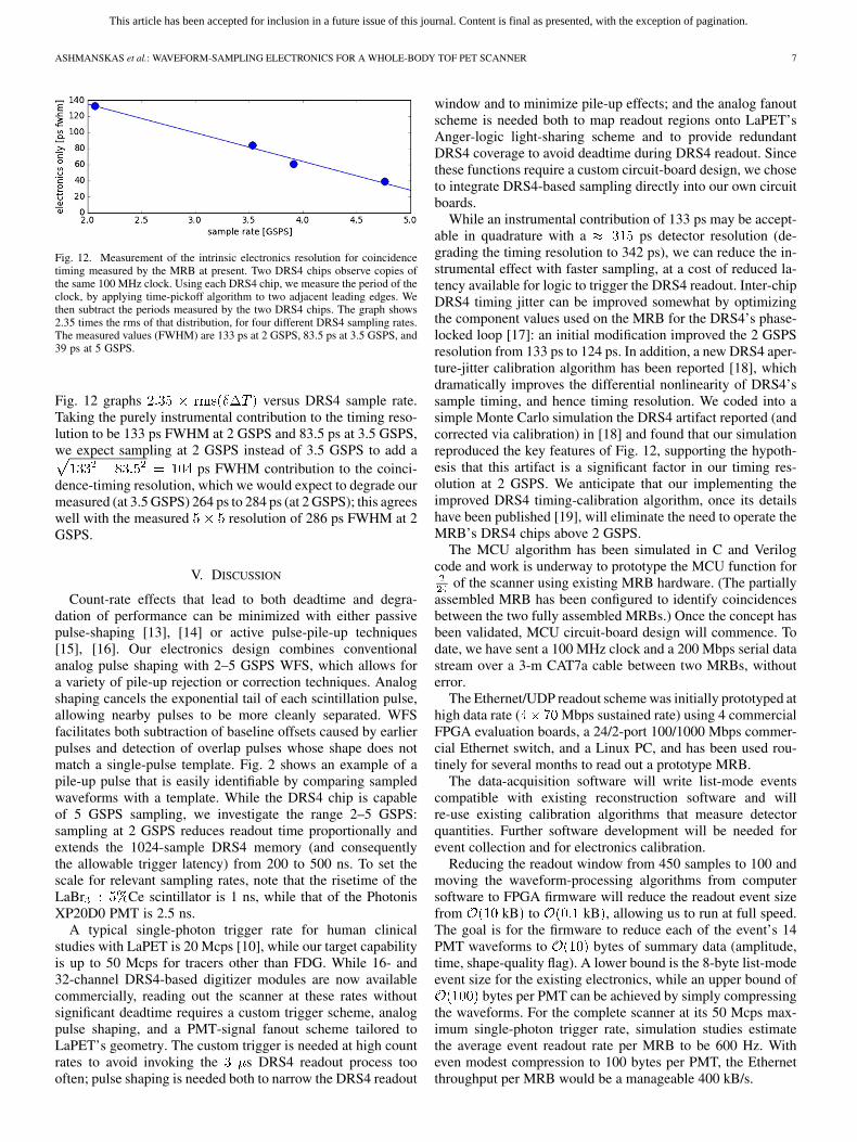
Fig. 12. Measurement of the intrinsic electronics resolution for coincidencetiming measured by the MRB at present. Two DRS4 chips observe copies ofthe same 100 MHz clock. Using each DRS4 chip, we measure the period of theclock, by applying time-pickoff algorithm to two adjacent leading edges. Wethen subtract the periods measured by the two DRS4 chips. The graph shows2.35 times the rms of that distribution, for four different DRS4 sampling rates.The measured values (FWHM) are 133 ps at 2 GSPS, 83.5 ps at 3.5 GSPS, and39 ps at 5 GSPS.
Fig. 12 graphs versus DRS4 sample rate.Taking the purely instrumental contribution to the timing reso-lution to be 133 ps FWHM at 2 GSPS and 83.5 ps at 3.5 GSPS,we expect sampling at 2 GSPS instead of 3.5 GSPS to add a
ps FWHM contribution to the coinci-dence-timing resolution, which we would expect to degrade ourmeasured (at 3.5 GSPS) 264 ps to 284 ps (at 2 GSPS); this agreeswell with the measured resolution of 286 ps FWHM at 2GSPS.
V. DISCUSSION
Count-rate effects that lead to both deadtime and degra-dation of performance can be minimized with either passivepulse-shaping [13], [14] or active pulse-pile-up techniques[15], [16]. Our electronics design combines conventionalanalog pulse shaping with 2–5 GSPS WFS, which allows fora variety of pile-up rejection or correction techniques. Analogshaping cancels the exponential tail of each scintillation pulse,allowing nearby pulses to be more cleanly separated. WFSfacilitates both subtraction of baseline offsets caused by earlierpulses and detection of overlap pulses whose shape does notmatch a single-pulse template. Fig. 2 shows an example of apile-up pulse that is easily identifiable by comparing sampledwaveforms with a template. While the DRS4 chip is capableof 5 GSPS sampling, we investigate the range 2–5 GSPS:sampling at 2 GSPS reduces readout time proportionally andextends the 1024-sample DRS4 memory (and consequentlythe allowable trigger latency) from 200 to 500 ns. To set thescale for relevant sampling rates, note that the risetime of theLaBr Ce scintillator is 1 ns, while that of the PhotonisXP20D0 PMT is 2.5 ns.
A typical single-photon trigger rate for human clinicalstudies with LaPET is 20 Mcps [10], while our target capabilityis up to 50 Mcps for tracers other than FDG. While 16- and32-channel DRS4-based digitizer modules are now availablecommercially, reading out the scanner at these rates withoutsignificant deadtime requires a custom trigger scheme, analogpulse shaping, and a PMT-signal fanout scheme tailored toLaPET’s geometry. The custom trigger is needed at high countrates to avoid invoking the s DRS4 readout process toooften; pulse shaping is needed both to narrow the DRS4 readout
window and to minimize pile-up effects; and the analog fanoutscheme is needed both to map readout regions onto LaPET’sAnger-logic light-sharing scheme and to provide redundantDRS4 coverage to avoid deadtime during DRS4 readout. Sincethese functions require a custom circuit-board design, we choseto integrate DRS4-based sampling directly into our own circuitboards.
While an instrumental contribution of 133 ps may be accept-able in quadrature with a ps detector resolution (de-grading the timing resolution to 342 ps), we can reduce the in-strumental effect with faster sampling, at a cost of reduced la-tency available for logic to trigger the DRS4 readout. Inter-chipDRS4 timing jitter can be improved somewhat by optimizingthe component values used on the MRB for the DRS4’s phase-locked loop [17]: an initial modification improved the 2 GSPSresolution from 133 ps to 124 ps. In addition, a new DRS4 aper-ture-jitter calibration algorithm has been reported [18], whichdramatically improves the differential nonlinearity of DRS4’ssample timing, and hence timing resolution. We coded into asimple Monte Carlo simulation the DRS4 artifact reported (andcorrected via calibration) in [18] and found that our simulationreproduced the key features of Fig. 12, supporting the hypoth-esis that this artifact is a significant factor in our timing res-olution at 2 GSPS. We anticipate that our implementing theimproved DRS4 timing-calibration algorithm, once its detailshave been published [19], will eliminate the need to operate theMRB’s DRS4 chips above 2 GSPS.
The MCU algorithm has been simulated in C and Verilogcode and work is underway to prototype the MCU function for
of the scanner using existing MRB hardware. (The partiallyassembled MRB has been configured to identify coincidencesbetween the two fully assembled MRBs.) Once the concept hasbeen validated, MCU circuit-board design will commence. Todate, we have sent a 100 MHz clock and a 200 Mbps serial datastream over a 3-m CAT7a cable between two MRBs, withouterror.
The Ethernet/UDP readout scheme was initially prototyped athigh data rate ( Mbps sustained rate) using 4 commercialFPGA evaluation boards, a 24/2-port 100/1000 Mbps commer-cial Ethernet switch, and a Linux PC, and has been used rou-tinely for several months to read out a prototype MRB.
The data-acquisition software will write list-mode eventscompatible with existing reconstruction software and willre-use existing calibration algorithms that measure detectorquantities. Further software development will be needed forevent collection and for electronics calibration.
Reducing the readout window from 450 samples to 100 andmoving the waveform-processing algorithms from computersoftware to FPGA firmware will reduce the readout event sizefrom kB to kB , allowing us to run at full speed.The goal is for the firmware to reduce each of the event’s 14PMT waveforms to bytes of summary data (amplitude,time, shape-quality flag). A lower bound is the 8-byte list-modeevent size for the existing electronics, while an upper bound of
bytes per PMT can be achieved by simply compressingthe waveforms. For the complete scanner at its 50 Mcps max-imum single-photon trigger rate, simulation studies estimatethe average event readout rate per MRB to be 600 Hz. Witheven modest compression to 100 bytes per PMT, the Ethernetthroughput per MRB would be a manageable 400 kB/s.

This article has been accepted for inclusion in a future issue of this journal. Content is final as presented, with the exception of pagination.
8 IEEE TRANSACTIONS ON NUCLEAR SCIENCE
Once we have moved the processing (or at least pre-pro-cessing) of DRS4 waveforms from software into FPGAfirmware and adapted our present benchtop tests to find coinci-dences between two separate MRBs (with a third MRB servingto prototype the MCU function), our next milestone will be touse these three boards to read out two modules of the LaPETscanner. Finally, a dedicated MCU board and a production runof MRB circuit boards will be fabricated to instrument a largerfraction of the scanner.
VI. SUMMARY
We have demonstrated that WFS retains the intrinsic pre-cision of timing information of the scintillation signal, andhave achieved 315 ps (FWHM coincidence timing resolu-tion) for a test array of LaBr crystals with a new design ofelectronics. These electronics can be scaled to our prototypeLaPET scanner, and should enable us to achieve similar timingperformance. We currently experience some losses in timingperformance with LaPET, which uses more conventionalelectronics, so that in practice we achive a system timingresolution between 375–420 ps, depending on the count rateof the study. Some care will be needed to optimize both thesampling rate and the number of samples read out, e.g., forbaseline correction, for energy measurement, and for pile-updetection. One challenge in scaling from a small detector on abenchtop to a whole-body TOF PET scanner is the control ofchannel-to-channel gain and timing offsets. A key challengein operating a whole-body TOF PET scanner at high countrate (20–50 Mcps single-photon trigger rate) is to preserveexcellent timing, energy, and position resolution in the presenceof pile-up interactions. Our electronics design addresses thesechallenges. By processing individual PMT signals digitally, wemaximize available handles for controlling calibration effects.Using high-speed waveform sampling facilitiates our handlingbaseline offsets and pile-up pulses at count rates pertinent forpatient imaging. We are currently testing prototypes of thecircuit boards with which we will re-instrument the LaPETwhole-body prototype scanner. While the modules we havedesigned are tailored to LaPET’s geometry, the concept can bereadily adapted to other detector configurations.
REFERENCES
[1] W. W. Moses, S. Buckley, C. Vu, Q. Peng, N. Pavlov, W. S. Choong,J. Wu, and C. Jackson, “OpenPET: A flexible electronics systemfor radiotracer imaging,” IEEE Trans. Nucl. Sci., vol. 57, no. 5, pp.2532–2537, Oct. 2010.
[2] M. Conti, B. Bendriem, M. Casey, L. Eriksson, B. Jakoby, W. F. Jones,J. Jones, C. Michel, C. Nahmias, V. Panin, V. Rappoport, M. Sibomana,and D. W. Townsend, “Performance of a high sensitivity PET scannerbased on LSO panel detectors,” IEEE Trans. Nucl. Sci., vol. 53, no. 3,pp. 1136–1142, Jun. 2006.
[3] M. S. Musrock, J. W. Young, J. C. Moyers, J. E. Breeding, M. E. Casey,J. M. Rochelle, D. M. Binkley, and B. K. Swann, “Performance char-acteristics of a new generation of processing circuits for PET applica-tions,” IEEE Trans. Nucl. Sci., vol. 50, no. 4, pp. 974–978, Aug. 2003.
[4] W. W. Moses, J. W. Young, K. Baker, W. Jones, M. Lenox, M. H. Ho,and M. Weng, “The electronics system for the LBNL Positron EmissionMammography (PEM) camera,” IEEE Trans. Nucl. Sci., vol. 48, no. 3,pp. 632–636, Jun. 2001.
[5] S. Ritt, R. Dinapoli, and U. Hartmann, “Application of the DRS chipfor fast waveform digitizing,” Nucl. Instr. Meth., vol. A623, p. 486,2010.
[6] A. Ronzhin, M. Albrow, S. Los, M. Martens, P. Murat, E. Ramberg, H.Kim, C. T. Chen, C. M. Kao, K. Niessen, A. Zatserklyaniy, M. Mazz-illo, B. Carbone, G. Condorelli, G. Fallica, A. Piana, D. Sanfilippo, G.Valvo, and S. Ritt, “A SiPM-based TOF-PET detector with high speeddigital DRS4 readout,” Nucl. Instr. Meth., vol. A703, p. 109, 2013.
[7] K. S. Shah, J. Glodo, M. Klugerman, W. W. Moses, S. E. Derenzo,and M. J. Weber, “LaBr :Ce scintillators for gamma-ray spectroscopy,”IEEE Trans. Nucl. Sci., vol. 50, no. 6, pp. 2410–2413, Dec. 2003.
[8] A. Kuhn, S. Surti, J. S. Karp, G. Muehllehner, F. M. Newcomer, and R.Van Berg, “Performance assessment of pixelated LaBr detector mod-ules for time-of-flight PET,” IEEE Trans. Nucl. Sci., vol. 53, no. 3, pp.1090–1095, Jun. 2006.
[9] C. C. M. Kyba, R. I. Wiener, F. M. Newcomer, A. E. Perkins, R. R.Kulp, M. E. Werner, S. Surti, N. Dressandt, R. Van Berg, and J. S.Karp, “Evaluation of local PMT triggering electronics for a TOF-PETscanner,” in Proc. 2008 IEEE Nucl. Science Symp. and MedicalImaging Conf. (NSS/MIC), pp. 4608–4613.
[10] M. E. Daube-Witherspoon, S. Surti, A. Perkins, C. C. M. Kyba, R.Wiener, M. E. Werner, R. Kulp, and J. S. Karp, “The imaging perfor-mance of a LaBr -based PET scanner,” Phys. Med. Biol., vol. 55, p. 45,2010.
[11] J. F. Genat, G. Varner, F. Tang, and H. Frisch, “Signal processing forpico-second resolution timing measurements,” Nucl. Instr. Meth., vol.A607, p. 387, 2009.
[12] Z. S. Davidson, R. I. Wiener, F. M. Newcomer, R. Van Berg, and J.S. Karp, “High voltage photodetector calibration for improved timingresolution with scintillation detectors for TOF-PET imaging,” in Proc.2011 IEEE Nuclear Science Symp. Medical Imaging Conf. (NSS/MIC),pp. 2338–2341.
[13] J. S. Karp, D. A. Mankoff, and G. Muehllehner, “A position-sensitivedetector for use in positron emission tomography,” Nucl. Instr. Meth.,vol. A273, p. 891, 1988.
[14] R. Freifelder, J. S. Karp, J. A. Wear, N. S. Lockyer, F. M. Newcomer, S.Surti, and R. Van Berg, “Comparison of multi-pole shaping and delayline clipping pre-amplifiers for position sensitive NaI(Tl) detectors,”IEEE Trans. Nucl. Sci., vol. 45, no. 3, pp. 1138–1143, Jun. 1998.
[15] W. H. Wong and H. Li, “A scintillation detector signal processing tech-nique with active pileup prevention for extending scintillation countrates,” IEEE Trans. Nucl. Sci., vol. 45, no. 3, pp. 838–842, Jun. 1998.
[16] E. Tanaka, T. Ohmura, and T. Yamashita, “A new method for pre-venting pulse pileup in scintillation detectors,” Phys. Med. Biol., vol.47, p. 327, 2002.
[17] S. Ritt, private communication.[18] D. Stricker-Shaver, “Comparison between DRS4 chip-based boards
and a 2 GS/s-ADC for a flexible PET electronics,” presented at the2012 IEEE NSS/MIC Conf., 2012, Oral Presentation M11-4.
[19] D. A. Stricker-Shaver, S. Ritt, and B. J. Pichler, “Novel calibrationmethod for DRS4-Chip enables 3 ps time resolution measurements,”presented at the 2013 IEEE NSS/MIC Conf., 2013, Oral PresentationN21-2.