ieee transactions on electron devices, vol. … · performance of a lateral insulated-gate bipolar...
TRANSCRIPT

IEEE TRANSACTIONS ON ELECTRON DEVICES, VOL. 60, NO. 12, DECEMBER 2013 4185
Effect of Bandgap Narrowing on Performanceof Modern Power Devices
Gianluca Camuso, Ettore Napoli, Vasantha Pathirana, Nishad Udugampola,Alice Pei-Shan Hsieh, Tanya Trajkovic, and Florin Udrea
Abstract— The effect of the bandgap narrowing (BGN) onperformance of power devices is investigated in detail in thispaper. The analysis reveals that the change in the energy bandstructure caused by BGN can strongly affect the conductivitymodulation of the bipolar devices resulting in a completely differ-ent performance. This is due to the modified injection efficiencyunder high-level injection conditions. Using a comprehensiveanalysis of the injection efficiency in a p-n junction, an analyticalmodel for this phenomenon is developed. BGN model tuninghas been proved to be essential in accurately predicting theperformance of a lateral insulated-gate bipolar transistor (IGBT).Other devices such as p-i-n diodes or punch-through IGBTs aresignificantly affected by the BGN, while others, such as field-stopIGBTs or power MOSFETs, are only marginally affected.
Index Terms— Bandgap narrowing, insulated-gate bipolartransistor (IGBT), power devices, high voltage.
I. INTRODUCTION
F INITE element device simulators are widely employedin power device research and development to predict
device behavior and to avoid relying on extensive experi-mental analysis which can be costly and time consuming.In order to achieve good matching with fabricated deviceperformance, the simulation models must be properly selectedand tuned. However, with dozens of models available inmodern simulators and complex physical phenomena occur-ring at different modes of operation (static, dynamic, andtemperature dependent), it is difficult to identify the mostadequate combination of models without understanding theunderlying physics responsible for device behavior.
One of the critical models that need to be adjusted is relatedto the bandgap narrowing (BGN) effect [1] which can play animportant role in highly doped regions of the semiconductor.Different techniques have been adopted to measure the BGN
Manuscript received January 24, 2013; revised October 3, 2013; acceptedOctober 4, 2013. Date of current version November 20, 2013. This work wassupported by the U.K. Power Electronics Centre under Grant EP/L007010/1.The review of this paper was arranged by Editor G. Dolny.
G. Camuso and A. P.-S. Hsieh are with the Department of Engineering,Cambridge University, Cambridge CB21PZ, U.K. (e-mail: [email protected];[email protected]).
E. Napoli is with DIBET, University of Napoli Federico II, Naples 80125,Italy (e-mail: [email protected]).
V. Pathirana, N. Udugampola, and T. Trajkovic are with CambridgeMicroelectronics Ltd., Cambridge CB30FA, U.K. (e-mail:[email protected]; [email protected];[email protected]).
F. Udrea is with the Department of Engineering, Cambridge University,Cambridge CB21PZ, U.K., and also with the Cambridge MicroelectronicsLtd., Cambridge CB30FA, U.K. (e-mail: [email protected]).
Digital Object Identifier 10.1109/TED.2013.2286528
but they refer to specific materials (i.e., epitaxial layer [2]),specific device properties (e.g., β in a bipolar transistor [3]),or they employ approximations (e.g., low injection, uniformdoping [4], [5]). The effect of BGN on the performance ofthe bipolar junction transistors is well known and has beenintensively analyzed in the past [6], [7]. More recently, BGNanalysis has been mostly carried out for new materials, suchas GaAs [8], or those used in solar cells [9]. However, thereare no published reports on the effect of the BGN on modernpower devices such as p-i-n Diodes, MOSFETs, and insulated-gate bipolar transistors (IGBTs). The aim of this paper is toinvestigate the effect of BGN on these devices. In the firstpart of this paper, we examine analytically how BGN affectsthe physics of bipolar power devices. This is followed by theanalysis showing in which cases it is important to use theBGN model to achieve high simulation accuracy. Finally, wepresent the case of how a well-tuned BGN model is used insimulations to model a commercial lateral IGBT.
2-D simulations are used to understand and explain thedifferent behavior of devices with respect to the BGN effect.The numerical analysis software used to carry out this paper isSentaurus Device [10]. However, other commercially availablefinite element methods (FEMs), such as Medici or Silvaco, canbe employed for a similar analysis.
II. BANDGAP NARROWING MODEL
In Sentaurus Device, the bandgap of a material is definedas
Eg_eff = Eg_0 + δEg − αT 2
T + β− �EBGN − �EFermi
BGN (1)
where T is the absolute temperature, α and β are temper-ature coefficients, and Eg_0 and δEg define the bandgap atT = 0 K.
�EBGN is the BGN component calculated using theMaxwell–Boltzmann statistic [11], and �EFermi
BGN is the addi-tional component used if Fermi statistic [10] is considered inthe analysis. For the devices analyzed in this paper, wheredoping levels do not exceed 1 × 1019 cm−3, Fermi–Diracdistribution is not necessary; so only the Maxwell–Boltzmannstatistic has been used
(�EFermi
BGN = 0)
[12]. Sentaurus FEMsimulator can use different BGN models to calculate �EBGN:e.g., Slotboom, Bennett, del Alamo, and Jain–Roulston. Select-ing a specific BGN model does not present a limitation for thisanalysis since the difference between models will be reflectedonly in the final value of �EBGN, while the focus of this paper
0018-9383 © 2013 IEEE

4186 IEEE TRANSACTIONS ON ELECTRON DEVICES, VOL. 60, NO. 12, DECEMBER 2013
is on explaining its effect irrespective of the absolute value.The study presented in this paper has been carried out usingthe Slotboom model [13], given by
�EBGN = Eref
[
In[ Ntot
Nref
]+
√[In
[Ntot
Nref
]]2 + 0.5
]
(2)
where Eref and Nref are, respectively, 6.92 × 10⁻³ eV and1.3 × 1017 cm−3. The default model considers Ntot as the netdoping concentration, although analysis with carrier-dependentbandgap can also be found in the literature [14]. However, thisapproach is difficult to implement in simulations because ofserious convergence problems. Moreover, the literature reportssignificant difference in device performance when currentdensities exceed 10 000 A/cm−2. This is well outside theoperating area for power devices. For example, MOSFETstypically operate in the ON-state at 20–50 A/cm−2, whileIGBTs can go up to 100–250 A/cm−2. Even during short-circuit conditions when IGBTs are in saturation, the currentdensities do not exceed 1000 A/cm−2.
III. ANALYSIS OF THE BGN EFFECT USING
ANALYTICAL MODELING
It is well known that BGN affects only bipolar structures.To gain a better understanding of device physics and how itis affected by BGN, we start by analytically investigating ap+/n– junction for two conditions.
1) BGN Effect is taken into account for the p+ region,indicated as “With BGN.”
2) BGN Effect is not considered, indicated as “WithoutBGN.”
A. Junction at Equilibrium
With both terminals grounded, the main difference betweenthe “With BGN” and “Without BGN” cases is the effectiveintrinsic carrier concentration nipeff for the p region. To satisfythe mass-action law at the equilibrium
n2ipeff
= ni · e�Ebgn
K ·T = n P0 · PP0 (3)
n p0 has to change since pp0 is fixed by the acceptor doping.Therefore, the higher minority carrier concentration results ina lower built-in potential Vbi and a higher saturation currentIs [11] for the case “With BGN.”
B. Junction Outside Equilibrium
By applying a voltage Va to the anode, the junction is ina low-level current injection mode. The voltage across thedepletion region, V ∗
a , is the same as Va . By increasing Va ,the current across the device increases and the structure entersthe high injection regime. Unlike in the previous case, V ∗
a isnot equivalent to Va anymore because the high current levelgenerates additional voltage drop both across the contacts andin the cathode region. In this regime, the expression for V ∗
a is
V ∗a = Va − Rk · I (4)
where Rk is the resistance of the cathode region.
The high injection current condition is reached at a lowervoltage Va for the case “With BGN” because of the lower Vbiand higher Is, as discussed above.
In the high injection condition, it is reasonable to assumethat the minority excess carrier density for the n region andthe p region are equal (δpn = δn p). Considering Boltzmannequations [1], it is possible to derive δpn as
δPn = ND
2
⎡
⎢⎢⎣
√√√√√1 +
4 · n2i ·
(e
VaVt − 1
)
N2D
− 1
⎤
⎥⎥⎦
∼= n2i · e
V a∗2·V t . (5)
For the same current density, a lower V ∗a will result in an
exponentially lower injection of carriers (in this case holesfrom the p+ region into the n region), leading to a higherresistivity of the n layer (hence higher Rk). As a consequence,the plasma concentration in the n region will be lower for thecase “With BGN” for any fixed current density. It is importantto note that a more prominent difference between the twocases (“With BGN” and “Without BGN”) would be observedif the BGN effect is also taken into account for the n region.This is because the increase in the effective intrinsic carrierconcentration nineff will lead to a bigger difference in Vbi andIs between the two conditions analyzed.
It is evident from the analysis above that the BGN can affectVbi, which is an important parameter for the performanceof bipolar power devices, thereby clearly indicating that itshould be carefully considered for modeling and simulationof these structures. Since most power devices operate atelevated junction temperatures, it is important to investigate theinfluence of the BGN effect under those conditions. From (3)it can be expected that nipeff will be closer to ni at highertemperatures, which will result in a less prominent effect ofBGN on Vbi.
IV. EFFECT OF BGN ON POWER DEVICES
We have studied several different power devices in orderto explain how the theory presented in the previous sectionapplies to more complex structures. All simulations usedthe Philips Unified model for mobility, Shockley ReadHall and Auger recombination models, and for the cases“With BGN,” the Slotboom bandgap narrowing model isapplied to all regions in the structure. Because of spacelimitation, we focus here on the ON-state performance analysisat different temperatures, although it is reasonable to assumethat the changes in the ON-state will also result in modifiedswitching characteristics.
A. p-i-n Diode
p-i-n diodes are still very popular and widely used in powerelectronic applications such as power rectifiers, protection cir-cuits, and for clamped inductive switching. The cross sectionand the doping profiles of the structure simulated are shown inFig. 1. The carrier lifetime used in simulations was 1 μs; thedoping concentration and temperature-dependent degradationwere also enabled.

CAMUSO et al.: EFFECT OF BGN ON THE PERFORMANCE OF MODERN POWER DEVICES 4187
Fig. 1. Cross section and doping profile of the simulated p-i-n diode.
Fig. 2. Comparison of simulated ON-state characteristics for a p-i-n diode“With BGN” and “Without BGN.”
The ON-state comparison at 25 °C and 125 °C for thesimulations “With BGN” and “Without BGN” is presentedin Fig. 2. As expected from the analysis of Vbi in Section III,the device simulated “With BGN” starts conducting for a loweranode voltage than “Without BGN.” On the other hand, in thehigh injection regime, the simulation “With BGN” exhibitsa lower current density becauseof the weaker injection. Thecombination of this two effects results in the intersection ofthe curves (crossover point). as shown in Fig. 2.
Comparing the device performance at 25 °C and 125 °C, it isclear that the effect of BGN is reduced at higher temperatures.It is important to note that in the high injection regime,where (4) applies, Rk increases with temperature because ofthe reduced mobility which results in a larger difference incurrent density between the simulations with and without theBGN model.
B. Punch-Through IGBT
IGBTs are very popular because of their high current den-sities and tunable trade-off between conduction and switchinglosses. Although less popular than the better performing field-stop (FS) IGBTs (see Section IV-C), punch-through (PT)IGBTs are still widely used in relatively low-frequency (below10 KHz) power electronics applications because of their lowercost and easier fabrication. Half-cell cross section of thesimulated 600 V rated PT trench IGBT and the doping profilealong X = 1 μm are shown in Fig. 3. The lifetime used forthese simulations was 0.1 μs. The threshold voltage is 4 V,
Fig. 3. Cross section and doping profile of the simulated PT IGBT cell.
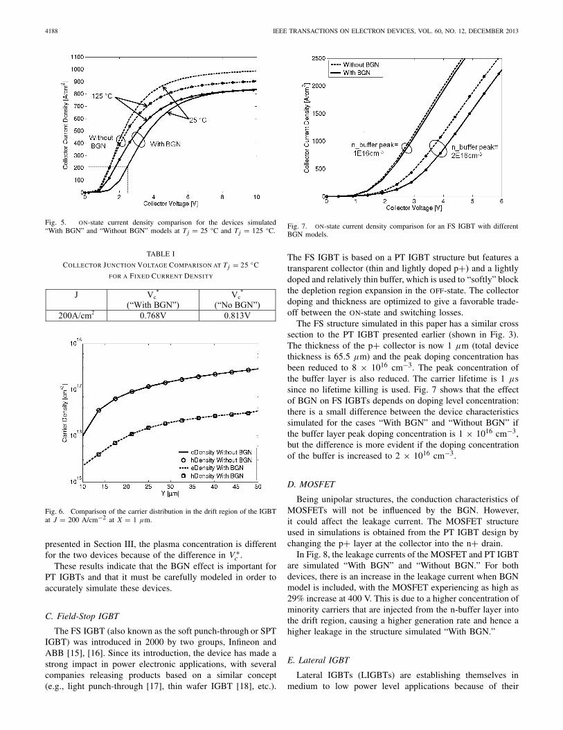
Fig. 4. ON-state current density comparison at 25 °C for the devices simulated“With BGN” and “Without BGN” models.
and in the ON-state the device is operated with Vg = 15 V.Fig. 4 shows simulated ON-state current densities obtained“With BGN” and “Without BGN” at 25 °C. Similar to whatwas observed for the p-i-n diode, different injection levels ofthe collector p-n junction create the crossover point.
Full I–V characteristics given in Fig. 5 show that thedevice “With BGN” has a larger ON-state voltage drop (VON)for the same operating current density (e.g., 200 A/cm−2).This behavior can be explained by analyzing the plasmaconcentration of the two structures.
Table I shows a comparison of the voltage across thecollector junction (V ∗
c , which is equivalent to V ∗a discussed
in the p-n junction section) for a fixed current densityJ = 200 A/cm−2 obtained for the structures “With BGN”and “Without BGN.”
In high injection regime, the voltage across the collectorjunction for the same current density will be lower for thestructure “With BGN” because of the increase in Vbi. This willresult in a lower conductivity modulation of the drift region.This is confirmed in Fig. 6, which shows the comparison ofthe 1-D carrier distribution in the drift region (200 A/cm−2,X = 1 μm) for the two cases, namely “With BGN” and“Without BGN.” As expected from the analytical modeling
4188 IEEE TRANSACTIONS ON ELECTRON DEVICES, VOL. 60, NO. 12, DECEMBER 2013
Fig. 5. ON-state current density comparison for the devices simulated“With BGN” and “Without BGN” models at Tj = 25 °C and Tj = 125 °C.
TABLE I
COLLECTOR JUNCTION VOLTAGE COMPARISON AT Tj = 25 °C
FOR A FIXED CURRENT DENSITY
Fig. 6. Comparison of the carrier distribution in the drift region of the IGBTat J = 200 A/cm−2 at X = 1 μm.
presented in Section III, the plasma concentration is differentfor the two devices because of the difference in V ∗
c .These results indicate that the BGN effect is important for
PT IGBTs and that it must be carefully modeled in order toaccurately simulate these devices.
C. Field-Stop IGBT
The FS IGBT (also known as the soft punch-through or SPTIGBT) was introduced in 2000 by two groups, Infineon andABB [15], [16]. Since its introduction, the device has made astrong impact in power electronic applications, with severalcompanies releasing products based on a similar concept(e.g., light punch-through [17], thin wafer IGBT [18], etc.).
Fig. 7. ON-state current density comparison for an FS IGBT with differentBGN models.
The FS IGBT is based on a PT IGBT structure but features atransparent collector (thin and lightly doped p+) and a lightlydoped and relatively thin buffer, which is used to “softly” blockthe depletion region expansion in the OFF-state. The collectordoping and thickness are optimized to give a favorable trade-off between the ON-state and switching losses.
The FS structure simulated in this paper has a similar crosssection to the PT IGBT presented earlier (shown in Fig. 3).The thickness of the p+ collector is now 1 μm (total devicethickness is 65.5 μm) and the peak doping concentration hasbeen reduced to 8 × 1016 cm−3. The peak concentration ofthe buffer layer is also reduced. The carrier lifetime is 1 μssince no lifetime killing is used. Fig. 7 shows that the effectof BGN on FS IGBTs depends on doping level concentration:there is a small difference between the device characteristicssimulated for the cases “With BGN” and “Without BGN” ifthe buffer layer peak doping concentration is 1 × 1016 cm−3,but the difference is more evident if the doping concentrationof the buffer is increased to 2 × 1016 cm−3.
D. MOSFET
Being unipolar structures, the conduction characteristics ofMOSFETs will not be influenced by the BGN. However,it could affect the leakage current. The MOSFET structureused in simulations is obtained from the PT IGBT design bychanging the p+ layer at the collector into the n+ drain.
In Fig. 8, the leakage currents of the MOSFET and PT IGBTare simulated “With BGN” and “Without BGN.” For bothdevices, there is an increase in the leakage current when BGNmodel is included, with the MOSFET experiencing as high as29% increase at 400 V. This is due to a higher concentration ofminority carriers that are injected from the n-buffer layer intothe drift region, causing a higher generation rate and hence ahigher leakage in the structure simulated “With BGN.”
E. Lateral IGBT
Lateral IGBTs (LIGBTs) are establishing themselves inmedium to low power level applications because of their
CAMUSO et al.: EFFECT OF BGN ON THE PERFORMANCE OF MODERN POWER DEVICES 4189
Fig. 8. Simulated leakage current comparison for a PT IGBT and theequivalent MOSFET at 125 °C.
Fig. 9. Cross section of the simulated LIGBT structure that has beendeveloped and used in Camsemi products.
enhanced current density capability when compared to equiv-alent lateral MOSFETs. A new lateral 800 V rated bulk SiLIGBT has been recently developed by Camsemi and used inlarge volume products for low-power switched-mode powersupply (SMPS) applications [19]. The cross section of thisdevice, which has been used in the final section of our BGNanalysis, is shown in Fig. 9.
Fig. 10 shows the comparison of simulated ON-state char-acteristics for the LIGBT “With BGN” and “Without BGN.”It is evident that this device is extremely sensitive to theBGN. Since the device is fabricated with a CMOS-basedprocess, the p+ implantation dose is well above the levelat which BGN starts to be significant (this corresponds to apeak concentration of 1 × 1017 cm−3). In addition, also the nbuffer is realized with a high concentration of dopant in orderto control the injection efficiency. From Fig. 10, it is clearthat the device characteristics are less affected by the BGNeffect at Tj = 125 °C (i.e., the effect is more prominent atTj = 25 °C). This is consistent with the analysis presented inSection III (3).
V. EXPERIMENTAL VALIDATION AND TUNING
OF THE MODEL
In Section IV-E, we showed how important it is to considerthe BGN effect in simulating the behavior of the LIGBT.
Fig. 10. ON-state current comparison for a lateral IGBT with and withoutthe BGN model.
Fig. 11. Comparison between simulations and measurements at 25 °C and125 °C for ON-state of the LIGBT with different BGN models.
Fig. 12. Comparison between simulations and measurements at 25 °C and125 °C for turn-off of the LIGBT.
In this section, we bring further evidence that that the TCADmodel has to be properly set in order to achieve good matchingwith the fabricated device performance. Fig. 11 shows thecomparison between measurements and equivalent simulationswith different BGN models. It is clear that for the fine-tuningof the simulation models, which is required to achieve goodmatching with the fabricated device, it is necessary to selectthe most adequate BGN model.

4190 IEEE TRANSACTIONS ON ELECTRON DEVICES, VOL. 60, NO. 12, DECEMBER 2013
Tuning of the lifetime and mobility models is also impor-tant but these alone, without applying an appropriate BGNmodel, did not allow achieving a satisfactory result in all thedifferent conditions of operations (ON-state and transient atdifferent temperature). The introduction and fine-tuning of theBGN model ensured a significantly more precise matching.In particular, we found that the best match for the LIGBTdeveloped by Camsemi was achieved using the BGN modelusually referred to in the literature as the “Old Slotboom.”For completeness of the analysis, a comparison betweensimulations and measurement for the turn-off of the device isshown in Fig. 12 (clamped inductive switching configuration).
VI. CONCLUSION
In this paper, we investigated the BGN effect on the perfor-mance of several power devices. The analyses demonstratedthat a difference in the bandgap due to the doping of the p-njunction at the anode side of p-i-n diodes and the collector ofPT IGBTs and LIGBTs heavily affects the device performanceduring ON-state conduction. The injection efficiency of thedevice can change significantly because of the change in thebuilt-in potential across the p-n junction during forward bias.This, in turn, affects the conductivity modulation of the driftregion. We conclude that the effect of the BGN decreases withtemperature and it is less prominent for the FS IGBT structurebecause of the lower doping concentration. The leakage currentof all the devices investigated is affected by BGN because ofthe different minority carrier concentration which modifies thegeneration–recombination rate. Finally, we have found that,for a lateral IGBT, the model referred to as “Old Slotboom”gives a more accurate fit than the more recently favored“New Slotboom” or “Bennett” models, and for this reason werecommend using this as a starting point for a more accurateTCAD platform.
ACKNOWLEDGMENT
The authors would like to thank M. Antoniou,G. Longobardi, and N. Lophitis for helpful discussions.
REFERENCES
[1] B. Baliga, Fundamentals of Power Semiconductor Devices. New York,NY, USA: Springer-Verlag, 1996, pp. 29–33.
[2] J. del Alamo, R. Swirhun, and M. Swanson, “Simultaneous measurementof hole lifetime, hole mobility and bandgap narrowing in heavily dopedn-type silicon,” in Proc. IEDM, 1985, pp. 290–293.
[3] J. W. Slotboom and H. C. De Graaff, “Measurements of bandgapnarrowing in Si bipolar transistors,” Solid-State Electron., vol. 19, no. 10,pp. 857–862, 1976.
[4] R. P. Mertens, J. L. Van Meerbergen, J. F. Nijs, and R. J. VanOverstraeten, “Measurement of the minority-carrier transport parametersin heavily doped silicon,” IEEE Trans. Electron Devices, vol. 27, no. 5,pp. 949–955, May 1980.
[5] A. W. Wieder, “Emitter effects in shallow bipolar devices measurementsand consequences,” IEEE Trans. Electron Devices, vol. 27, no. 8,pp. 1402–1408, Aug. 1980.
[6] M. S. Mock, “Transport equations in heavily doped silicon, and thecurrent gain of a bipolar transistor,” Solid-State Electron., vol. 16, no. 11,pp. 1251–1259, 1973.
[7] H. J. De Man, “The influence of heavy doping on the emitter efficiencyof a bipolar transistor,” IEEE Trans. Electron Devices, vol. 18, no. 10,pp. 833–835, Oct. 1971.
[8] S. C. Jain, J. M. McGregor, D. J. Roulston, and P. Balk, “Modifiedsimple expression for bandgap narrowing in n-type GaAs,” Solid-StateElectron., vol. 35, no. 5, pp. 639–642, 1992.
[9] P. Nubile and A. Ferreira da Silva, “Bandgap narrowing in siliconsolar cells considering the p-type doping material,” Solid-State Electron.,vol. 41, no. 1, pp. 121–124, 1997.
[10] Sentaurus Device User Guide. New York, NY, USA: Springer-Verlag,Dec. 2007.
[11] S. M. Sze, Physics of Semiconductor Devices. New York, NY, USA:Wiley, 2007.
[12] D. L. Pulfrey, Modern Transistors and Diodes. Cambridge, U.K.:Cambridge University Press, 2010.
[13] J. W. Slotboom and H. C. De Graaff, “Bandgap narrowing in sili-con bipolar transistor,” IEEE Trans. Electron Devices, vol. 24, no. 8,pp. 1123–1125, Aug. 1977.
[14] Y. J. Park, R. K. Cook, and S. P. Gaur, “The effects of carrier-concentration-dependent bandgap narrowing on bipolar-device charac-teristics,” IEEE Trans. Electron Devices, vol. 32, no. 5, pp. 874–876,May 1985.
[15] T. Laska, “The field stop IGBT FS IGBT—A new power device conceptwith great improvement potential,” in Proc. ISPSD, 2000, pp. 1–335.
[16] S. Dewar, “Soft punch through SPT—Setting new standards in 1200VIGBT,” in Proc. PCIM, 2000, pp. 1–593.
[17] K. Nakamura, S. Kusunoki, H. Nakamura, Y. Ishimura, Y. Tomomatsu,and T. Minato, “Advanced wide cell pitch CSTBTs having light punchthrough (LPT) structures,” in Proc. ISPSD, 2002, pp. 277–280.
[18] J. Vobecký, M. Rahimo, A. Kopta, and S. Linder, “Exploring the silicondesign limits of thin wafer IGBT technology: The controlled punchthrough (CPT) IGBT,” in Proc. ISPSD, 2008, pp. 76–79.
[19] T. Trajkovic, V. Pathirana, N. Udugampola, G. Camuso, F. Udrea, andG. Amaratunga, “800V LIGBT in bulk Si for low power compact SMPSapplications,” in Proc. ISPSD, 2013, pp. 401–404.
Gianluca Camuso received the M.Sc. degree in electrical engineering fromthe University of Naples, Naples, Italy, in 2010. He is currently pursuingthe Ph.D. degree with the High Voltage Microelectronics and Sensors Lab,Department of Engineering, University of Cambridge, Cambridge, U.K.
Ettore Napoli received the Ph.D. degree in electronic engineering in 1999and the B.Sc. degree in physics in 2009.
He became an Associate Professor with the University of Naples, Naples,Italy, in 2005.
Vasantha Pathirana received the Ph.D. degree in high voltage power devicesfrom the University of Cambridge, Cambridge, U.K.
She has over ten years of experience in semiconductor device design,optimisation, validation, and testing.
Nishad Udugampola received the Ph.D. degree in power semiconductordevices and integration from Cambridge University, Cambridge, U.K.
He has over ten years of experience in semiconductor devices, powersystems, and drives.
Alice Pei-Shan Hsieh received the B.A. and M.Sc. degrees in engineeringfrom National Tsing Hua University, Hsinchu, Taiwan. She is currentlypursuing the Ph.D. degree with the High Voltage Microelectronics and SensorsLab, Department of Engineering, University of Cambridge, Cambridge, U.K.
Tanya Trajkovic received the Ph.D. degree in engineering from CambridgeUniversity, Cambridge, U.K.
She has 15 years of experience developing advanced IGBT and power ICtechnologies and transferring them to production.
Florin Udrea received the Ph.D. degree in power devices from the Universityof Cambridge, Cambridge, U.K., in 1995.
He is a Professor of semiconductor engineering and currently the Headof the High Voltage Microelectronics and Sensors Laboratory, University ofCambridge, Cambridge.