ieee journal of photovoltaics, vol. 3, no. 1, january …lightdropharvest.com/documents/jpv_silver...
TRANSCRIPT

IEEE JOURNAL OF PHOTOVOLTAICS, VOL. 3, NO. 1, JANUARY 2013 199
Silver Contact Grid: Inferred Contact Resistivity andCost Minimization in 19% Silicon Solar Cells
Daniel L. Meier, Member, IEEE, Vinodh Chandrasekaran, Member, IEEE, Atul Gupta, Vijay Yelundur,and Ajeet Rohatgi, Fellow, IEEE
Abstract—The analysis of silicon solar cell contacts having anH-bar front grid pattern is extended by enabling the contact re-sistivity to be inferred from the measurement of total series re-sistance and the determination of six individual components ofseries resistance. Analysis of the contact system was completed fora representative 19% cell fabricated from a 156-mm pseudosquarep-Cz wafer using standard production processes, including phos-phorus ion implantation, thermal oxide surface passivation, siliconnitride deposition, and screen-printing and firing of front silvergridlines and busbars, back silver soldering pads, and back alu-minum contact. Gridline width was measured to be 80 μm afterfiring, with an average thickness of 7.4 μm and an effective resistiv-ity of 4.7 μΩ·cm. Contact resistivity to the uniform 91 Ω/� emitterwas inferred to be 5.3 mΩ·cm2 from the total series resistance andits components. Using these values, gridline spacing was optimizedfor maximum efficiency (1.7 mm, 91 lines, 19.1%, $0.040/W) orminimum silver cost (2.1 mm, 74 lines, 19.0%, $0.038/W). Theanalysis methodology was further applied to examine the impactof gridline width and silver pricing on cell efficiency and incremen-tal cost. Such analysis can serve as a guideline for future contactsystem designs when the cost of silver changes or when printingtechnology allows narrower lines.
Index Terms—Contacts, silicon, silver, solar energy.
I. INTRODUCTION
N EXT to the silicon wafer itself, the contact materials arethe most costly element of crystalline silicon solar cells in
production today. The most common materials are silver for thefront grid and back soldering pads, and aluminum for the backcontact. These are usually deposited by screen printing and thenco-fired in a belt furnace. Silver is a popular choice for the frontgrid because of its high electrical conductivity, solderability, andlong-term stability. Silver particles can readily be incorporatedinto a screen-printable paste along with proprietary components,such as glass frit, binders, and solvents. These enable the printing
Manuscript received July 13, 2012; revised August 24, 2012; accepted Au-gust 27, 2012. Date of publication October 9, 2012; date of current versionDecember 19, 2012.
D. L. Meier was with Suniva, Norcross, GA 30092 USA. He isnow with Lightdrop Harvest, LLC, St. Marys, PA 15857 USA (e-mail:[email protected]).
V. Chandrasekaran, A. Gupta, V. Yelundur, and A. Rohatgi are withSuniva, Norcross, GA 30092 USA (e-mail: [email protected];[email protected]; [email protected]; [email protected]).
A. Rohatgi is with Suniva, Norcross, GA 30092 USA, and also with the Uni-versity Center of Excellence for Photovoltaics, Georgia Institute of Technology,Atlanta GA 30332 USA (e-mail: [email protected]).
Color versions of one or more of the figures in this paper are available onlineat http://ieeexplore.ieee.org.
Digital Object Identifier 10.1109/JPHOTOV.2012.2217939
of narrow, yet reasonably tall lines, which can be fired throughfront dielectric layers to contact the doped front silicon surfaceof the solar cell with low contact resistance. However, silveris also a costly material (approximately $1/g), and thereforeefforts are made to minimize its use. A front grid system isoften designed to maximize cell efficiency, with grid shadowingbalanced against ohmic losses, but it is perhaps more importantfrom a commercial viewpoint to minimize the incremental cost(Δ$/W) of the silver grid. Toward that end, this paper has thefollowing objectives.
1) Provide a complete and updated set of expressions tocalculate the normalized components of series resistance(Ω·cm2) in a modern large-area silicon solar cell with an“H-bar” front contact pattern of parallel grid lines andperpendicular busbars.
2) Provide a means for inferring silver/silicon contact resis-tivity without having to resort to a current transfer lengthmethod (TLM) measurement.
3) Apply the analysis techniques to cells fabricated withstate-of-the-art production processes to optimize the gridpattern for minimum incremental cost (Δ$/W).
4) Calculate, based on measured cell values, the optimal grid-line spacing required for maximum efficiency or for mini-mum Δ$/W with gridline width and silver cost as param-eters.
Analysis is carried out with cells fabricated using standardproduction processes at Suniva. Cells begin with a textured(both sides) p-Cz wafer and feature a uniform ion-implantedphosphorus front emitter, thermal silicon dioxide surface pas-sivation, silicon nitride antireflective coating, aluminum backsurface field, front silver grid, and back silver soldering pads.
II. EXPRESSIONS FOR SERIES RESISTANCE COMPONENTS
An early treatment of the front contact for large area (100-mm square) solar cells is given in [1]. Of the four grid patternsconsidered, the one with the lowest total power loss was anH-bar design with parallel grid lines and four orthogonal bus-bars. The pattern had a 6.1% shadowing loss and a 1.4% ohmic(J2
mp∗Rseries) loss for a total loss of 7.5%. These values wereobtained with copper grid lines having a width of 75 μm, athickness of 10 μm, and a spacing of 2.0 mm. The four bus-bars were copper wires, each 0.644 mm in diameter. The coppergrid contacted an emitter layer having 35 Ω/� sheet resistance,and the base was 200 μm thick with 1 Ω·cm resistivity. Othertreatments of contact systems can be found in [2]–[4], includingconsideration of an H-bar design with an arbitrary number ofbusbars.
2156-3381/$31.00 © 2012 IEEE

200 IEEE JOURNAL OF PHOTOVOLTAICS, VOL. 3, NO. 1, JANUARY 2013
Fig. 1. Diagram of rectangular H-bar pattern with three busbars. Subcell usedfor analysis has length a = s/(2nbb ) = s/6 and width 2nb, where 2b is center-to-center spacing between gridlines, and 2nb is the spacing between currentpick-up probes in the cell tester.
Basic expressions for calculating the power loss from differ-ent regions of the solar cell are derived in [5] for a “comb” gridpattern (grid lines perpendicular to a single busbar). Buildingon these expressions, the components of series resistance (nor-malized to unit cell area) are developed in [6] for a two-busH-bar pattern. This paper treats a more general H-bar patternapplied to a rectangular cell with any number of busbars, andalso includes an updated expression for the series resistancecomponent associated with the front busbar. Shown in Fig. 1,for example, is a rectangular cell with three busbars, typical ofcells currently in production. The key construct is an elementarysubcell “a” units long and “2nb” units wide, with “n” grid lineshaving center-to-center spacing of “2b” units. Current pick-upprobes in a cell tester are assumed to have a spacing equal tothe subcell width (2nb). For a full cell “s” units long, the lengthof the subcell (a) is s/(2nbb ), where nbb is the number of bus-bars. For example, a production cell 156 mm long with threebusbars will be represented by a subcell of length 26 mm. Thearrangement in Fig. 1 shows five gridlines per subcell, which isrepresentative for typical current probe separation. However, itshould be noted that the formalism is accurate, even if n is notan integer.
There is usually a disconnect between analytical grid designand actual implementation on a cell. This is because the analysisassumes uniform gridlines having constant width and thickness(rectangular cross-section) and a constant and known resistiv-ity. In practice, the cross section is not rectangular, and neitherthe width nor the thickness is constant—particularly for screen-printed lines. This is shown in Fig. 2 by the 3-D image of a gridline, taken with a digital microscope (Keyence VHX-600). Theobserved undulations result from paste being squeezed throughthe mesh of wires in the screen. Furthermore, the resistivity ofthe grid line is not necessarily the handbook value for bulk ma-terial. For example, a screen-printed silver line is made up ofsilver particles which are sintered together. Proprietary materi-als in the silver paste (organic binders, glass frit) may introducesome resistance between the sintered silver particles, therebyincreasing the effective resistivity of the line. In addition, small
Fig. 2. Three-dimensional microscope image of a screen-printed silver grid-line showing nonuniformity in both thickness and width, with peak thickness of22 μm (Suniva cell LDE-G3-17).
voids exist within the line—again increasing its effective resis-tivity.
In the analysis described here, complications associated withnonuniformity of gridline width w, thickness t, and resistivityρ are avoided by recognizing that the individual values of w, t,and ρ are not needed, but only the combination ρ/(tw) is needed.This combination can be easily determined empirically from acell by the measurement of resistance between adjacent busbars,which is a measurement of the parallel combination of all ngl
gridline segments between the two busbars. The measurementis called “busbar-to-busbar resistance” (BBR) and provides aneffective value of the required combination of ρ/(tw), averagedover all ng l gridlines. A similar value for the combination ofparameters required for the busbar ρ/(tw) is obtained by themeasurement of the resistance of the full length of the physi-cal busbar on the cell. Here, recognize that w is the width ofthe busbar in the subcell, which is half the width of the phys-ical busbar of the cell, as shown in Fig. 1. Thus, two simplemeasurements on the finished cell (BBR and busbar resistance)provide the information needed to calculate the series resistancecomponents associated with the gridlines and with the front bus-bar. No corrections are made to these measured values for frontcontact resistance or emitter sheet resistance, as such correc-tions alter the measured resistance values of the metal gridlinesand busbars insignificantly. The individual components of seriesresistance, normalized to unit area, can now be quantified withconvenient units of Ω·cm2 .
The expressions used to calculate six components of seriesresistance [5], [6] are summarized in Table I. Rbus is the re-sistance of the front busbar measured over its full length s onthe finished cell. The expression for rs (front busbar) differsfrom [6] in that n2 is replaced by (n+1)(n+2). This accountsfor the fact that current enters the busbar in discrete “lumps,”rather than continuously (n2) as assumed in [6], since each grid-line delivers a quantity of current, which then flows along thebusbar until it is joined by another “lump” from the next grid-line. ρw and tw are the resistivity and thickness of the wafer
MEIER et al.: SILVER CONTACT GRID: INFERRED CONTACT RESISTIVITY AND COST MINIMIZATION IN 19% SILICON SOLAR CELLS 201
TABLE IEXPRESSIONS FOR CALCULATING NORMALIZED SERIES RESISTANCE COMPONENTS (Ω·cm2 )
TABLE IIMEASURED PARAMETERS FOR CONTACT SYSTEM (CELL LDE2-G3-17)
(substrate). Rsheet(metal) refers to the sheet resistance of theback metal contact (typically fired aluminum) and representsthe loss associated with current traveling to the back busbars.Since the resistance of the back busbar is difficult to measurein a completed cell because of the overlapping aluminum, the(small) rs(back busbar) component is approximated by scalingrs (front busbar) by busbar widths.
III. INFERRED CONTACT RESISTANCE COMPONENT OF SERIES
RESISTANCE FROM REPRESENTATIVE CELL DATA
Experience has shown that the cell total series resistance,along with the six components of series resistance given inTable I, can be calculated quite accurately and precisely. Thetotal series resistance is determined from the pseudofill factor(PFF), as given by a Suns–Voc measurement [7], and the cell fillfactor (FF) according to the method in [8] as
rs(total) = [Voc/Jsc ][(PFF − FF)/PFF]. (1)
Alternatively, rs(total) can be determined from measurementsof the cell I–V curves at two different light intensities.
The component of series resistance associated with the frontcontact resistance can then be inferred by subtracting the sumof the components from the total series resistance. Contact re-sistivity can, in turn, be determined by multiplying this inferredcomponent by the fractional area covered by the gridlines (f)
rs(contact) = rs(total)
− [rs(front busbar) + rs(gridline) + rs(sheet)
+ rs(substrate) + rs(back metal)
+ rs(back busbar)] (2)
ρc = [f ][rs(contact)]. (3)
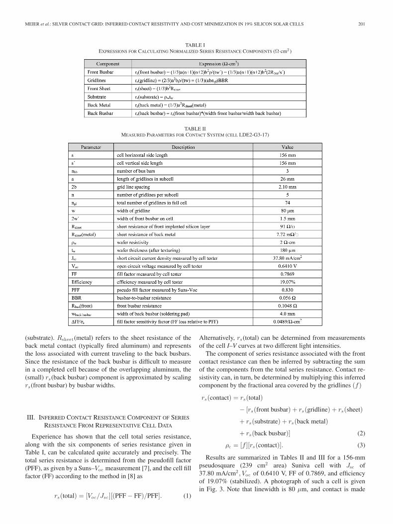
Results are summarized in Tables II and III for a 156-mmpseudosquare (239 cm2 area) Suniva cell with Jsc of37.80 mA/cm2 , Voc of 0.6410 V, FF of 0.7869, and efficiencyof 19.07% (stabilized). A photograph of such a cell is givenin Fig. 3. Note that linewidth is 80 μm, and contact is made
202 IEEE JOURNAL OF PHOTOVOLTAICS, VOL. 3, NO. 1, JANUARY 2013
TABLE IIISERIES RESISTANCE COMPONENTS AND INFERRED CONTACT RESISTIVITY (CELL LDE2-G3-17)
Fig. 3. Photograph of 156-mm pseudosquare cell with grid pattern of the typeanalyzed.
to a 91 Ω/� phosphorus-doped emitter (ion implanted and an-nealed) with a resulting contact resistivity ρc of 5.3 mΩ·cm2 .The phosphorous surface doping concentration is estimated tobe 1.6E20 P/cm3 based on dopant profiles obtained under sim-ilar implant and anneal conditions and measured by the elec-trochemical C–V technique. Since the cell FF was determinedwith a tester having a full metal stage rather than back currentprobes, rs(back metal) and rs (back busbar) do not contribute tothe total series resistance measured, and so are not included inthe calculation of inferred rs(contact). The largest componentsof series resistance are those from the gridlines, front sheet, andfront contact. Overall, shadowing was 6.68% of the cell areaand accounted for a power loss of 1.19 mW/cm2 . Ohmic losseswere 0.95 mW/cm2or 4.98% of the 19.07% cell efficiency.
The value of ρc was also inferred for two other similar cells(efficiency of 19.01% and 19.12%) to be 1.08 and 3.53 mΩ·cm2 ,respectively. The average and standard deviation of ρc for allthree cells is then 3.3 ± 2.1 mΩ·cm2 . Note that (3) is valid pro-vided w/2 < LT , where LT is the current transfer length givenby (
√ρcRsheet) [5]. This requirement is met for the average
contact resistivity (40 μm < 55 μm).
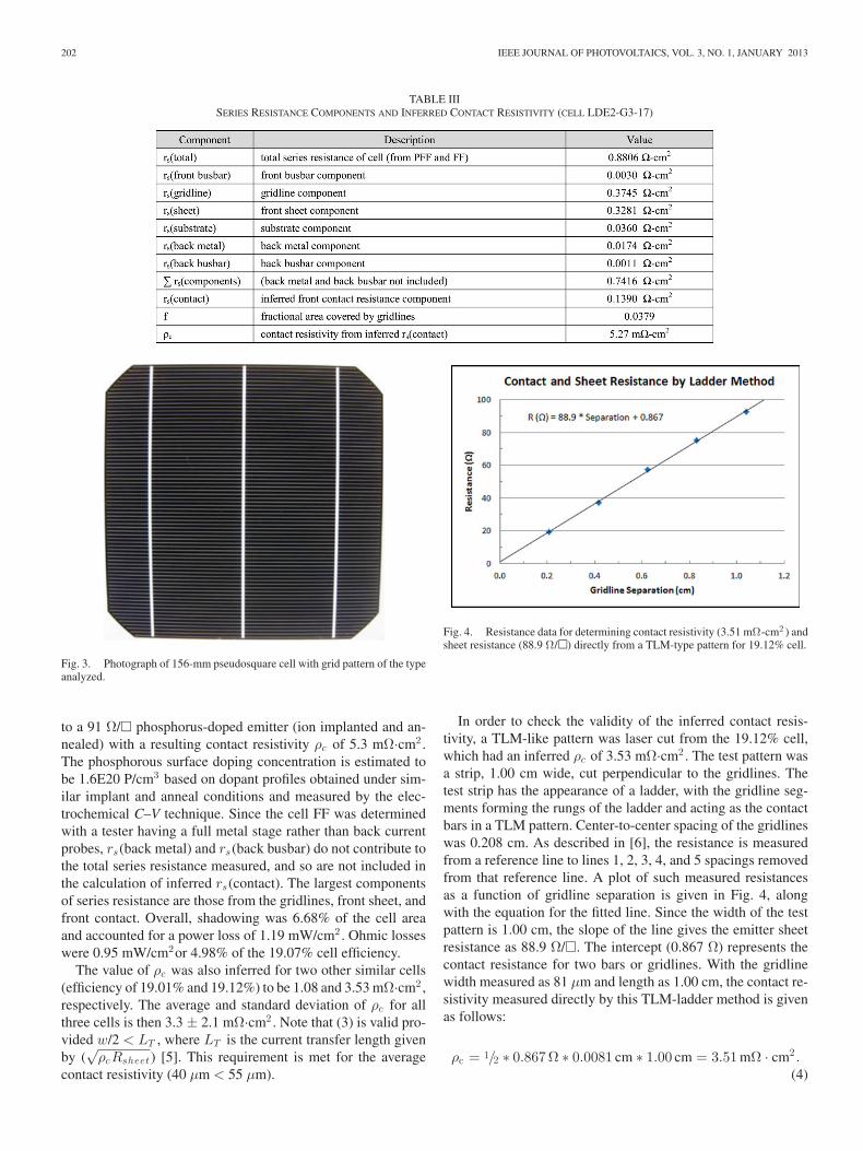
Fig. 4. Resistance data for determining contact resistivity (3.51 mΩ-cm2 ) andsheet resistance (88.9 Ω/�) directly from a TLM-type pattern for 19.12% cell.
In order to check the validity of the inferred contact resis-tivity, a TLM-like pattern was laser cut from the 19.12% cell,which had an inferred ρc of 3.53 mΩ·cm2 . The test pattern wasa strip, 1.00 cm wide, cut perpendicular to the gridlines. Thetest strip has the appearance of a ladder, with the gridline seg-ments forming the rungs of the ladder and acting as the contactbars in a TLM pattern. Center-to-center spacing of the gridlineswas 0.208 cm. As described in [6], the resistance is measuredfrom a reference line to lines 1, 2, 3, 4, and 5 spacings removedfrom that reference line. A plot of such measured resistancesas a function of gridline separation is given in Fig. 4, alongwith the equation for the fitted line. Since the width of the testpattern is 1.00 cm, the slope of the line gives the emitter sheetresistance as 88.9 Ω/�. The intercept (0.867 Ω) represents thecontact resistance for two bars or gridlines. With the gridlinewidth measured as 81 μm and length as 1.00 cm, the contact re-sistivity measured directly by this TLM-ladder method is givenas follows:
ρc = 1/2 ∗ 0.867Ω ∗ 0.0081 cm ∗ 1.00 cm = 3.51 mΩ · cm2 .(4)
MEIER et al.: SILVER CONTACT GRID: INFERRED CONTACT RESISTIVITY AND COST MINIMIZATION IN 19% SILICON SOLAR CELLS 203
This direct measurement of ρc (3.51 mΩ·cm2 ) agrees remark-ably well with the inferred value (3.53 mΩ·cm2 )—in fact, con-siderably better than an error analysis would indicate.
It should be appreciated that the inferred rs (contact) of (2)is small compared with rs (total) in a well-designed cell, and iscalculated based on a number of measured parameters, each ofwhich has an uncertainty (error). An error analysis was carriedout based on standard deviations from five to ten measurementsof the required parameters (except for ρw ), according to [9].The parameters used, along with their standard deviations, are:Voc of 0.6410 ± 0.00012 V, Jsc of 37.80 ± 0.011 mA/cm2 ,FF of 0.7869 ± 0.00126, PFF of 0.830 ± 0.00045, BBR of0.056 ± 0.00142 Ω, Rsheet of 91 ± 3.89 Ω/�, and ρw of2 ± 1 Ω·cm. Equations (1) and (2) then yielded a value ofrs (contact) of 0.139 ± 0.037 Ω·cm2 , or 0.139 Ω·cm2 ± 27%.Contributions to the uncertainty were comparable (within a fac-tor of 3) from the cell parameters of (1), BBR, Rsheet , andρw . Allowing a w value of 80 ± 10 μm to propagate throughf , ρc is determined from (3) to be 5.27 ± 1.55 mΩ·cm2 , or5.27 mΩ·cm2 ± 29%. Thus, the error analysis suggests theinferred contact resistivity is valid to within ± 1.55 mΩ·cm2 .
IV. OPTIMIZING GRIDLINE SPACING FOR MAXIMUM
EFFICIENCY OR FOR MINIMUM COST
With material and geometric contact properties having beenmeasured for a real cell fabricated with current technology, itis now possible to optimize gridline spacing to either maximizeefficiency or minimize incremental cost (Δ$/W) of the frontsilver grid. Recall that measurements from the previous sectionindicated a postfiring silver gridline width of 80 μm. By know-ing the weight of the silver paste used to print the front contact(gridlines and busbars) and the fraction of the paste weight at-tributable to silver (typically 85%), the average thickness ofthe printed silver is calculated to be 7.4 μm. By further know-ing the BBR value, the effective resistivity of the printed silvergridlines is calculated to be 4.7 μΩ·cm (three times the bulkvalue of 1.59 μΩ·cm). The gridline material property (effectiveresistivity) and geometrical properties (width and average thick-ness), which have been demonstrated for current screen-printingtechnology and silver paste composition, remain constant as thespacing between gridlines is varied in an optimization calcu-lation, as does the emitter sheet resistance (91 Ω/�) and theassociated contact resistivity (5.3 mΩ·cm2 ).
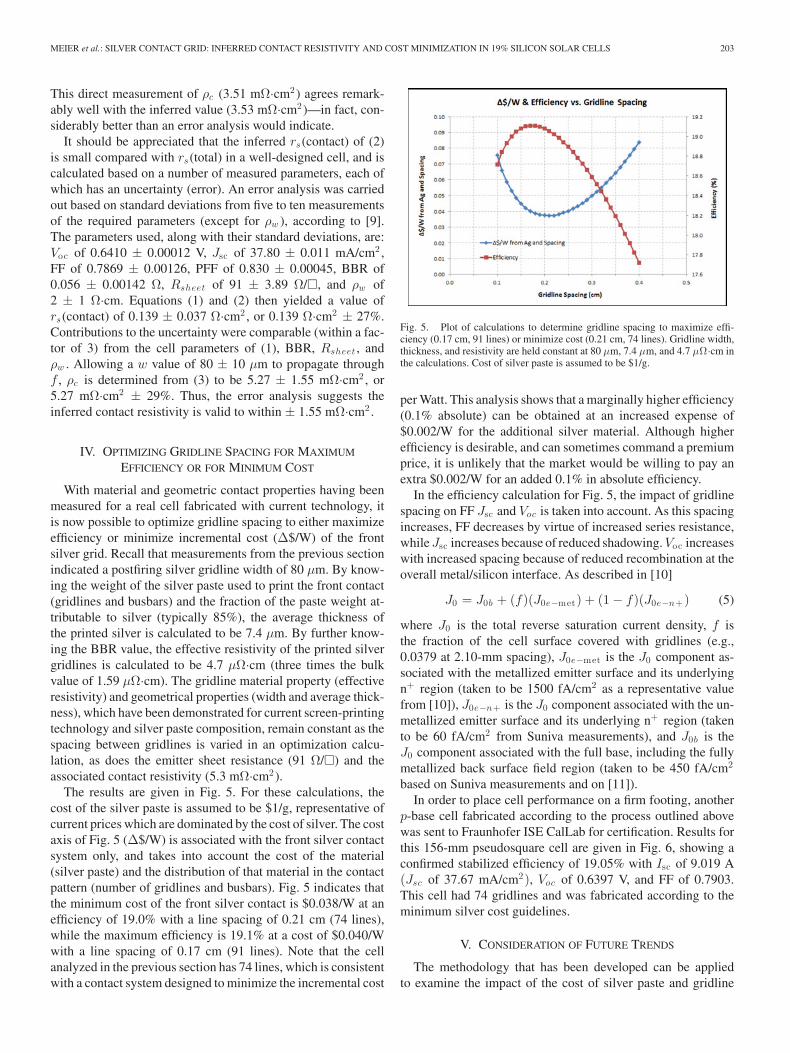
The results are given in Fig. 5. For these calculations, thecost of the silver paste is assumed to be $1/g, representative ofcurrent prices which are dominated by the cost of silver. The costaxis of Fig. 5 (Δ$/W) is associated with the front silver contactsystem only, and takes into account the cost of the material(silver paste) and the distribution of that material in the contactpattern (number of gridlines and busbars). Fig. 5 indicates thatthe minimum cost of the front silver contact is $0.038/W at anefficiency of 19.0% with a line spacing of 0.21 cm (74 lines),while the maximum efficiency is 19.1% at a cost of $0.040/Wwith a line spacing of 0.17 cm (91 lines). Note that the cellanalyzed in the previous section has 74 lines, which is consistentwith a contact system designed to minimize the incremental cost
Fig. 5. Plot of calculations to determine gridline spacing to maximize effi-ciency (0.17 cm, 91 lines) or minimize cost (0.21 cm, 74 lines). Gridline width,thickness, and resistivity are held constant at 80 μm, 7.4 μm, and 4.7 μΩ·cm inthe calculations. Cost of silver paste is assumed to be $1/g.
per Watt. This analysis shows that a marginally higher efficiency(0.1% absolute) can be obtained at an increased expense of$0.002/W for the additional silver material. Although higherefficiency is desirable, and can sometimes command a premiumprice, it is unlikely that the market would be willing to pay anextra $0.002/W for an added 0.1% in absolute efficiency.
In the efficiency calculation for Fig. 5, the impact of gridlinespacing on FF Jsc and Voc is taken into account. As this spacingincreases, FF decreases by virtue of increased series resistance,while Jsc increases because of reduced shadowing. Voc increaseswith increased spacing because of reduced recombination at theoverall metal/silicon interface. As described in [10]
J0 = J0b + (f)(J0e−met) + (1 − f)(J0e−n+) (5)
where J0 is the total reverse saturation current density, f isthe fraction of the cell surface covered with gridlines (e.g.,0.0379 at 2.10-mm spacing), J0e−met is the J0 component as-sociated with the metallized emitter surface and its underlyingn+ region (taken to be 1500 fA/cm2 as a representative valuefrom [10]), J0e−n+ is the J0 component associated with the un-metallized emitter surface and its underlying n+ region (takento be 60 fA/cm2 from Suniva measurements), and J0b is theJ0 component associated with the full base, including the fullymetallized back surface field region (taken to be 450 fA/cm2
based on Suniva measurements and on [11]).In order to place cell performance on a firm footing, another
p-base cell fabricated according to the process outlined abovewas sent to Fraunhofer ISE CalLab for certification. Results forthis 156-mm pseudosquare cell are given in Fig. 6, showing aconfirmed stabilized efficiency of 19.05% with Isc of 9.019 A(Jsc of 37.67 mA/cm2), Voc of 0.6397 V, and FF of 0.7903.This cell had 74 gridlines and was fabricated according to theminimum silver cost guidelines.
V. CONSIDERATION OF FUTURE TRENDS
The methodology that has been developed can be appliedto examine the impact of the cost of silver paste and gridline

204 IEEE JOURNAL OF PHOTOVOLTAICS, VOL. 3, NO. 1, JANUARY 2013
Fig. 6. Fraunhofer-certified 19.05% cell (Suniva cell SUN_SEL_8).
Fig. 7. Calculated cell efficiency resulting from optimizing gridline spacing toeither maximize efficiency or minimize silver cost, with silver cost and gridlinewidth as parameters. (Troy Ounce is abbreviated as oz.)
Fig. 8. Calculated gridline spacing to either maximize efficiency or minimizesilver cost with silver cost and gridline width as parameters. (Troy Ounce isabbreviated as oz.)
width on cell efficiency and on gridline spacing. Figs. 7 and8 summarize the results of one such analysis. In all cases, thevalues of average gridline thickness (7.4 μm), gridline width(80 μm), effective gridline resistivity (4.7 μΩ·cm), contact re-sistivity (5.3 mΩ·cm2 ), and emitter sheet resistance (91 Ω/�)
that were extracted from measurements and analysis of a fab-ricated cell were used. In Figs. 7 and 8, Troy Ounce is abbre-viated as oz, where 1 oz is equivalent to 31.1 g. Note that assilver prices go up, efficiency decreases (see Fig. 7) and gridlinespacing increases (see Fig. 8) in order to minimize Δ$/W. Max-imum efficiency is independent of silver cost and favors narrowgridlines with small spacing, as expected.
VI. CONCLUSION
From this paper, the following conclusions can be drawn.1) Accurate analysis of the gridline loss component in an
H-bar contact grid system is greatly facilitated by a simplemeasurement of busbar-to-busbar resistance.
2) The proper treatment of current arriving at a busbar fromdiscrete gridlines gives a series resistance component forthe busbar, which is a factor of [(n + 1)(n + 2)]/n2 largerthan that given assuming a continuous flow of current intothe busbar, where n is the number of gridlines per currentprobe.
3) Contact resistivity of the front silver contact can be in-ferred from the measurement of pseudo FF (Suns–Voc),cell Jsc , Voc , and FF (I–V curve) and the determination ofsix components of series resistance along with the frac-tional area covered—without resorting to a TLM measure-ment.
4) Error analysis suggests inferred contact resistivity is ac-curate to within approximately ± 1.6 mΩ·cm2 .
5) Current screen-printing technology and silver paste al-low for a contact resistivity of approximately 3.3 mΩ·cm2
when contacting a 90 Ω/� ion implanted/annealedphosphorus-doped emitter.
6) Current screen-printing technology and silver paste costindicate gridline spacing of 1.7 mm to maximize efficiencyand 2.1 mm to minimize silver cost.
7) Guidance regarding optimum gridline spacing (screen de-sign), which follows from future silver price changes orlifting of technological limits (gridline width) is availablethrough a contact analysis, as described.
8) Contact analysis helps to enable full-sized (239 cm2)production-worthy cells fabricated from p-Cz silicon sub-strates with efficiencies in excess of 19%, as confirmed byFraunhofer ISE CalLab.
ACKNOWLEDGMENT
The authors gratefully acknowledge the Suniva productionstaff and the Suniva R&D staff for their assistance in processingthe cells used in this study.
REFERENCES
[1] M. Wolf, “Metallization for large-area solar cells,” in Proc. 15th Photo-voltaic Spec. Conf., 1981, pp. 506–511.
[2] L. J. Caballero, P. Sanchez-Friera, B. Lalajuna, J. Alonso, andM. A. Vazquez, “Series resistance modeling of industrial screen-printedmonocrystalline silicon solar cells and modules including the effect ofspot soldering,” in Proc. 4th World Conf. Photovoltaic Energy Convers.,2006, pp. 1388–1391.
MEIER et al.: SILVER CONTACT GRID: INFERRED CONTACT RESISTIVITY AND COST MINIMIZATION IN 19% SILICON SOLAR CELLS 205
[3] L. J. Caballero, A. Martinez, P. Sanchez-Friera, M. A. Vazquez, andJ. Alonso, “Front grid design in industrial silicon solar cells: Modelling toevaluate the behaviour of three vs. two buses cell patterns,” in Proc. 33rdPhotovoltaic Spec. Conf., 2008, pp. 1–4.
[4] L. J. Caballero, “Contact definition in industrial silicon solar cells,” inSolar Energy, Rijeka, Croatia: Intech, 2010, ch. 16, pp. 375–398.
[5] D. L. Meier and D. K. Schroder, “Contact resistance: Its measurement andrelative importance to power loss in a solar cell,” IEEE Trans. ElectronDevices, vol. 31, no. 5, pp. 647–653, May 1984.
[6] D. L. Meier, E. A. Good, R. A. Garcia, B. B. Bingham, S. Yamanaka,V. Chandrasekaran, and C. Bucher, “Determining components of seriesresistance from measurements on a finished cell,” in Proc. 4th World Conf.Photovoltaic Energy Convers., May 2006, pp. 1315–1318.
[7] R. A. Sinton, A. Cuevas, and M. Stuckings, “Quasi-steady-state photo-conductance: A new method for solar cell material and device characteri-zation,” in Proc. 25th Photovoltaic Spec. Conf., May 1996, pp. 457–460.
[8] A. L. Fahrenbruch and R. H. Bube, Fundamentals of Solar Cells, NewYork: Academic, 1983, pp. 220–222.
[9] P. R. Bevington, Data Reduction and Error Analysis for the PhysicalSciences, New York: McGraw-Hill, 1969, pp. 56–65.
[10] T. Fellmeth, A. Born, A. Kimmerle, F. Clement, D. Biro, and R. Preu,“Recombination at metal emitter interfaces of front contact technologiesfor highly efficient silicon solar cells,” Energy Procedia, vol. 8, pp. 115–121, 2011.
[11] R. Woehl, P. Gundel, J. Krause, K. Ruhle, F. D. Heinz, M. Rauer,C. Schmiga, M. C. Schubert, W. Warta, and D. Biro, “Evaluating thealuminum-alloyed p+ -layer of silicon solar cells by emitter saturation cur-rent density and optical microspectroscopy measurements,” IEEE Trans.Electron Devices, vol. 58, no. 2, pp. 441–447, Feb. 2011.
Daniel L. Meier (M’08) received the B.S. degreein physics from St. Vincent College, Latrobe, PA, in1969 and the M.S. degrees in physics in 1971 andin measurement and control in 1978, and the Ph.D.degree in solid state physics in 1976, from Carnegie-Mellon University (CMU), Pittsburgh, PA.
After spending four years in the field of ocean ther-mal energy conversion at CMU, he began his careerin photovoltaics in 1980 with the Westinghouse Elec-tric Corporation. Over the years, he has held a varietyof scientific and executive positions with Westing-
house, EBARA Solar, Solar Power Industries, the National Renewable EnergyLaboratory, and Suniva, Norcross, GA – most recently as Chief Scientist withSuniva. After leaving Suniva in 2012, he founded Lightdrop Harvest, LLC, St.Marys, PA, to offer consulting services to the photovoltaics community. Hehas published over 90 technical papers and has been granted 13 U.S. patents.His research interests include the design, fabrication, and characterization ofproduction-worthy silicon solar cells and modules, with emphasis on junctionformation by ion implantation and on contact systems.
Vinodh Chandrasekaran (M’12) received the B.E. degree in electronics andcommunication engineering from the University of Madras, Chennai, India, in2002 and the M.S.E.E. degree from the University of South Florida, Tampa,specializing in thin-film photovoltaics, in 2005.
He is currently a Senior R&D Engineer with Suniva, Norcross, GA, where heis primarily responsible for development of contacts to advanced cell structuresand cost reduction. He has also been focused on the development and transferof technology from the lab, achieving cell efficiency levels of more than 19% inproduction. Prior to joining Suniva, he was with Solar Power Industries, wherehe worked on the development and manufacturing of multicrystalline siliconsolar cells. He was also involved in multicrystalline ingot growth and the wiresawing process.
Atul Gupta received the B.S. degree in chemicalengineering from the Indian Institute of Technol-ogy, Delhi, in 1996, two M.S. degrees in chemicaland electrical and computer engineering in 1999 and2000, respectively, and the Ph.D. degree in chemicalengineering in 2001, all from from North CarolinaState University, Raleigh.
He has been with Suniva, Norcross, GA, since2011, where he is currently the Director of ProductDevelopment and R&D. He has several papers in thisfield and has been awarded 20 patents. He has held
several positions of increasing responsibility since 2001, starting his industrycareer at the R&D headquarters of Advanced Micro Devices, where his primaryresponsibility was developing and transferring new processes and technologiesin thin-film deposition for complementary metal-oxide semiconductor device(logic and flash memory) manufacturing. He then joined Varian SemiconductorEquipment as principal engineer, where he was responsible first for developinga plasma doping implanter and then was instrumental in creating a new busi-ness unit focused on developing an implanter for solar cell manufacturing. Hisprimary responsibilities include the development and deployment of new cellstructures that meet industry leading high-efficiency and lower cost objectivesfor Suniva, in addition to managing the intellectual property portfolio for Suniva.
Vijay Yelundur received the B.S. and the Ph.D. degrees in materials science andengineering from the Georgia Institute of Technology (Georgia Tech), Atlanta,in 1997 and 2003, respectively.
He is currently Manager of the Manufacturing Innovation Center, Suniva,Norcross, GA, where he is involved with low-cost c-Si cell technology devel-opment and transfer into manufacturing. He joined Suniva after five years as aSenior Research Engineer with the University Center of Excellence for Photo-voltaics Research and Education at Georgia Tech, where his research interestsincluded process integration for high-efficiency manufacturable c-Si solar cellsand the gettering and passivation of defects in low-cost Si materials. He haspublished more than 30 technical papers in the field of c-Si photovoltaics.
Ajeet Rohatgi (F’08) received the B.S. degree inelectrical engineering from the Indian Institute ofTechnology, Kanpur, India, in 1971, the M.S. de-gree from Virginia Tech, Blacksburg, in 1973, andthe Ph.D. degree in metallurgy and material sciencefrom Lehigh University, Bethlehem, PA, in 1977.
He is currently a Regents’ Professor and a Geor-gia Power Distinguished Professor with the Schoolof Electrical Engineering, Georgia Institute of Tech-nology (Georgia Tech), Atlanta. In 2007, he foundedSuniva, Inc., Norcross, GA, to manufacture silicon
solar cells and modules that are situated at the right intersection of cost andefficiency, where he is the Chief Technology Ofiicer. He is the also the foundingdirector of the University Center of Excellence for Photovoltaic Research andEducation, Georgia Tech. He has published more than 400 technical papers inthis field and has been awarded 15 patents. As part of the 1996 Olympics in At-lanta, he and his group designed and installed the world’s largest grid-connected,roof-top photovoltaic (PV) system on the Georgia Tech Aquatic Center. His cur-rent research interests include the development of cost and efficiency roadmapsfor attaining grid parity with Silicon PV, understanding of impurity effects insilicon solar cells, gettering and passivation of defects in solar grade silicon, ionimplantation and rapid thermal processing of solar cells, the design and fabrica-tion of high-efficiency commercial ready n- and p-base silicon solar cells, andthe economics of PV systems.
Dr. Rohatgi received the Westinghouse Engineering Achievement Award in1985, the Distinguished Professor Award from Georgia Tech in 1996, the IEEEPVSC William Cherry Award in 2003, the Climate Protection Award from theEnvironmental Protection Agency, and the Outstanding Educator and InnovatorAward in PV from the American Solar Energy Society in 2009. In 2010, he wasnamed one of the Champions of PV by Renewable Energy World magazine.