ht46 a/d type mcu series data memory (byte) program memory ht46r22 (otp) ht46c22 (mask) 2kx14 64...
Post on 21-Dec-2015
223 views
TRANSCRIPT
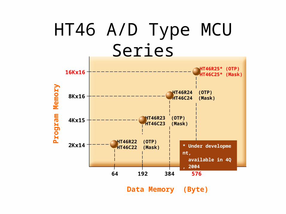
HT46 A/D Type MCU Series
Data Memory (Byte)
Pro
gra
m M
emo
ry
HT46R22 (OTP)HT46C22 (Mask)2Kx14
64
8Kx16
4Kx15
192 384
HT46R23 (OTP)HT46C23 (Mask)
HT46R24 (OTP)HT46C24 (Mask)
HT46R25* (OTP)HT46C25* (Mask)16Kx16
576
* Under development,
available in 4Q, 2004
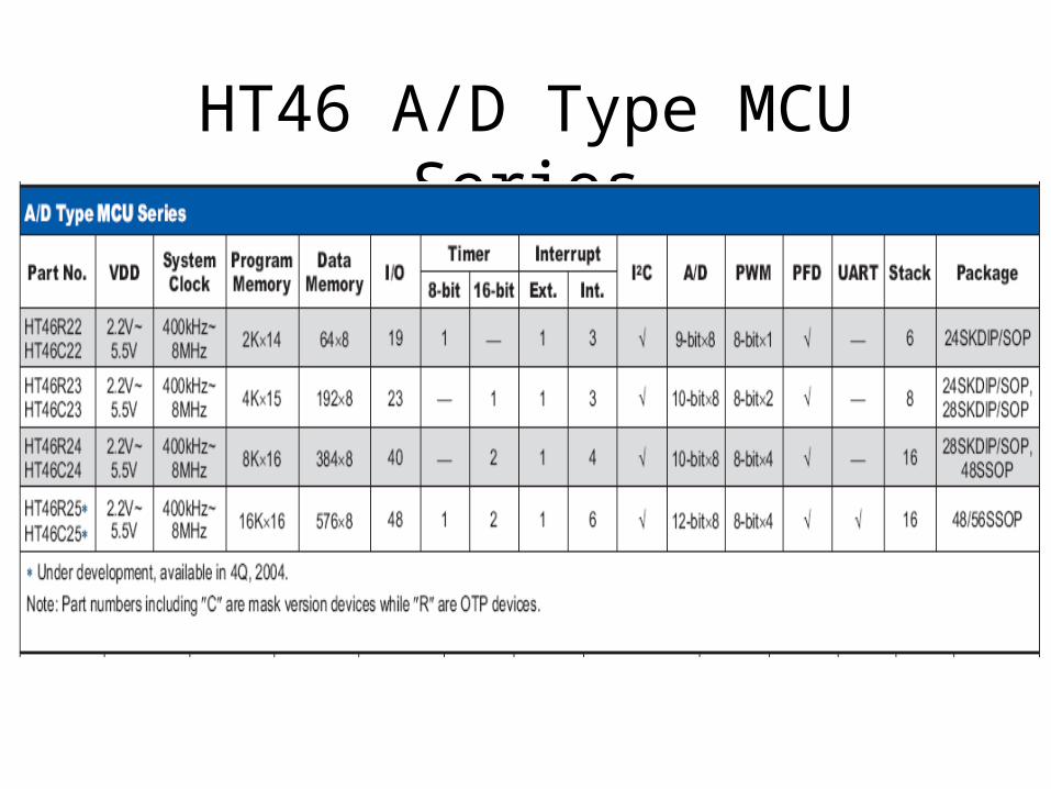
HT46 A/D Type MCU Series
Features of A/D Type HT46 Series
• RISC Architecture• Direct and Indirect
Addressing mode.• Total 63 instructions.• Table read function.• Maximum 16 stack ( by
product)
• Operating Voltage:– Fsys = 4Mhz, 2.2~5.5v– Fsys = 8Mhz, 3.3~5.5v
• Idd : 2mA (tpy.) (5V, 4MHz, Xtal, ADC disable)
• Istb : 1uA (max.) (WDT, RTC disabled).
• -40oC~85oC Operating temperature.(Industrial grade)
Peripheral Feature
• I/O with pull high function.
• Port A with wake up function.
• Timer function• Watch dog function• Halt and wakeup for
low power consumption.• I2C interface
• PFD driver output.• On-chip crystal and RC
oscillator• LVR for Brown-out
protection.• Multi-channel 9 or 10-bit
A/D converter• Pulse Width Modulator
output.
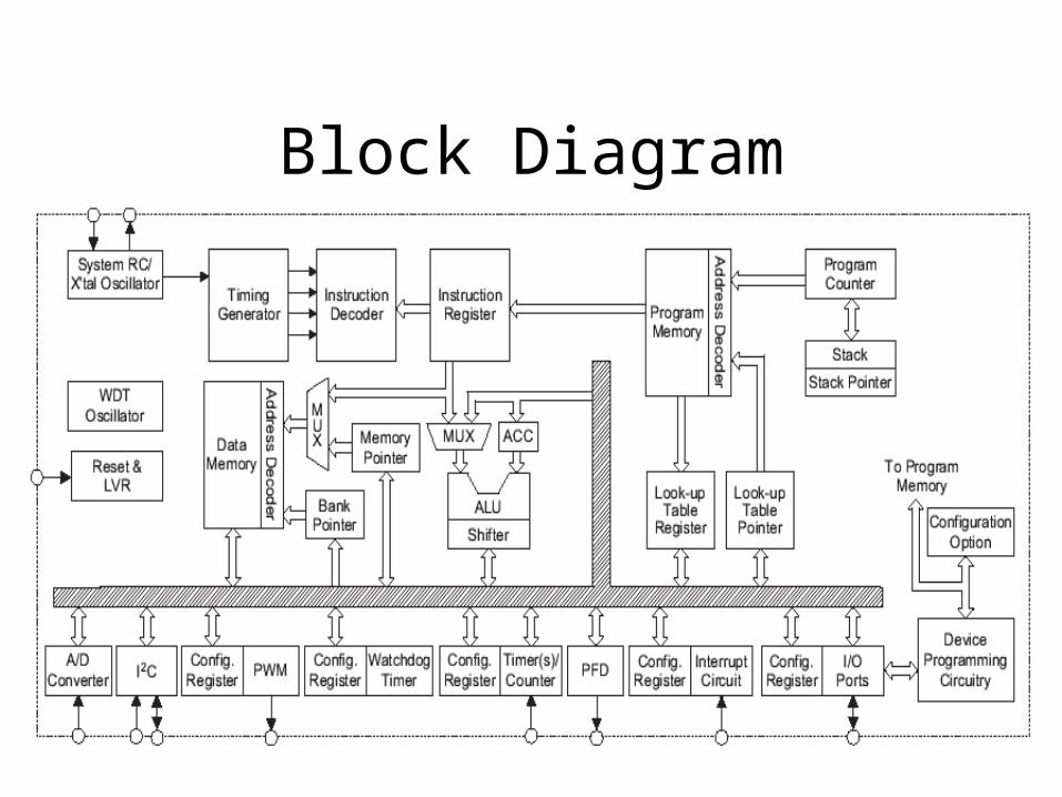
Block Diagram
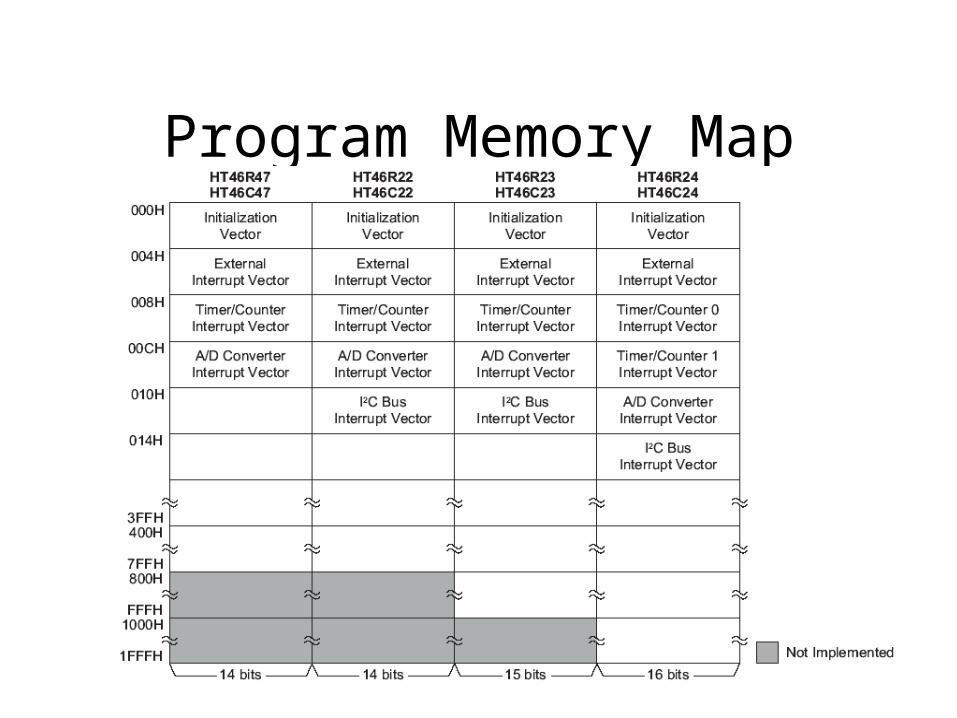
Program Memory Map

Special Purpose Data Memory
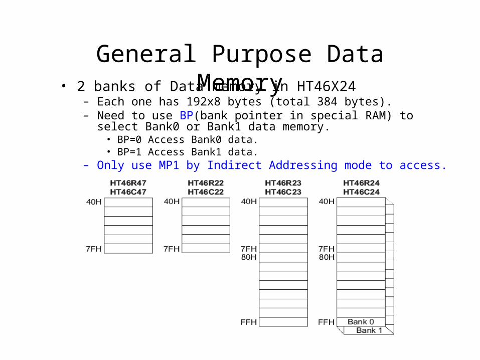
General Purpose Data Memory• 2 banks of Data memory in HT46X24
– Each one has 192x8 bytes (total 384 bytes).– Need to use BP(bank pointer in special RAM) to select Bank0 or Bank1
data memory.• BP=0 Access Bank0 data.• BP=1 Access Bank1 data.
– Only use MP1 by Indirect Addressing mode to access.
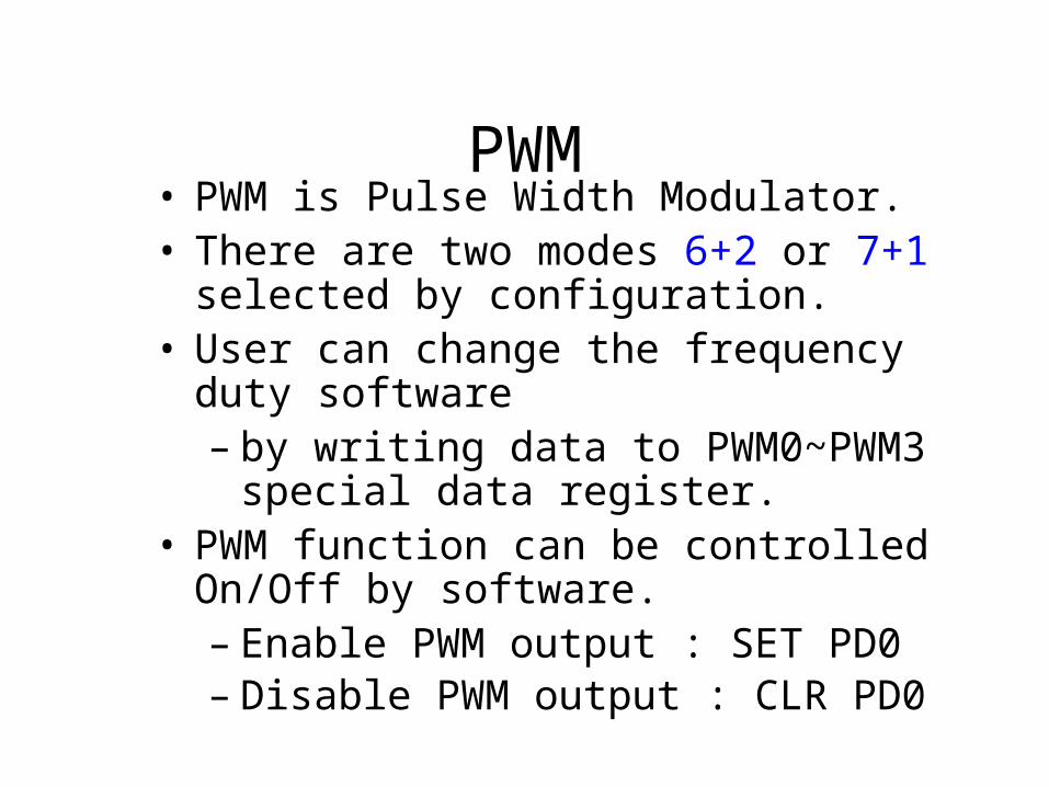
PWM• PWM is Pulse Width Modulator. • There are two modes 6+2 or 7+1 selected by
configuration.• User can change the frequency duty software
– by writing data to PWM0~PWM3 special data register.
• PWM function can be controlled On/Off by software.– Enable PWM output : SET PD0– Disable PWM output : CLR PD0

PWM 6+2 Mode
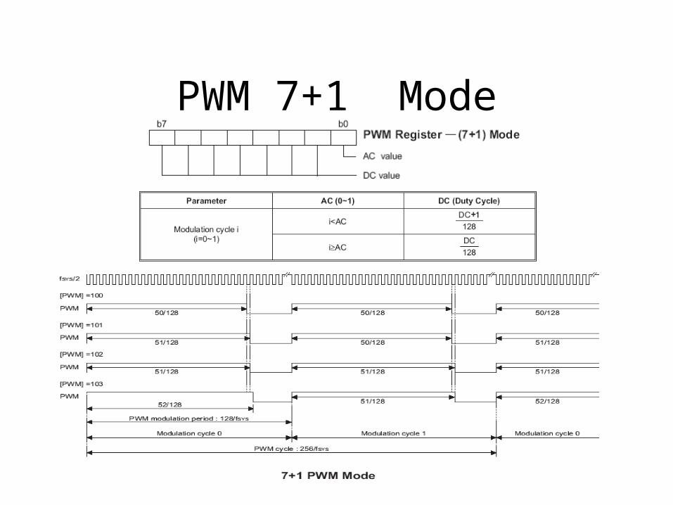
PWM 7+1 Mode

Analog to Digital Converter• The HT46 series have a 9 or 10-bit ADC. • ADC can be disabled by software.• Max. 4 or 8 channels can input to the ADC.
– Channels set in ADCR by software• ADC channels are pin-shared with Port B.
– As ADC input or Port B set in ADCR by software• Input range is from 0 to VDD.• Min. ADC clock period is 1us.• ADC sampling time is 32 ADC clocks.• ADC convert time is 76 ADC clocks.• Max. INL ± 1 LSB.
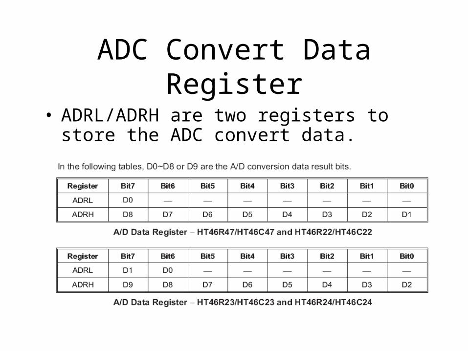
ADC Convert Data Register
• ADRL/ADRH are two registers to store the ADC convert data.
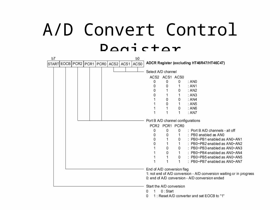
A/D Convert Control Register
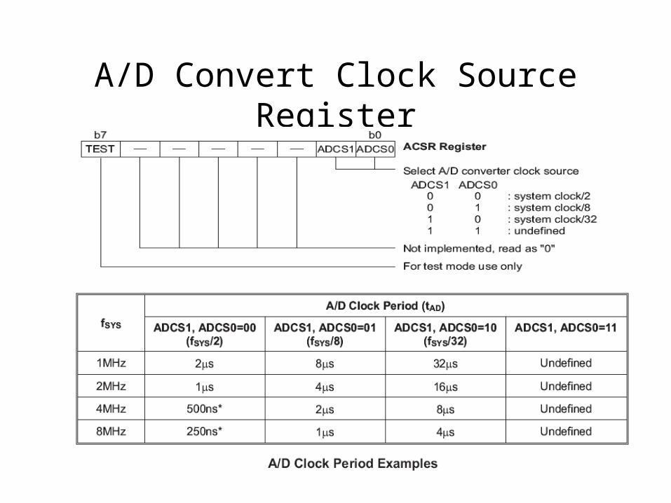
A/D Convert Clock Source Register
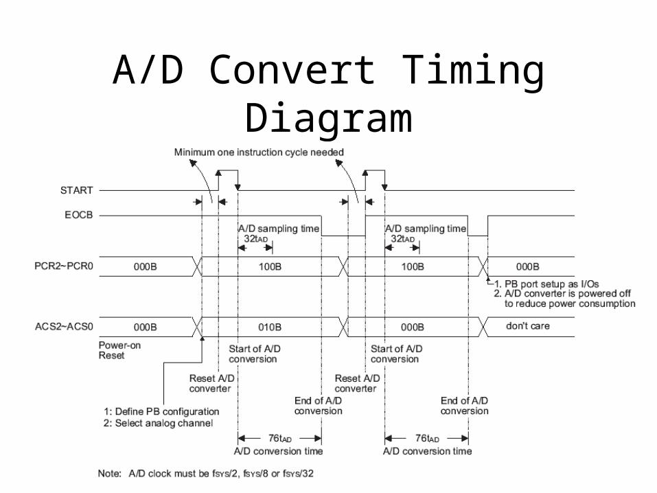
A/D Convert Timing Diagram
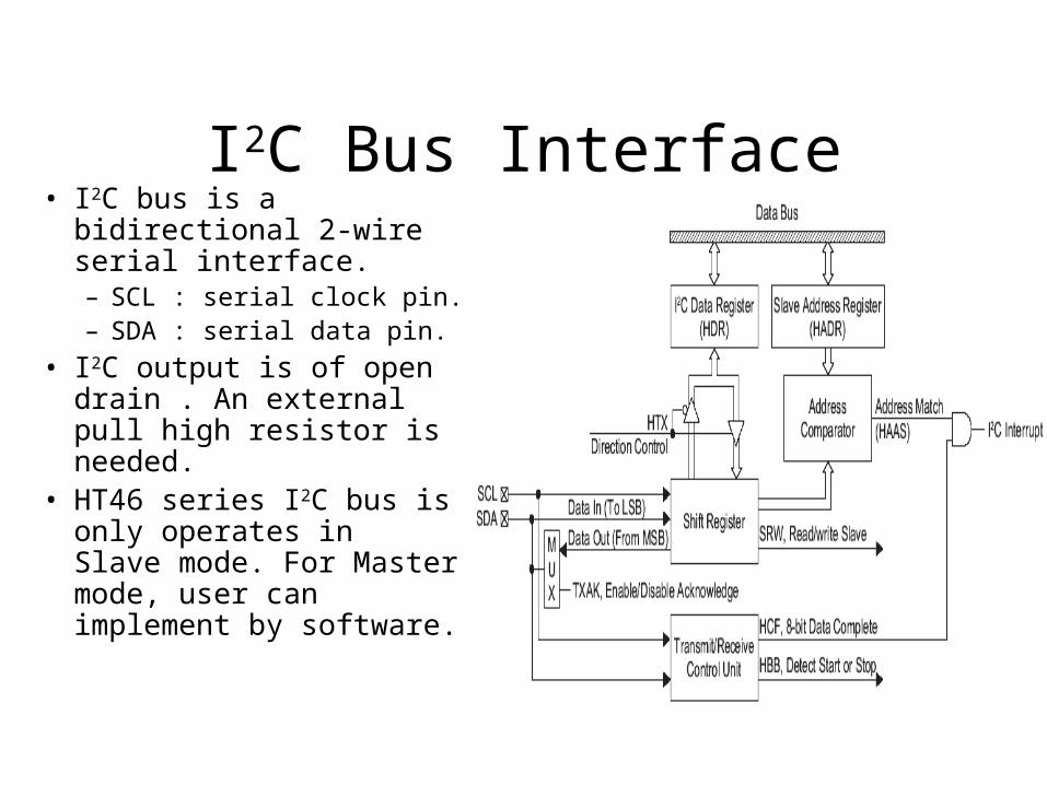
I2C Bus Interface• I2C bus is a bidirectional
2-wire serial interface.– SCL : serial clock pin.– SDA : serial data pin.
• I2C output is of open drain . An external pull high resistor is needed.
• HT46 series I2C bus is only operates in Slave mode. For Master mode, user can implement by software.

I2C Registers• I2C Slave Address
Register - HADR• I2C Input/Output Data
Register – HDR• I2C Control Register –
HCR.• I2C Status Register –
HRS.• Using HT46 serial I2C
Slave function, user can only need to set some flags and polling some status flags. Then, I2C bus can work.
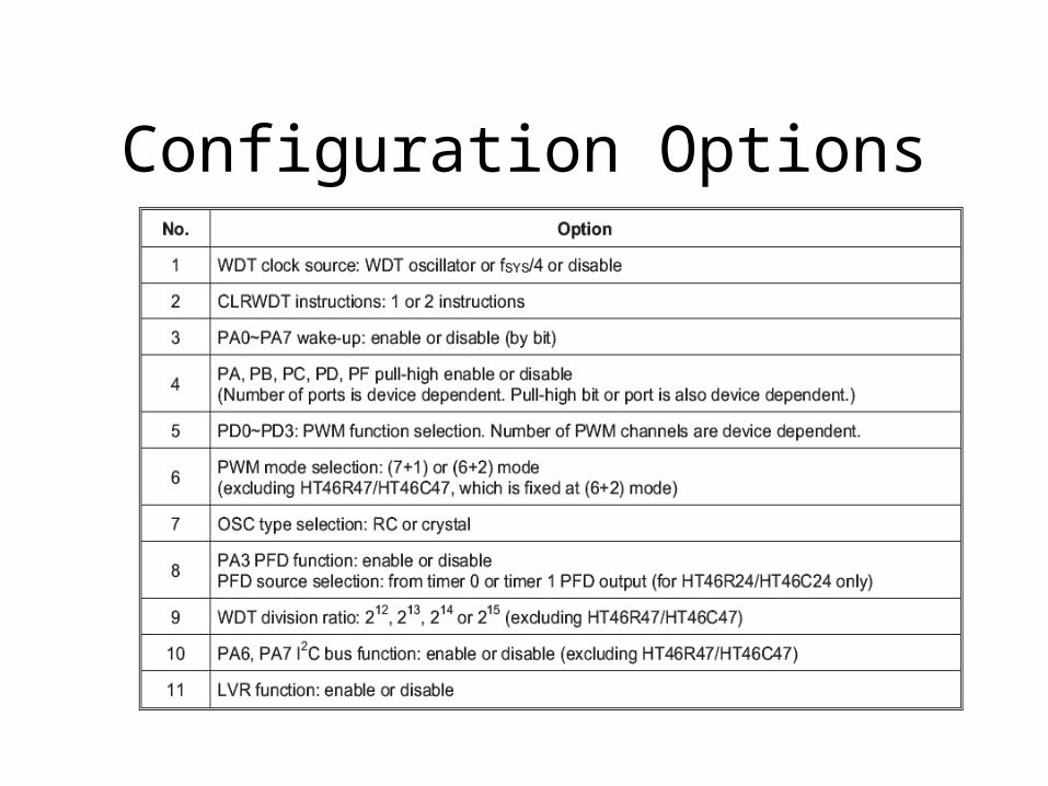
Configuration Options