how to design power electronics - keysight · pdf filehow to design power electronics the hf...
TRANSCRIPT

How to Design Power Electronics
The HF in Power Semiconductor Modeling and Design
Innovations in EDA Webcast Series
September 3, 2015
Ingmar Kallfass
Institute of Robust Power Semiconductor Systems
University of Stuttgart

Outline
• Semiconductor-Based Power Electronics
• An Introduction
• Challenges in Power Module Design
• Power Module Design Flow
• Modeling and Characterization
• Electro-Thermal Co-Simulation
• GaN Integration: Power Electronic
Circuits
2
03/09/15
Innovations in EDA Webcast Series
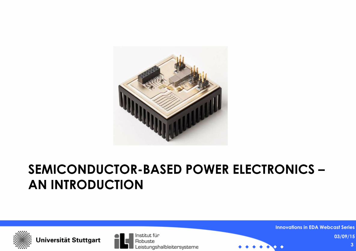
SEMICONDUCTOR-BASED POWER ELECTRONICS –
AN INTRODUCTION
3
03/09/15
Innovations in EDA Webcast Series

Where Power Electronics meet Microwaves Semiconductor Technologies
4
Frequency
Po
we
r
Scaling & Device Engineering
Performance
Maturity & Reliability
Cost
Share of Markets and Applications
Silicon IGBT
MOSFET
vs.
Compounds SiC
MOSFET/IGBT
GaN HEMT
Compounds GaAs/InP
HEMT/HBT
GaN HEMT
vs.
Silicon
MOSFET
SiGe HBT
Innovations in EDA Webcast Series
03/09/15

Power Electronics – A Definition
„Power Electronics is the extension of solid-state electronics away from
handling communications and data and into the business of efficiently
handling power, from milliwatts to gigawatts.
It makes the mobile phone battery last longer, it makes hybrid cars
practicable, and it helps make electrical generation and distribution
possible from sources ranging from a solar cell on your roof to a nuclear
reactor in mainland Europe.”
[BIS]
5
03/09/15
Innovations in EDA Webcast Series
Power Electronics – A Definition
„Power Electronics is (...) an enabling technology that often determines the
performance of, and provides the competitive advantage for, much more
expensive devices or systems. For example, choosing a mobile phone or
lap-top computer for its battery life is actually a Power Electronics decision,
with the battery performance itself just one part of that.
The importance of Power Electronics to the economy is consequently very
much greater than its direct market value.
Power Electronics is rarely seen as an end product by the general public,
but it does play a critical role in almost all aspects of our daily lives.”
[BIS]
6
03/09/15
Innovations in EDA Webcast Series

Applications and Technologies
7
03/09/15
Innovations in EDA Webcast Series
Source: „GaN-on-Si power transistors from French lab Leti”, CEA-Leti
http://www.electronicsweekly.com/news/design/power/gan-on-si-power-transistors-french-lab-leti-2015-07/

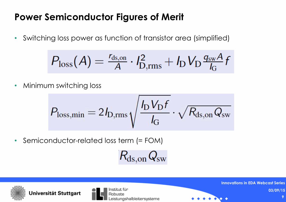
Power Semiconductor Figures of Merit
• Johnson FOM
• describes the capability of power handling at
high frequencies
• Baliga FOM
• describes the capability of minimizing on-state power loss in a transistor switch, i.e. loss due to
current flow through on-resistance
8
03/09/15
Innovations in EDA Webcast Series
Power Semiconductor Figures of Merit
• Switching loss power as function of transistor area (simplified)
• Minimum switching loss
• Semiconductor-related loss term (= FOM)
9
03/09/15
Innovations in EDA Webcast Series

FOM Power Semiconductors
10
03/09/15
Innovations in EDA Webcast Series
[Catrene]

SEMICONDUCTOR-BASED POWER ELECTRONICS –
CHALLENGES IN POWER MODULE DESIGN
11
03/09/15
Innovations in EDA Webcast Series

Power Conversion:
Small and Light, but also Efficient, Robust and EM Compatible
12
03/09/15
Innovations in EDA Webcast Series
power density [W/cm3]
effic
ien
cy [%
]

ECPE* Technology Roadmap
Requirement Key Performance
Indicator
Goal: Improvement by
2020 by a factor of
size power density
[kW/l]
2-3
weight power-to-mass ratio
[kW/kg]
2
efficiency efficiency
[%]
3
cost relative cost
[kW/€]
2-3
robustness failure rate
[1/h]
3
13
03/09/15
Innovations in EDA Webcast Series
65 W
[golem.de]
60 W
DC-DC PSiP
24 W/cm3
*European Center for Power Electronics

Design Measures in Switched-Mode Converters
14
03/09/15
Innovations in EDA Webcast Series
Control Filters (Passives)
Transistor Power Switches
Reduction of Related entities Measures
Size, weight of passives
high fsw
Transistor switching loss small FOM = RonQsw
high d/dt slopes
Parasitic LC resonance
(gate and power loops)
compact layout & high
integration density
Cooling effort high temp. operation
of wide-bandgap SC
EMC shielding/filtering EMC-oriented design

Tradeoffs
fsw d/dt high T operation integration
density
size
weight
efficiency
cost
robustness
EMC
15
03/09/15
Innovations in EDA Webcast Series
Optimum design requires an RF-refined design flow
from device characterization and modeling
to multi-domain circuit analysis

Multi-Domain Modeling & Design
16
Innovations in EDA Webcast Series
03/09/15
Modeling
Transistor
Package
DBC, PCB
static
dynamic
thermal
Rth
,HS
Cth,J
Rth
,JC
Cth,HS
Characterization Modeling Design
IV
CV
QV
vs Temperature
LF dispersion
Thermal impedance
B1506A
electro-thermal
co-simulation
electro-magnetic
simulation
time and
frequency domain
analysis
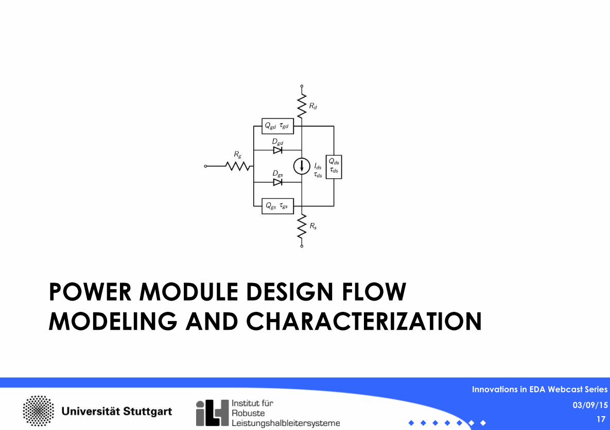
POWER MODULE DESIGN FLOW
MODELING AND CHARACTERIZATION
17
03/09/15
Innovations in EDA Webcast Series
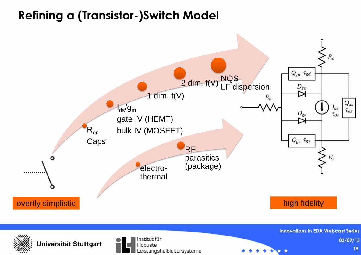
Refining a (Transistor-)Switch Model
18
03/09/15
Innovations in EDA Webcast Series
Ron
Caps
Ids/gm
gate IV (HEMT)
bulk IV (MOSFET)
1 dim. f(V)
2 dim. f(V) NQS LF dispersion
electro-thermal
RF parasitics (package)
high fidelity overtly simplistic

Dynamic IV for Switching of Inductive Loads
19
03/09/15
Innovations in EDA Webcast Series
1
2 3
Id
Vds
VDS ID
VG
tON tcross OFF
t
t
VG
Vin IdMAX
PLOSS
tcross ON
VPlateau
1 2 3
Gate charge is required for the
calculation of switching loss
and efficiency

Dynamic IV for Switching of Inductive Loads
20
03/09/15
Innovations in EDA Webcast Series
Dynamic IV in a FET transistor switch transits from sub-threshold to saturation to linear regime
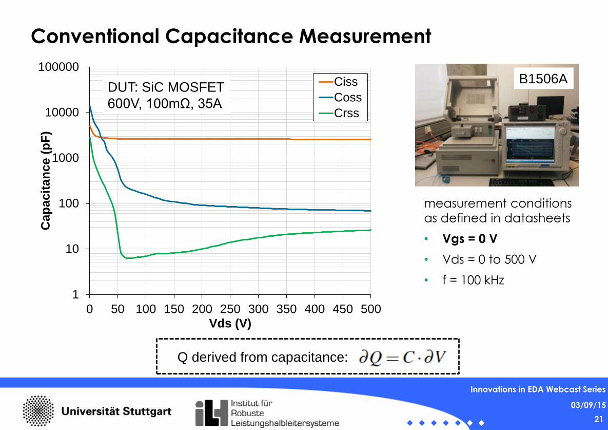
Conventional Capacitance Measurement
21
03/09/15
Innovations in EDA Webcast Series
1
10
100
1000
10000
100000
0 50 100 150 200 250 300 350 400 450 500
Cap
acit
an
ce (
pF
)
Vds (V)
Ciss
Coss
Crss
measurement conditions
as defined in datasheets
• Vgs = 0 V
• Vds = 0 to 500 V
• f = 100 kHz
DUT: SiC MOSFET
600V, 100mΩ, 35A
B1506A
Q derived from capacitance:
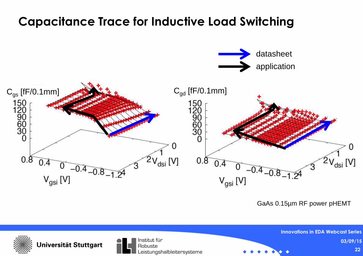
Capacitance Trace for Inductive Load Switching
22
03/09/15
Innovations in EDA Webcast Series
GaAs 0.15µm RF power pHEMT
Cgs [fF/0.1mm] Cgd [fF/0.1mm]
datasheet
application
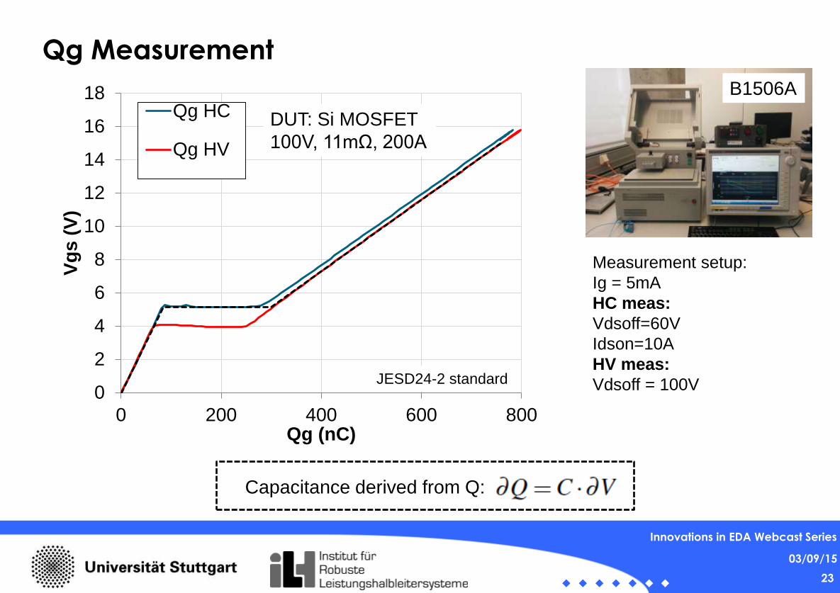
Qg Measurement
23
03/09/15
Innovations in EDA Webcast Series
0
2
4
6
8
10
12
14
16
18
0 200 400 600 800
Vg
s (
V)
Qg (nC)
Qg HC
Qg HV
Measurement setup:
Ig = 5mA
HC meas:
Vdsoff=60V
Idson=10A
HV meas:
Vdsoff = 100V
DUT: Si MOSFET
100V, 11mΩ, 200A
B1506A
Capacitance derived from Q:
JESD24-2 standard

Traps in GaN Devices
• well known from RF devices
• „drain-lag“/“gate-lag“
• LF dispersion
• dynamic Ron
• after OFF-to-ON switching,
Ron remains high for a period
of time
• trapping time constants from
ns to ms or even longer (continuous exposure)
24
03/09/15
Innovations in EDA Webcast Series
[Catrene]
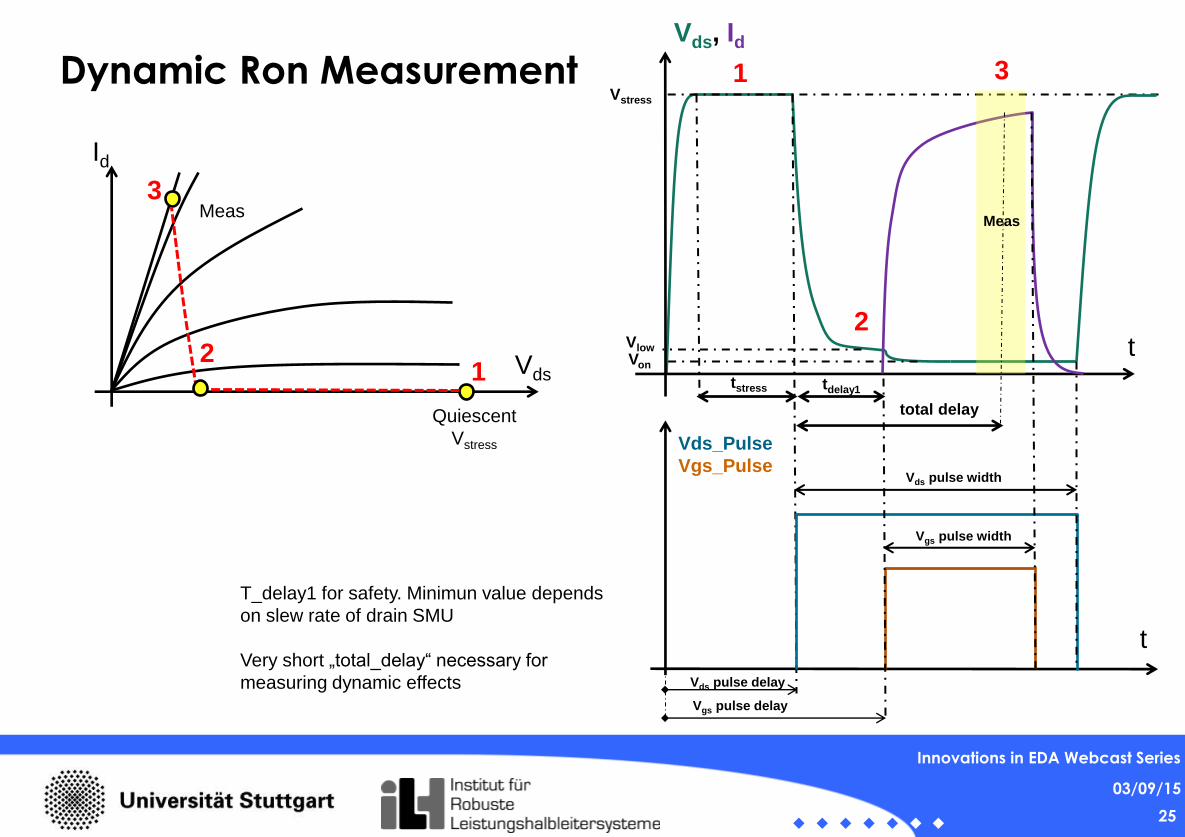
Dynamic Ron Measurement
25
Vstress
Vlow Von
tstress
t
Vds, Id
Quiescent
Vstress
Meas
1 2
3
1
2
3
Meas
Id
Vds tdelay1
Vds pulse delay
Vgs pulse delay
Vds pulse width
Vgs pulse width
T_delay1 for safety. Minimun value depends
on slew rate of drain SMU
Very short „total_delay“ necessary for
measuring dynamic effects
total delay
Vds_Pulse
Vgs_Pulse
t
03/09/15
Innovations in EDA Webcast Series

Trapping Effects in GaN devices
26
03/09/15
Innovations in EDA Webcast Series
0
5
10
15
20
25
0 5 10 15
Id (
A)
Vds (V)
Effect of Vstress in Output Characteristics
V_Stress = 50V
V_Stress = 100V
V_Stress = 150V
V_Stress = 200V
Measurement Setup • VdsPulse_Delay = 1us
• VdsPulse_width = 10us
• VgsPulse_Delay = 1.6us
• VgsPulse_Width = 8us
• Period = 2ms
• NOS = 1
DUT: 600V GaN-on-Si
trapping states in
the off-state affect
Ron in the on-state

Ron vs. Time
27
03/09/15
Innovations in EDA Webcast Series
Measurement Setup • VdsPulse_Delay = 1us
• VdsPulse_Width = 10us
• VgsPulse_Delay = 1.5us
• VgsPulse_Width = 8us
• Period = 2ms
• NOS = 1
• Resolution=200ns
0.2
0.3
0.4
0.5
0.6
0.7
0.8
0.9
0.E+00 1.E-06 2.E-06 3.E-06 4.E-06 5.E-06
Ro
n (Ω
)
Time (seconds)
Vstress = 200V
Vstress = 20V
DUT: 600V GaN-on-Si
SMU slew rate
delay
stable voltages
?

Benchmarking Different GaN Devices
28
03/09/15
Innovations in EDA Webcast Series
0
5
10
15
20
25
30
35
0 2 4 6 8
Id (
A)
Vds (V)
Device A
Device B
Device C
Measurement setup • Same voltage conditions
• VdsPulse_Delay = 1us
• VdsPulse_Width = 10us
• VgsPulse_Delay = 1.5us
• VgsPulse_Width = 8us
• Period = 2ms
• NOS = 1 comparable
devices from
different
manufacturers
Ron Temperature Dependence
29
03/09/15
Innovations in EDA Webcast Series
0
0.05
0.1
0.15
0.2
0.25
0.3
0 20 40 60 80
Ro
n (Ω
)
Ids (A)
Vgs=10V
T=23°C
T=100°C
T=150°C
Measurement Setup • Vgs=10V
• GatePulse_Delay=100us
• GatePulse_Width=100us
• DrainPulse_Delay=0us
• DrainPUlse_Width=200us
• PulsePeriod=50ms
DUT:
SiC MOSFET
600V / 100mΩ / 35A
B1506A w/ heat plate

Model Requirements
• 2D Capacitance Model
• LF Dispersion Model
• Thermal Model
30
03/09/15
Innovations in EDA Webcast Series
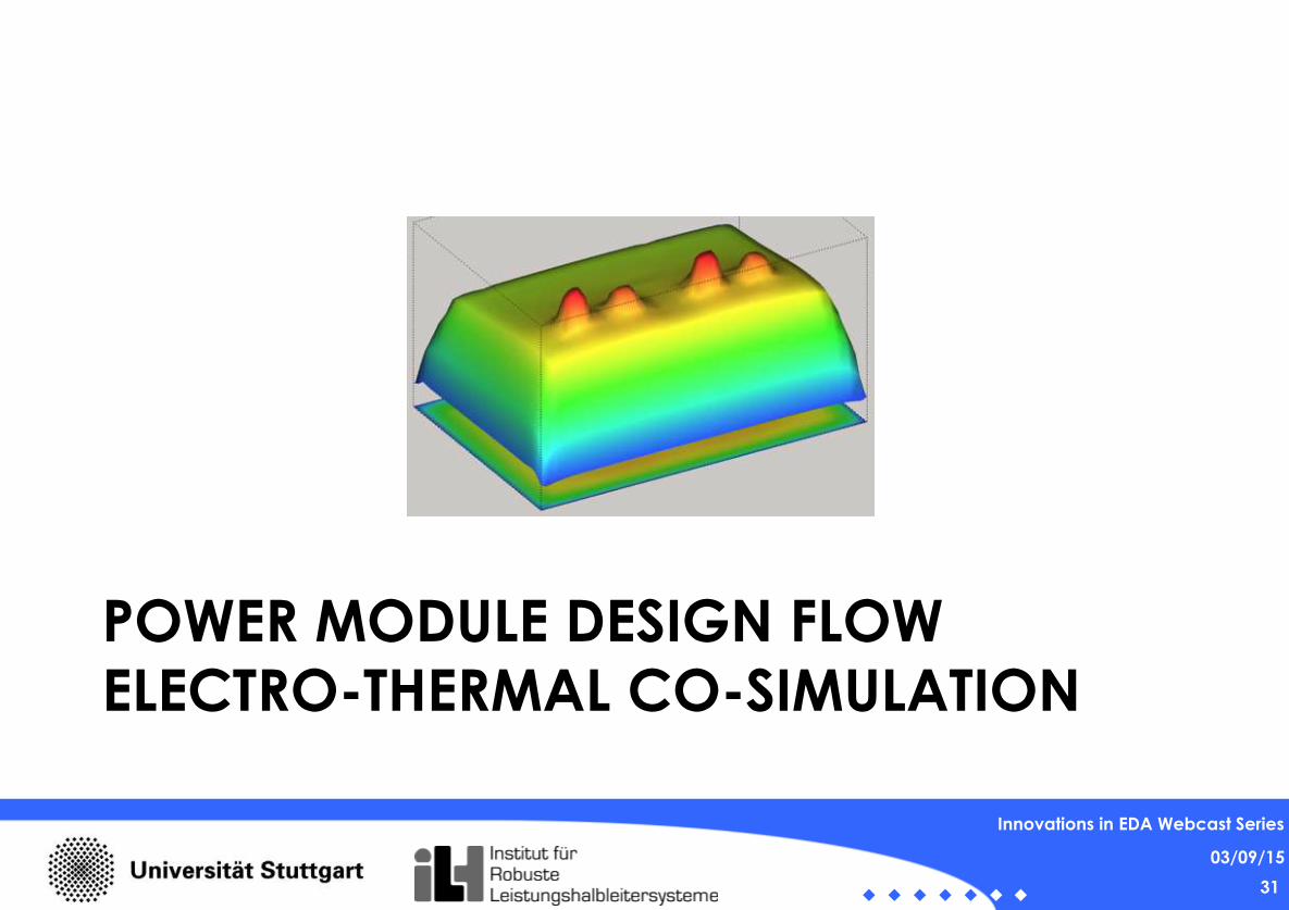
POWER MODULE DESIGN FLOW
ELECTRO-THERMAL CO-SIMULATION
31
03/09/15
Innovations in EDA Webcast Series

SiC MOSFET Multi-Chip
Power Module
32
03/09/15
Innovations in EDA Webcast Series
AlN DBC with half- and full-bridge
• bare-die SiC MOSFETs
• driver ICs
• bootstrap supply
• buffer caps
• fsw > 100 kHz
• power up to 10 kW
• Reliability: 10°C simulated ΔT from Tj to Theatsink
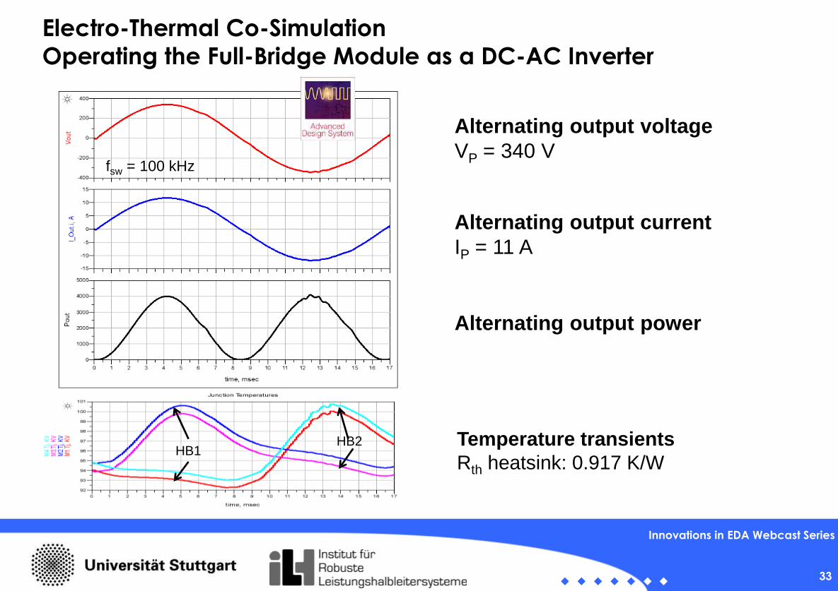
Electro-Thermal Co-Simulation
Operating the Full-Bridge Module as a DC-AC Inverter 03/09/15
Alternating output voltage
VP = 340 V
Alternating output current
IP = 11 A
Alternating output power
Temperature transients
Rth heatsink: 0.917 K/W HB1
HB2
Innovations in EDA Webcast Series
33
fsw = 100 kHz

Fullbridge Module Transient Simulation 03/09/15
Observations
• The temperature in the SiC MOSFETs pulsates with 60 Hz
• Temperature difference about 5 °C
• Temperature peaking is only visible in the junction layer
• Time constants of the materials are high enough
Innovations in EDA Webcast Series
34
Electro-thermal Co-Simulation 03/09/15
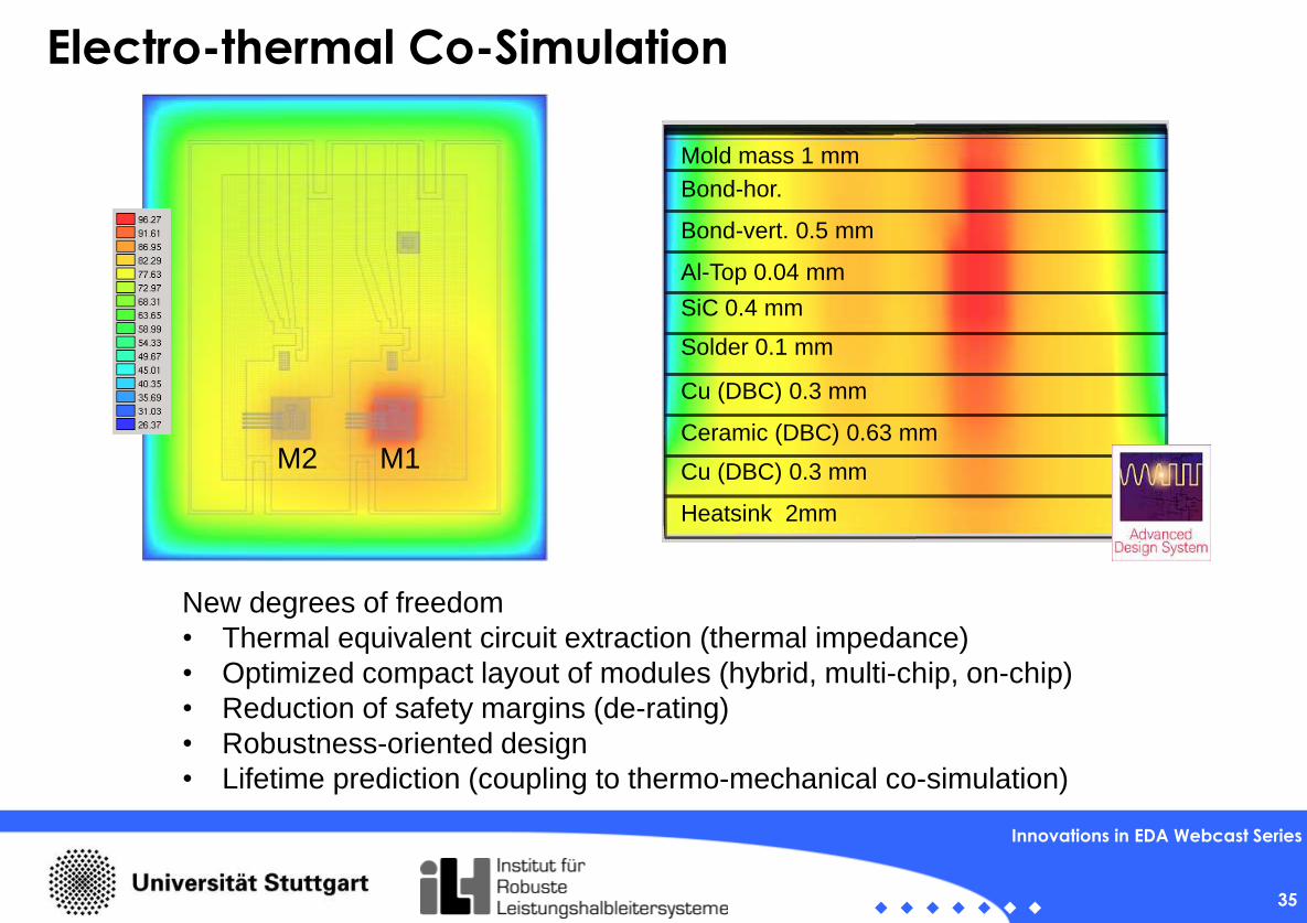
New degrees of freedom
• Thermal equivalent circuit extraction (thermal impedance)
• Optimized compact layout of modules (hybrid, multi-chip, on-chip)
• Reduction of safety margins (de-rating)
• Robustness-oriented design
• Lifetime prediction (coupling to thermo-mechanical co-simulation)
Heatsink 2mm
Cu (DBC) 0.3 mm
Solder 0.1 mm
SiC 0.4 mm
Al-Top 0.04 mm
Bond-vert. 0.5 mm
Ceramic (DBC) 0.63 mm
Cu (DBC) 0.3 mm
Bond-hor.
Mold mass 1 mm
M1 M2
Innovations in EDA Webcast Series
35

POWER MODULE DESIGN FLOW
GAN INTEGRATION
36
03/09/15
Innovations in EDA Webcast Series
AlGaN/GaN HEMTs...
can be tailored for power (Baliga FOM, RonQg,
Vbd) and microwave applications (Johnson FOM,
fmax, Vbd)
show best RonQg compared to Si and SiC
can be cost-efficient when on Si-substrate
as lateral devices are amenable to monolithic
functional integration
are today less mature (traps -> reliability, dynamic
Ron, ...)
are intrinsic depletion-mode / normally-on
devices, normally-off are more complex (p-
doping, Si-GaN cascode, ...)
have limited input dynamic range due to Schottky
gate (except MISFET)
37
03/09/15
Innovations in EDA Webcast Series
600V E-(GI)HEMT
600V D-HEMT
600V E-mode
Si/GaN cascode
650V E-HEMT
600V E-HEMT

GaN Driver Integration: Motivation
38
03/09/15
Innovations in EDA Webcast Series
Quasi normally-off
GaN driver
(Monolithic) Integration of
Gate driver & power transistor
Switching
Speed:
reduction of gate
loop inductance
Robustness:
normally-off
default
behaviour
t
VGS
conventional hybrid assembly
shoot-through
currents
over-shoot
& oscillations
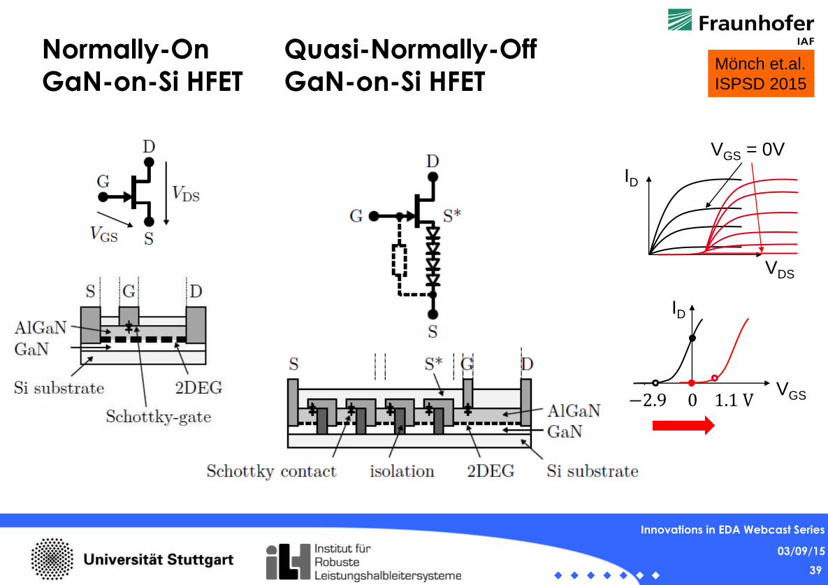
Normally-On Quasi-Normally-Off
GaN-on-Si HFET GaN-on-Si HFET
39
03/09/15
Innovations in EDA Webcast Series
−2.9 0 1.1 V
ID
VGS = 0V
ID
VDS
VGS
Mönch et.al.
ISPSD 2015

Boost Converter
40
03/09/15
Innovations in EDA Webcast Series
GaN 600 V
HFET
GaN gate
driver
VG-
VG++
VOUT VIN
switching
node
Monolithic integration Hybrid integration
Mönch et.al.
ISPSD 2015
• No shoot-through currents
robust
• Default: pull-down
power transistor off
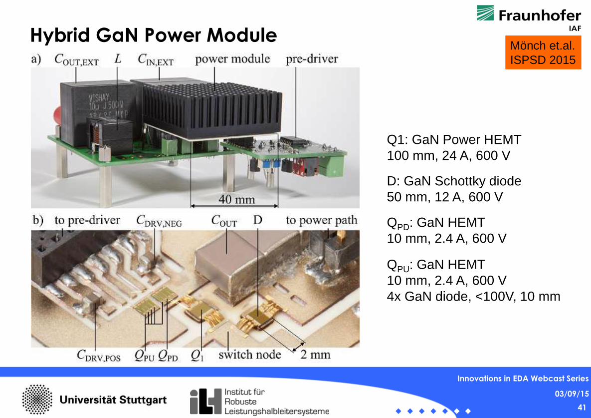
Hybrid GaN Power Module
41
03/09/15
Innovations in EDA Webcast Series
Mönch et.al.
ISPSD 2015
Q1: GaN Power HEMT
100 mm, 24 A, 600 V
D: GaN Schottky diode
50 mm, 12 A, 600 V
QPD: GaN HEMT
10 mm, 2.4 A, 600 V
QPU: GaN HEMT
10 mm, 2.4 A, 600 V
4x GaN diode, <100V, 10 mm

Turn-On and Turn-Off Transitions
Turn-on
tf,DS > 1.6 ns
dV/dtMAX ≈ 91 V /ns
tr,GS ≈ 5.4 ns
no overshoot
no oscillation
fast switching
Turn-off
tr,DS > 1.2 ns
dV/dtMAX ≈ 177 V /ns
tf,GS ≈ 3.8 ns
fast switching
42
03/09/15
Innovations in EDA Webcast Series
Mönch et.al.
ISPSD 2015

Monolithic Integration: Gate Driver & Power
Transistor
Parasitic gate loop
inductance almost eliminated
Monolithic combination of
transistors with different
voltage ratings
Power transistor 600 V / 24 A
Pull-up driver <100 V / 2.4 A
Pull-down driver <100V / -1.2 A
43
03/09/15
Innovations in EDA Webcast Series
3 x
2 m
m2
CONCLUSION
44
03/09/15
Innovations in EDA Webcast Series

45
03/09/15
Innovations in EDA Webcast Series
46
03/09/15
Thank you for your attention
Ingmar Kallfass
University of Stuttgart
Institute of Robust Power Semiconductor Systems
Pfaffenwaldring 47
D – 70569 Stuttgart
Tel.: +49 (0)711-685-68747
Fax: +49 (0)711-685-58747
E-Mail: [email protected]
Innovations in EDA Webcast Series
ILH was founded in the frame of
ILH is a member of
References
[Catrene] Integrated power & energy efficiency, Power device
technologies, simulations, assembly and circuit topographies enabling high
energy efficiency applications, Catrene Scientific Committee Working
Group Integrated power & energy efficiency,
http://www.catrene.org/web/downloads/IPEE_Report_by_Catrene%20Sci._
Comm.pdf
[BIS] UK Department for Business Innovation and Skills, “Power electronics: A
strategy for success,” 2011.
[ECPE] [Online] http://www.ecpe.org/
47
03/09/15
Innovations in EDA Webcast Series
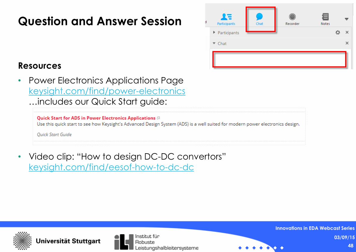
Question and Answer Session
Resources
• Power Electronics Applications Page
keysight.com/find/power-electronics
…includes our Quick Start guide:
• Video clip: “How to design DC-DC convertors”
keysight.com/find/eesof-how-to-dc-dc
48
03/09/15
Innovations in EDA Webcast Series