hotel arasan sapthagiri, madurai january 23, 2011
Post on 22-Dec-2015
220 views
TRANSCRIPT
ICAL ELECTRONICS MEETING
Hotel Arasan Sapthagiri, MaduraiJanuary 23, 2011
B.Satyanarayana, TIFR, Mumbai INO Collaboration Meeting, Madurai January 23-26, 2011
Last ICAL Electronics meeting
Held at IIT Madras, Chennai During August 9-11, 2010 Groups attended: IITM, BARC, SINP and TIFR
B.Satyanarayana, TIFR, Mumbai INO Collaboration Meeting, Madurai January 23-26, 2011
To do list – then! Interconnection between RPC strips and preamp inputs (SINP/TIFR) Problems with FPGA TDC (Hari, Sudeshna) Problem with ASIC TDC (3rd stage interpolation, Pooja) ASIC or FPGA TDC? If FPGA TDC, can we include all other logic (+ data transmitter) into it? Can the 8-in-one FE board have TDC as well?
This automatically means we will have TDC data for all channels. FE output in LVDS? Depends on above Power supplies (LV and HV), distribution and monitoring
Indigenous, commercial, semi-commercial, dc-hvdc (SINP/VECC) Controller (MSP430 TI chip) and data interface from RPC to the backend (IITM)
Data interface: Ethernet, fibre, wire-less Problem regarding FPGA as trigger element (Mandar) Calibration/synchronisation of global signals and data paths Backend standard, alternate to VME, Distributed backend? Trigger system – segmentation (James, Mandar, Sudeshna, Pooja) Trigger-less system: Any takers, on back foot for now? Supernova trigger? Proposed by M.V.N.Murthy Waveform sampler (Nagendra) GPS based RTC

B.Satyanarayana, TIFR, Mumbai INO Collaboration Meeting, Madurai January 23-26, 2011
Agenda for today’s meeting Pickup from where we last left! Try to consolidate at least some areas Agree to responsibilities and timelines Form groups and means of communication Agree on methods and standards Listen to and discuss any new requirements Take more (younger) people on board
B.Satyanarayana, TIFR, Mumbai INO Collaboration Meeting, Madurai January 23-26, 2011
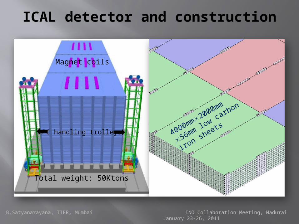
ICAL detector and construction
Magnet coils
RPC handling trolleys
Total weight: 50Ktons
4000mm2000mm
56mm low ca
rbon
iron sh
eets
B.Satyanarayana, TIFR, Mumbai INO Collaboration Meeting, Madurai January 23-26, 2011
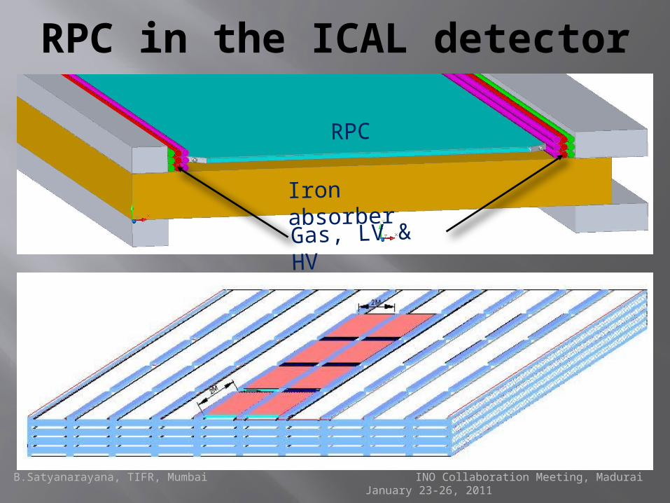
RPC in the ICAL detector
RPC
Iron absorber
Gas, LV & HV
B.Satyanarayana, TIFR, Mumbai INO Collaboration Meeting, Madurai January 23-26, 2011
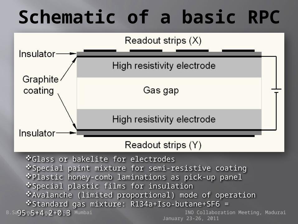
Schematic of a basic RPC
Glass or bakelite for electrodesSpecial paint mixture for semi-resistive coatingPlastic honey-comb laminations as pick-up panelSpecial plastic films for insulationAvalanche (limited proportional) mode of operationStandard gas mixture: R134a+Iso-butane+SF6 = 95.5+4.2+0.3
B.Satyanarayana, TIFR, Mumbai INO Collaboration Meeting, Madurai January 23-26, 2011
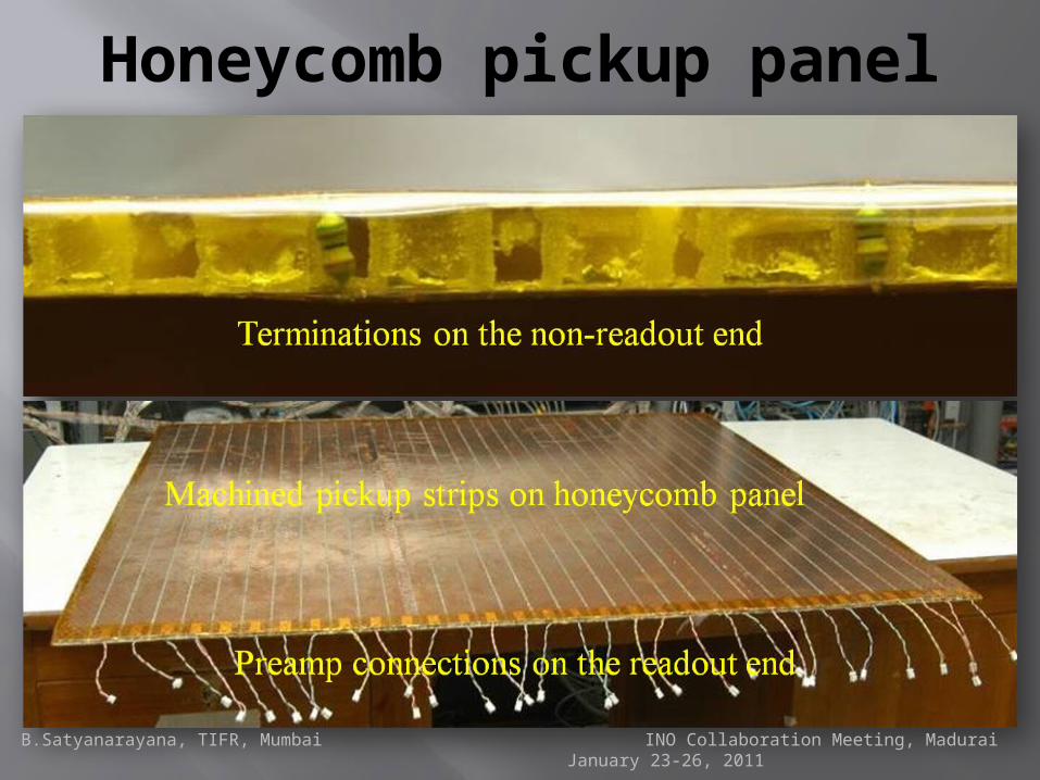
Honeycomb pickup panel
B.Satyanarayana, TIFR, Mumbai INO Collaboration Meeting, Madurai January 23-26, 2011
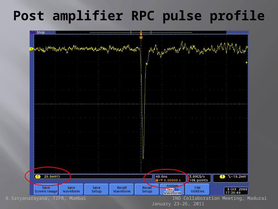
Post amplifier RPC pulse profile
B.Satyanarayana, TIFR, Mumbai INO Collaboration Meeting, Madurai January 23-26, 2011
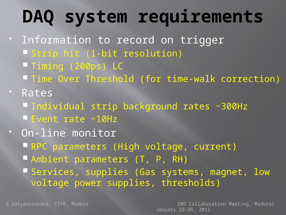
DAQ system requirements Information to record on trigger
Strip hit (1-bit resolution) Timing (200ps) LC Time Over Threshold (for time-walk correction)
Rates Individual strip background rates ~300Hz Event rate ~10Hz
On-line monitor RPC parameters (High voltage, current) Ambient parameters (T, P, RH) Services, supplies (Gas systems, magnet, low
voltage power supplies, thresholds)
B.Satyanarayana, TIFR, Mumbai INO Collaboration Meeting, Madurai January 23-26, 2011
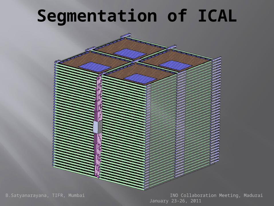
Segmentation of ICAL
B.Satyanarayana, TIFR, Mumbai INO Collaboration Meeting, Madurai January 23-26, 2011
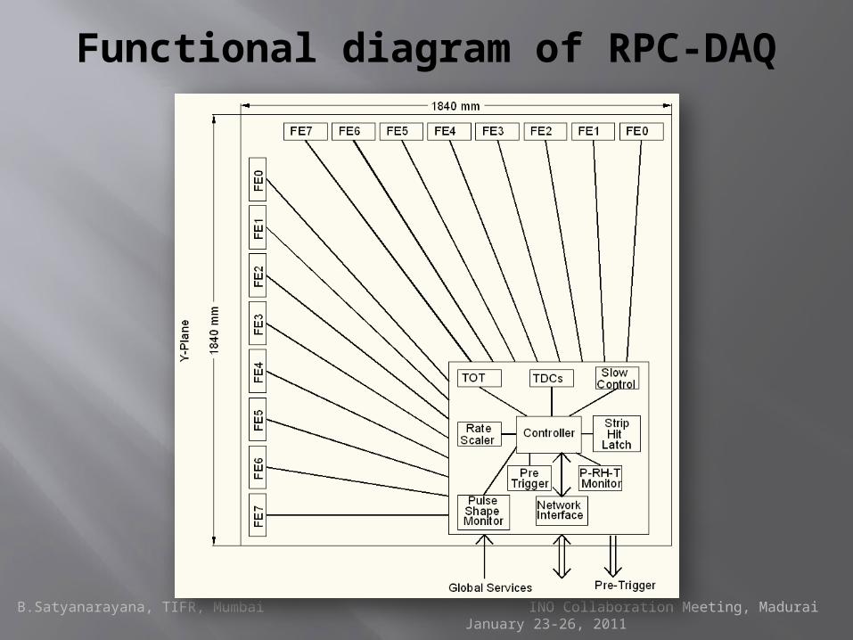
Functional diagram of RPC-DAQ
B.Satyanarayana, TIFR, Mumbai INO Collaboration Meeting, Madurai January 23-26, 2011
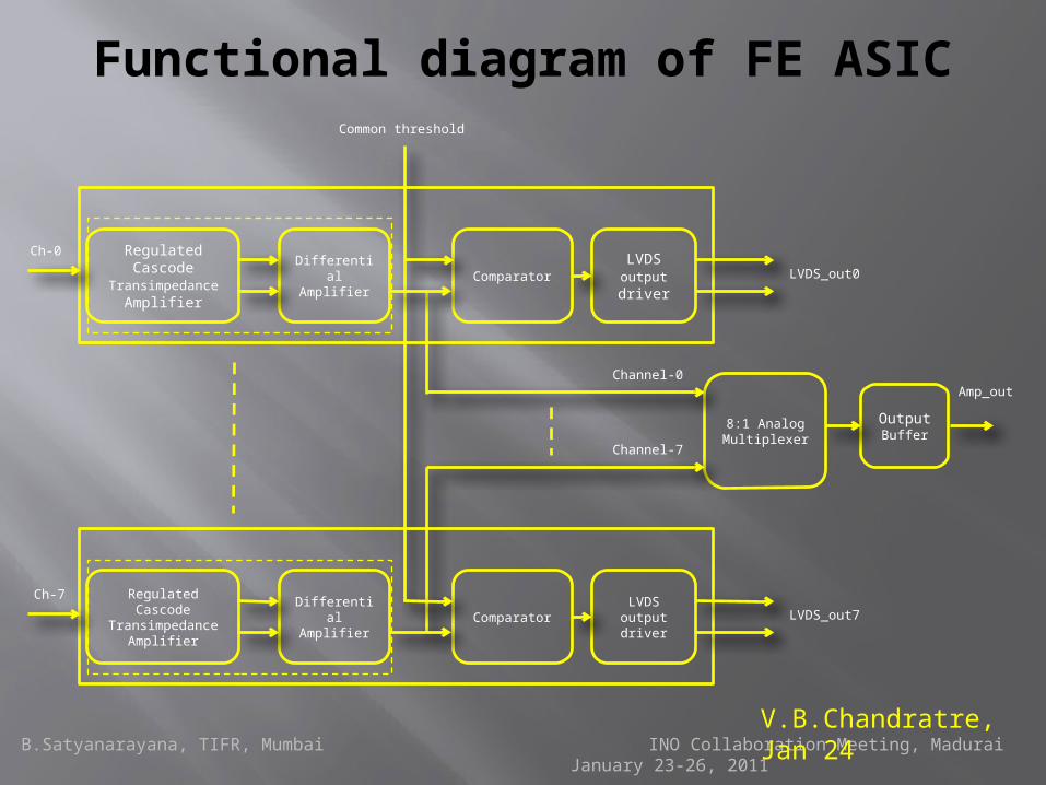
Functional diagram of FE ASIC
Amp_out
8:1 Analog Multiplexer
Channel-0
Channel-7
Output Buffer
Regulated Cascode
Transimpedance Amplifier
Differential Amplifier
ComparatorLVDS output driver
Regulated Cascode
Transimpedance Amplifier
Differential Amplifier
ComparatorLVDS
output driver
Common threshold
LVDS_out0
LVDS_out7
Ch-0
Ch-7
V.B.Chandratre, Jan 24
B.Satyanarayana, TIFR, Mumbai INO Collaboration Meeting, Madurai January 23-26, 2011
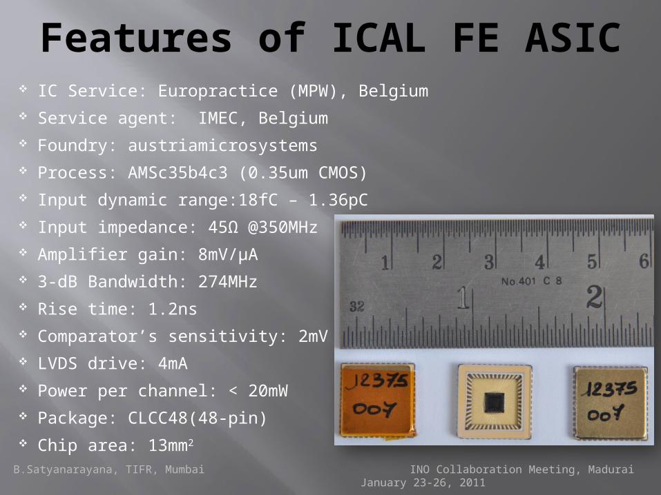
Features of ICAL FE ASIC IC Service: Europractice (MPW), Belgium Service agent: IMEC, Belgium Foundry: austriamicrosystems Process: AMSc35b4c3 (0.35um CMOS) Input dynamic range:18fC – 1.36pC Input impedance: 45Ω @350MHz Amplifier gain: 8mV/μA 3-dB Bandwidth: 274MHz Rise time: 1.2ns Comparator’s sensitivity: 2mV LVDS drive: 4mA Power per channel: < 20mW Package: CLCC48(48-pin) Chip area: 13mm2
B.Satyanarayana, TIFR, Mumbai INO Collaboration Meeting, Madurai January 23-26, 2011
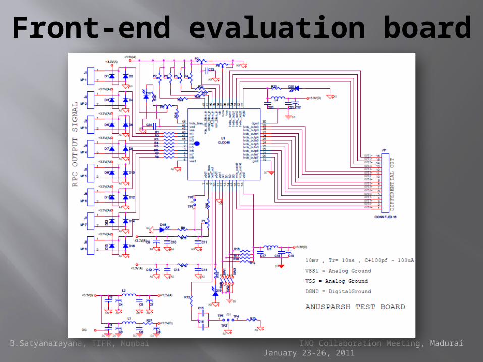
Front-end evaluation board
B.Satyanarayana, TIFR, Mumbai INO Collaboration Meeting, Madurai January 23-26, 2011
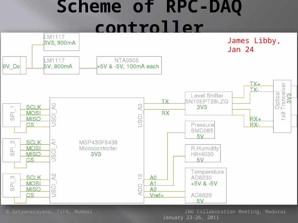
Scheme of RPC-DAQ controller
James Libby, Jan 24
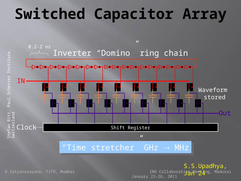
Switched Capacitor Array
B.Satyanarayana, TIFR, Mumbai INO Collaboration Meeting, Madurai January 23-26, 2011
Shift RegisterClock
IN
Out
“Time stretcher” GHz MHz“Time stretcher” GHz MHz
Waveform stored
Inverter “Domino” ring chain0.2-2 ns
Ste
fan R
itt,
Paul Sch
err
er
Inst
itute
, Sw
itze
rland
S.S.Upadhya, Jan 24
B.Satyanarayana, TIFR, Mumbai INO Collaboration Meeting, Madurai January 23-26, 2011
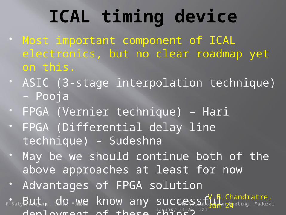
ICAL timing device Most important component of ICAL
electronics, but no clear roadmap yet on this. ASIC (3-stage interpolation technique) – Pooja FPGA (Vernier technique) – Hari FPGA (Differential delay line technique) –
Sudeshna May be we should continue both of the above
approaches at least for now Advantages of FPGA solution But, do we know any successful deployment
of these chips?V.B.Chandratre, Jan 24
B.Satyanarayana, TIFR, Mumbai INO Collaboration Meeting, Madurai January 23-26, 2011
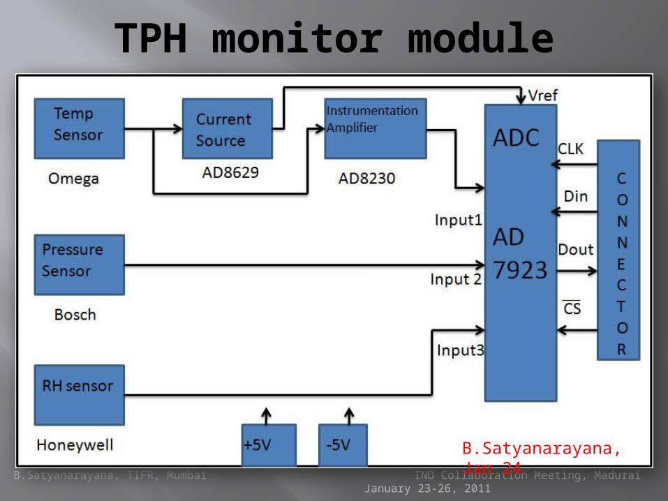
TPH monitor module
B.Satyanarayana, Jan 24
B.Satyanarayana, TIFR, Mumbai INO Collaboration Meeting, Madurai January 23-26, 2011
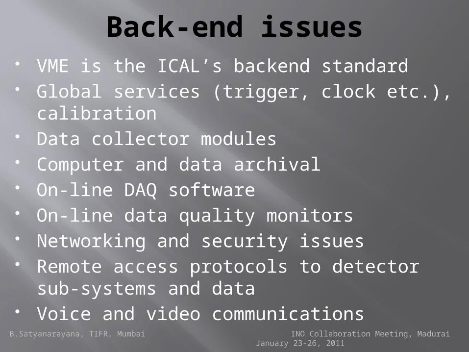
Back-end issues VME is the ICAL’s backend standard Global services (trigger, clock etc.),
calibration Data collector modules Computer and data archival On-line DAQ software On-line data quality monitors Networking and security issues Remote access protocols to detector sub-
systems and data Voice and video communications
B.Satyanarayana, TIFR, Mumbai INO Collaboration Meeting, Madurai January 23-26, 2011
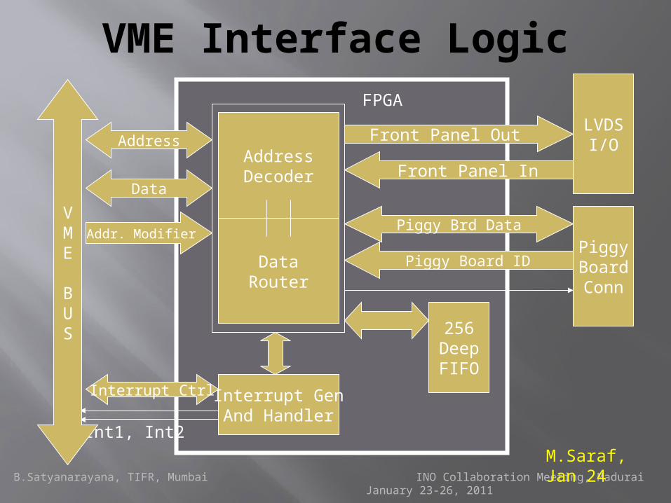
VME Interface Logic
Address
Data
Addr. Modifier
AddressDecoder
DataRouter
FPGA
Front Panel Out
Front Panel In
Piggy Brd Data
Piggy Board ID
LVDSI/O
PiggyBoardConn
Interrupt GenAnd Handler
256DeepFIFO
Int1, Int2
Interrupt Ctrl
VME
BUS
M.Saraf, Jan 24
B.Satyanarayana, TIFR, Mumbai INO Collaboration Meeting, Madurai January 23-26, 2011
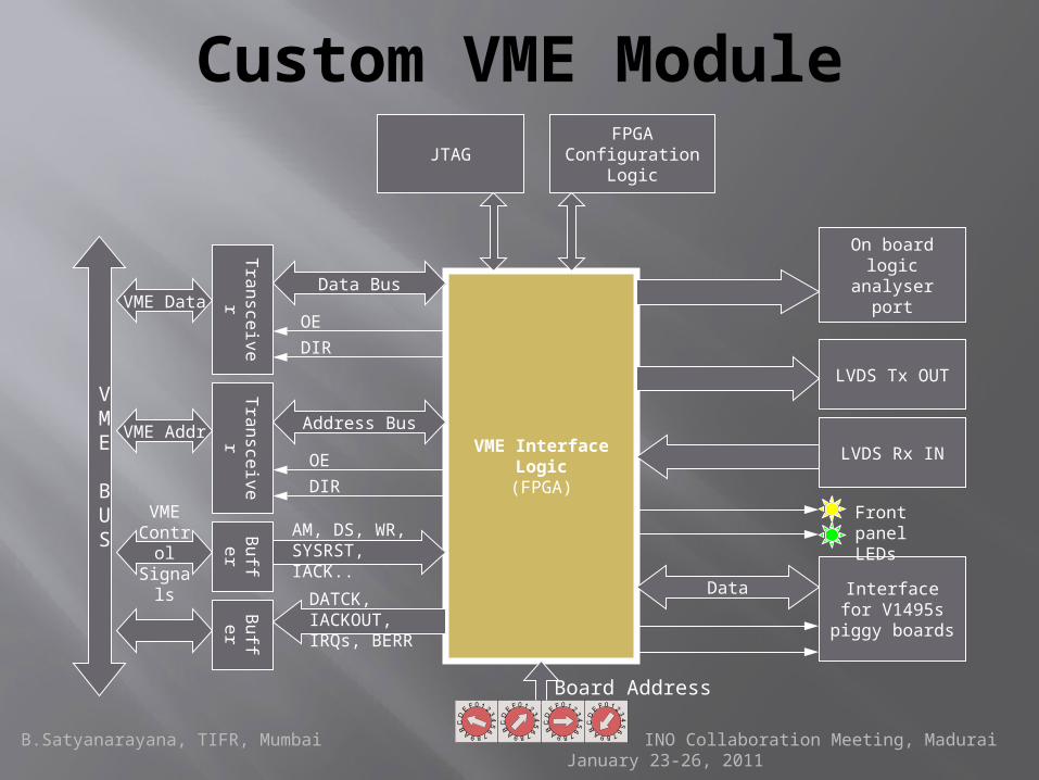
Custom VME Module
VME InterfaceLogic(FPGA)
VME Data
Transce
iver
Data Bus
VME Addr
Transce
iver
Address Bus
JTAGFPGA
Configuration Logic
On board logic analyser port
VME Contr
ol Signal
s
Buff
er
AM, DS, WR, SYSRST, IACK..
Buff
er
VME BUS
LVDS Tx OUT
LVDS Rx IN
Data Interface for V1495s piggy
boards
OE
DIR
OE
DIR
DATCK, IACKOUT, IRQs, BERR
Front panel LEDs
Board Address
B.Satyanarayana, TIFR, Mumbai INO Collaboration Meeting, Madurai January 23-26, 2011
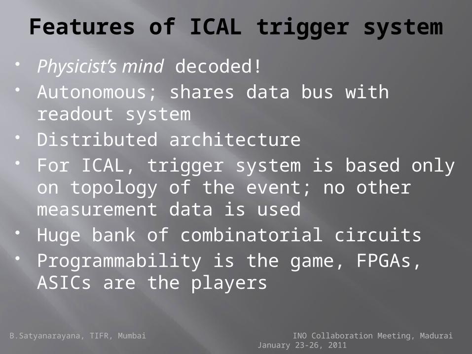
Features of ICAL trigger system
Physicist’s mind decoded! Autonomous; shares data bus with readout
system Distributed architecture For ICAL, trigger system is based only on
topology of the event; no other measurement data is used
Huge bank of combinatorial circuits Programmability is the game, FPGAs, ASICs
are the players
B.Satyanarayana, TIFR, Mumbai INO Collaboration Meeting, Madurai January 23-26, 2011
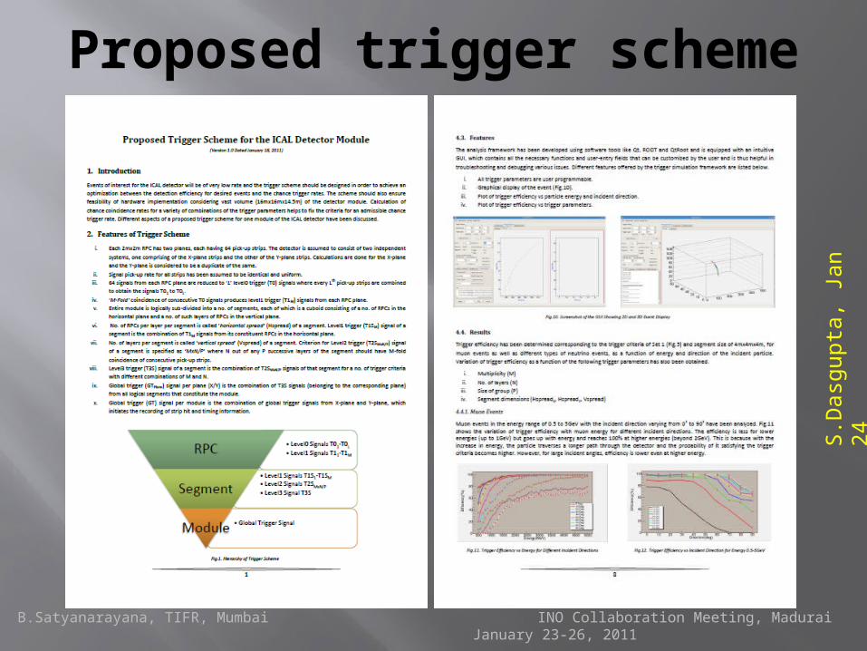
Proposed trigger scheme
S.D
asg
up
ta,
Jan
24
B.Satyanarayana, TIFR, Mumbai INO Collaboration Meeting, Madurai January 23-26, 2011
Power supplies High voltage for RPCs
Voltage: 10kV (nominal) Current: 6mA (approx.) Ramp up/down, on/off, monitoring
Low voltage for electronics Voltages and current budgets still not available at
this time Commercial and/or semi-commercial solutions DC-DC and DC-HVDC converters; cost
considerations
S.Saha, Jan 24
B.Satyanarayana, TIFR, Mumbai INO Collaboration Meeting, Madurai January 23-26, 2011
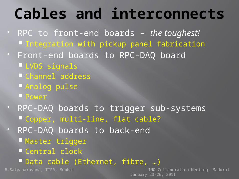
Cables and interconnects RPC to front-end boards – the toughest!
Integration with pickup panel fabrication Front-end boards to RPC-DAQ board
LVDS signals Channel address Analog pulse Power
RPC-DAQ boards to trigger sub-systems Copper, multi-line, flat cable?
RPC-DAQ boards to back-end Master trigger Central clock Data cable (Ethernet, fibre, …)
B.Satyanarayana, TIFR, Mumbai INO Collaboration Meeting, Madurai January 23-26, 2011
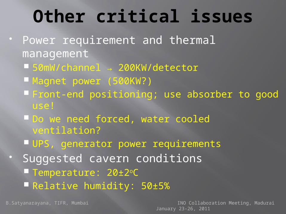
Other critical issues Power requirement and thermal management
50mW/channel → 200KW/detector Magnet power (500KW?) Front-end positioning; use absorber to good use! Do we need forced, water cooled ventilation? UPS, generator power requirements
Suggested cavern conditions Temperature: 20±2oC Relative humidity: 50±5%
B.Satyanarayana, TIFR, Mumbai INO Collaboration Meeting, Madurai January 23-26, 2011
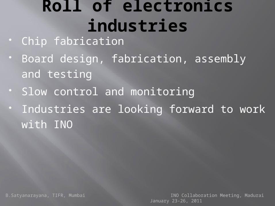
Roll of electronics industries
Chip fabrication Board design, fabrication, assembly and
testing Slow control and monitoring Industries are looking forward to work with
INO
B.Satyanarayana, TIFR, Mumbai INO Collaboration Meeting, Madurai January 23-26, 2011
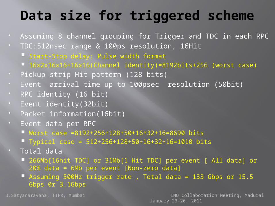
Data size for triggered scheme Assuming 8 channel grouping for Trigger and TDC in each RPC TDC:512nsec range & 100ps resolution, 16Hit
Start-Stop delay: Pulse width format 16x2x16x16+16x16(Channel identity)=8192bits+256 (worst case)
Pickup strip Hit pattern (128 bits) Event arrival time up to 100psec resolution (50bit) RPC identity (16 bit) Event identity(32bit) Packet information(16bit) Event data per RPC
Worst case =8192+256+128+50+16+32+16=8690 bits Typical case = 512+256+128+50+16+32+16=1010 bits
Total data 266Mb[16hit TDC] or 31Mb[1 Hit TDC] per event [ All data] or 20% data
= 6Mb per event [Non-zero data] Assuming 500Hz trigger rate , Total data = 133 Gbps or 15.5 Gbps 0r
3.1Gbps