hongyan liang, hong wei, deng pan and hongxing xu...
TRANSCRIPT

Nanotechnol Rev 2015; 4(3): 289–302
*Corresponding author: Hongxing Xu, Institute of Physics, Chinese Academy of Sciences, and Beijing National Laboratory for Condensed Matter Physics, Beijing 100190, China; and Center for Nanoscience and Nanotechnology, and School of Physics and Technology, Wuhan University, Wuhan 430072, China, e-mail: [email protected] Liang, Hong Wei and Deng Pan: Institute of Physics, Chinese Academy of Sciences, and Beijing National Laboratory for Condensed Matter Physics, Beijing 100190, China
Review
Hongyan Liang, Hong Wei, Deng Pan and Hongxing Xu*
Chemically synthesized noble metal nanostructures for plasmonicsDOI 10.1515/ntrev-2014-0026Received September 6, 2014; accepted April 24, 2015
Abstract: Noble metal nanostructures have drawn atten-tions of researchers in many fields due to their particular optical properties. Controlling the metal nanostructures’ size, shape, material, assembly, and surrounding envi-ronment can tune their unique plasmonic features that are important for practical applications. In this review, we firstly discuss some novel metal nanostructures syn-thesized through wet chemical methods and their funda-mental plasmonic properties. Then, some applications of these chemically synthesized nanostructures in plasmon-ics are highlighted, including surface-enhanced Raman spectroscopy, plasmonic sensing, optical nanoanten-nas, and plasmonic circuitry. Plasmonic nanostructures provide the ways to manipulate light at the nanometer scale and open the prospects of developing nanophotonic devices for sensing and information technologies.
Keywords: nanoantenna; nanowire; plasmonic circuitry; plasmonic sensing; surface-enhanced Raman spectro-scopy; surface plasmons.
1 IntroductionThe surface plasmons (SPs) are the quanta of the plasma oscillations at metal-dielectric interfaces [1]. Under the external time-varying electromagnetic (EM) field, free
electrons in metal will be forced to oscillate collectively against the restoring force of positive nuclei until the energy is lost as a result of resistance or radiation [2, 3]. When an SP combines with a photon, it is called a surface plasmon polariton (SPP). Two types of SPP exist: local-ized surface plasmons (LSPs) and propagating surface plasmons (PSPs) [2, 4]. The LSPs are surface charge oscillations in nanostructures with a size smaller than or comparable with the excitation wavelength in three dimensions. Localized surface plasmon resonance (LSPR) is sensitively dependent on the dielectric environment and the geometry of the nanostructure. When the frequency of the excitation light matches the resonance frequency, the resonance of LSPs occurs, which results in strong light scattering, intense absorption, and giant enhancement of the EM field near the metal nanostructure. The PSPs are surface charge waves propagating in structures with one or two dimensions larger than the wavelength of inci-dent light. They can confine the EM field at the nanom-eter scale and travel along the metal surface up to tens of micrometers [1].
The growing field of researches on maneuvering the SPs in metal nanostructures is known as “plasmonics ” [2, 4]. In this research field, metal nanostructures serve as antennas to convert light into localized electric fields, as sensors to detect the change of the local dielectric environment, and as waveguides to confine and route light beyond the classical diffraction limit. These proper-ties can result in many applications, such as surface-enhanced spectroscopy [5–7], chemical and biochemical sensors [3, 8], nanoantennas [9], nanophotonic circuits [10, 11], optical trapping [12, 13], and super-resolution imaging [14, 15]. With precisely controlled size, shape, and/or spacing of nanostructures, light can be effec-tively manipulated. In the last three decades, a lot of investigations have been focused on the size- and shape-controlled fabrication of nanostructures and the develop-ment of nanofabrication techniques allowing the control of nanostructure geometries and assemblies. A wealth of methods, the bottom-up or the top-down, are available to produce metal nanostructures. Compared with the

290 H. Liang et al.: Chemically synthesized noble metal nanostructures for plasmonics
top-down micro-/nano-fabrication techniques that are usually complicated, costly and time consuming, the wet chemical method is an attractive choice for high-yield, reproducible, and high-throughput syntheses [4].
Noble metal nanostructures have attracted much interest in plasmonic applications because of their good performances. Their ability to support SPs is described by their permittivity. The real part of the permittivity describes the strength of the polarization induced by an external electric field, and this value along with the permittivity of dielectric environment decides the reso-nance frequency. The imaginary part describes the energy losses and damping of the charge oscillations. The noble metals have negative real parts of permittivity, and the resonance frequency of SPs generally falls in the visible spectral range. Moreover, their small imaginary parts of the permittivity make the LSPRs strong with large near-field enhancement, benefiting the corresponding appli-cations. The small imaginary part of the permittivity also leads to low-loss propagating SPs that are important for the applications in nanophotonic circuits. Gold and silver are widely used for plasmonic applications. Gold is often the choice at lower frequencies, having the advantages of being chemically stable in many environments and easy to be fabricated. However, the interband loss of gold in the visible spectral range ( < 500 nm) is high. Among all the noble metal elements, silver has the best performances as silver nanostructures exhibit strong LSPRs tunable over a large wavelength range, wider than that of others. In addi-tion, comparing with gold, silver has a sharper resonance, higher refractive index sensitivity, and is less dissipative. Thus, silver has predominately been the choice for plas-monic applications.
In this review, we mainly focus on silver and gold nanostructures. We will first introduce the nanostruc-tures synthesized by wet chemical methods, including the nanorices, nanocarrots, nanowires (NWs), and so on. In the following, we will discuss some typical investigations about plasmonic applications, which mainly include four aspects: surface-enhanced Raman spectroscopy, plas-monic sensing, optical nanoantennas, and plasmonic circuitry.
2 SPs in chemically synthesized metal nanostructures
Wet chemical procedures that involve the reduction of metal precursors to metal atoms and the controlled aggre-gation of atoms into nanostructures have been proven to
be efficient for reproducible, high-yield, low-cost, and large-scale syntheses to obtain metal nanostructures with excellent plasmonic properties [16]. By this kind of method, many nanostructures can be obtained controlla-bly by tuning the reaction parameters, such as the capping agent, the reaction solution, the reaction time, and the temperature. Scanning electron microscopy (SEM) images of several silver nanostructures produced by wet chemical methods are shown in Figure 1. These nanostructures are spheres [16, 17], cubes [18], bipyramids [19], octahedrons [20], flowers [21], bars [22], rices [22, 23], rods [24], carrots [25], and wires [26]. In the chemical syntheses, the size of the nanostructures is also controllable. For example, the size of silver nanocubes could be tuned from 30 nm to 70 nm by introducing a trace amount of sulfide or hydro-sulfide into reaction solution or by changing silver precur-sors [27]. The length of nanocarrots could be changed from 120 nm to 250 nm by altering the concentration of precur-sors or reaction time [25]. The diameter of NWs could be adjusted from 100 nm to 300 nm by increasing the initial precursor’s concentration [26]. These chemically synthe-sized metal nanostructures can support localized SPs or propagating SPs, and their plasmonic properties are strongly dependent on the geometry and the morphology of the nanostructures. The ability of the chemical synthe-sis methods to control the physical parameters of nano-structures helps to manipulate their plasmonic properties for various applications.
The metal nanostructures of various shapes synthe-sized by chemical methods may support different LSP modes and show abundant plasmonic properties. The simplest spherical nanostructures generally show only one strong LSPR peak that belongs to a family of degen-erate dipole modes. If the symmetry of a nanostructure decreases, the number of LSP modes increases because the structure can support more nondegenerate eigen-res-onances [4, 28]. For example, when the centrosymmetric nanosphere becomes elliptic or forms a quasi-one-dimen-sional (1D) structure, like nanorod [24], nanorice [22, 23], and nanocarrot [25] structures, the decrease in the sym-metry will result in the lifting of mode degeneracy and the growth in the number of LSP modes. The originally degenerate LSP modes in the spherical nanoparticle (NP) now differentiate into transverse and longitudinal modes, as shown in Figure 2. Herein, the plasmon resonances on single NP were excited by the transient field of the elec-trons from a scanning electron probe in the transmis-sion electron microscopy (TEM) system and then imaged by acquiring electron energy loss spectroscopy (EELS) signals. The energy-filtered maps acquired from the rec-tangular region enclosing a nanorice or a nanocarrot are

H. Liang et al.: Chemically synthesized noble metal nanostructures for plasmonics 291
100 nm
A B C D E
F G H I J
100 nm 100 nm 100 nm 500 nm
100 nm 100 nm 100 nm 100 nm 500 nm
Figure 1: Different shapes of silver nanostructures. (A) spheres [17], (B) cubes [18], (C) right bipyramids [19], (D) octahedrons [20], (E) flowers [21], (F) bars [22], (G) rices [23], (H) rods [24], (I) carrots [25], and (J) wires [26]. Reproduced with permission from Refs. [17–26]. Copyright 2010 American Chemical Society (Ref. [17]), Copyright 2002 American Association for the Advancement of Science (Ref. [18]), Copyright 2006 American Chemical Society (Ref. [19]), Copyright 2006 WILEY-VCH Verlag GmbH & Co. KGaA, Weinheim (Ref. [20]), Copyright 2009 WILEY-VCH Verlag GmbH & Co. KGaA, Weinheim (Ref. [21]), Copyright 2007 American Chemical Society (Ref. [22]), Copyright 2009 American Chemical Society (Ref. [23]), Copyright 2011 American Chemical Society (Ref. [24]), Copyright 2013 American Chemical Society (Ref. [25]), and Copyright 2008 American Chemical Society (Ref. [26]).
A B C
D
Figure 2: (A, B) High-order plasmon resonances in nanorice (top, 304 nm long and 64 nm diameter at the center) [29] and nanocarrot (top, 225 nm long and 27 nm diameter at the thicker end) [25] were mapped by selectively filtering the scattering intensity belonging to each peak in the EELS signals. Both scale bars are 100 nm. (C) Nonpolarized dark-field scattering spectra of nanorices of various lengths: 300, 328, 335, 363, 417, 436 nm for curves i–vi, respectively [30]. The width of all these nanorices is about 60 nm at the center. The dash lines are eye guides showing the red shift of the plasmon resonances with the increase in the nanorice length. (D) Depend-ence of LSPR peak positions on nanorice lengths [30]. Black dots: Peak positions of different resonance orders for nanorice particles of different lengths determined from dark-field scattering spectra. Four distinct bands separated by the white dashed lines are apparent, corresponding to four well-defined modes with the order indicated by the value of l. Background: Extinction cross-section of individual nanorice (width of 60 nm) calculated from simulations assuming an effective dielectric surrounding, neff = 1.2585. Incident direction and polarization are both aligned 45° with respect to the symmetry axis of the nanorice. Reproduced with permission from Refs. [25, 29, 30]. Copyright 2012 American Chemical Society (Ref. [29]), Copyright 2013 American Chemical Society (Ref. [25]), and Copyright 2010 American Chemical Society (Ref. [30]).

292 H. Liang et al.: Chemically synthesized noble metal nanostructures for plasmonics
shown in Figure 2A and B. The longitudinal modes of dif-ferent orders are shown clearly [25, 29]. It is interesting that compared to symmetric nanorice structure, the multipolar plasmon resonances over the length of the nanocarrot’s axis is asymmetric, and the resonant plasmonic field shows a compression toward the thinner end [25].
The size of a nanostructure can also influence the plas-monic features, such as the ratio of absorption to scatter-ing, the number of LSP modes, and the peak position of a LSP mode. For small spherical NPs, they generally present one dipole mode when their radius R is much smaller than the wavelength of light as we mentioned before. When R is smaller than ∼50 nm, the LSPR extinction is dominated by absorption [9]. When the size of particles increases, scat-tering becomes more efficient. At the same time, the peak positions of LSPRs are red shifted due to the larger charge separations. Meanwhile, the higher-order LSP modes appear as well. For quasi-1D nanostructures such as silver nanorices [30] and nanocarrots [25], the size dependence is more significant. Their longitudinal LSP modes can be tuned from the visible to near-infrared spectral range by controlling the aspect ratio (length/diameter) [31]. In addition, with increasing aspect ratio, higher-order LSP modes can be excited [29, 30, 32–34]. In Figure 2A and B, higher-order LSPRs in a single nanorice and nanocarrot were mapped by selectively filtering the scattering inten-sity belonging to each peak in the EELS signal. From the energy-filtered maps, the standing wave patterns of dif-ferent orders were observed across the long axis of the nanorice and nanocarrot, resulting from the interference of counter-propagating longitudinal plasmon waves. By changing the length of the quasi-1D nanostructure, the resonance peaks can be tuned [29, 30]. Experimentally measured nonpolarized dark-field scattering spectra of individual nanorice particles of various dimensions are shown in Figure 2C. Increasing the length of the parti-cle, the second- and third-order resonance peaks become red shifted. From the simulated results in Figure 2D, we can clearly see that apart from the red shift of the reso-nances, the amplitudes of the LSPRs are increased with the increase in the nanorice length [30]. The nanocarrot structures show a behavior qualitatively similar to that of the nanorice structures [25].
The chemically synthesized NWs have good perfor-mances in supporting PSPs and are widely used for sub-wavelength waveguiding. Compared with NWs fabricated by the complicated and costly top-down methods, the chemically synthesized NWs have high crystallinity and smooth surface, so that they can support PSPs with lower scattering loss and longer propagation distance [10, 11, 35, 36]. The PSPs in chemically synthesized Ag NWs have
been intensively investigated. Owing to the momentum mismatch, the excitation laser from the air side must be focused on the end or other discontinuities of the NW to excite the PSPs [37, 38]. The excited SPs in Ag NW propa-gate forth and back between two ends, making the NW behave like a Fabry-Pérot resonator [39, 40]. The PSPs in Ag NWs are dependent on the NW end shape [41], the cross-section shape [42, 43], the diameter [44, 45], the dielectric environment [44–46], the substrate [43, 47], and the NW bending [48].
3 Plasmonic applicationsNumerous applications based on plasmonics have emerged, which can be assigned to four main catego-ries: (i) concentrating light into localized electric fields to enhance or modify the optical processes of nearby report-ers, such as surface-enhanced spectroscopy [6, 7, 49]; (ii) exploiting the sensitivity of nanostructures’ PSPs or LSPRs to their local dielectric environments for chemi-cal and biochemical sensing and detection [3, 50–52]; (iii) acting as optical nanoantennas to control light at nanoscale [9, 53]; (iv) using PSPs to confine and guide light for plasmonic circuitry [10, 54]. Herein, some typical applications are discussed as follows.
3.1 Surface-enhanced Raman spectroscopy
The metal nanostructures supporting SPs have the ability to focus and manipulate light at the nanometer scale. In general, the excitation of SPs in metal nanostructures can concentrate light into very small volumes, which can alter the excitation and emission of nearby emitters. A typical example is surface-enhanced Raman scattering (SERS). Raman scattering is inelastic scattering of light as a result of its interaction with matter. Raman spectroscopy is used as a powerful tool for chemical analysis, which gives spec-tral fingerprints characteristic of Raman active substances and is sensitive to composition, bond strength, environ-ment, and structure of the analytes. For molecules, the spontaneous Raman scattering is extremely weak due to the small Raman scattering cross section. As a result, it requires a large number of molecules to be involved for detection. In the 1970s, the SERS effect was observed on rough metal surfaces [55]. The main mechanism of SERS is the EM field enhancement in metal nanostructures, which results from the excitation of SPs. As the Raman enhance-ment is roughly proportional to (E/E0)4, where E and E0 are

H. Liang et al.: Chemically synthesized noble metal nanostructures for plasmonics 293
the amplitudes of the local electric field and the original excitation field, respectively, the Raman intensity can be enhanced by billions of times. Therefore, SERS can have the sensitivity of single-molecule detection [6, 7]. The dominating contribution of the EM field enhancement to SERS has made it the main factor to be considered for designing SERS substrates.
Metal nanostructures and rough metal surfaces are widely used as substrates for SERS applications. For nano-structures, the formation of nanogaps between two NPs can dramatically enhance the local EM field through the near-field coupling effect. These nanogaps are also called “hot spots”. To achieve the largest enhancement, the dis-tance between the two particles is required to be below several nanometers. In addition, the incident electric field
should be polarized parallel to the axis of the dimers or multiple particle chains [56]. It should be noted that when the nanogap becomes narrower than half a nanometer, the field enhancement is dramatically reduced due to quantum tunneling effect [57]. SERS substrates involving nanogaps have been fabricated by either bottom-up or top-down processes. For example, dimers and trimers con-sisting of gold NPs synthesized by a wet chemical method are shown in Figure 3A [58]. The simulated distributions of the local electric field enhancement of single particle, dimer, and trimer are shown in Figure 3B–D, respec-tively. Compared with single NP, a dramatic electric field enhancement is observed in the dimer and trimer under the excitation with parallel polarization, which will result in a higher SERS intensity. In fact, dimers have been used
A B
C
D
E F
180
250 nm
0
632.8 nm
kE
Log (E2)
10
8
6
4
2
0
Figure 3: (A) SEM image of gold NPs [58]. Dimers and trimers are highlighted by yellow and green circles, respectively. Inset: TEM image of the nanogap between two NPs. (B–D) Images of the simulated distributions of |E|2 in logarithmic scale with 632.8 nm excitation for single gold NP, dimer, and trimer [58]. (E) SEM image of a dimer consisting of two flower-like silver particles [59]. The dimer axis is rotated about 120° with respect to a horizontal line. (F) Polar plot of the Raman intensity as a function of incident polarization [59]. Reproduced with permission from Refs. [58] and [59]. Copyright 2013 AIP Publishing LLC (Ref. [58]), and Copyright 2012 WILEY-VCH Verlag GmbH & Co. KGaA, Weinheim (Ref. [59]).

294 H. Liang et al.: Chemically synthesized noble metal nanostructures for plasmonics
widely for SERS because by reducing the gap distance, they can generate “hot spots” with very high electric field enhancement, enabling even single-molecule detection by SERS [6, 7]. Not only dimers composed of spherical NPs but also composite systems consisting of nonspheri-cal nanostructures can produce high EM enhancement in the formed nanogaps. For example, the dimers composed of a NP and a nanohole, a NP and a NW, or a NP and a film were demonstrated to be excellent SERS substrates [60–63].
The rough surface topography is another favorable feature for SERS. In these rough structures, the coupling between adjacent protrusions or grooves can generate a large “hot spot” area that facilitates SERS dramatically. Most of the SERS investigations in the early years were based on flat metal surface with roughness. However, the enhancement based on the low-quality rough surface is small, which limits its further application in SERS. With the recent advances in nanofabrication, several kinds of highly rough plasmonic structures were produced control-lably, such as silver flower-like particles and rough silver NWs [60]. Individual flower-like silver microparticles with rough surface can provide vast “hot spots” over the whole particle surface, which makes them have excellent perfor-mance in SERS [21]. The EM enhancement is less depend-ent on the incident polarization because it originates from the nanoscale protrusions and crevices on the randomly textured surface. When two flower-like silver particles formed a dimer as shown in Figure 3E, the SERS inten-sity was further increased by 10∼100 times. The depend-ence of the SERS intensity in this dimer on the incident polarization is shown in Figure 3F, which reveals that the significant additional SERS enhancement is caused by the plasmon coupling effect in the dimer [59]. Owing to the micron-scale size, the flower-like silver particles could be manipulated using a tip under optical microscope [59]. The use of the micro-manipulation allows assembling such kind of large-size particles for larger Raman enhancement factor, which can benefit SERS applications.
The direct contact of metal surface and molecules may cause interaction between them, which may disturb the original Raman signals of the molecules. To avoid direct contact between metal and molecules, some novel SERS substrates have been developed. Li et al. prepared gold NPs with an ultrathin silica or alumina shell for SERS [64]. Spreading such NPs over the probed surface, the Raman signal of analytes could be enhanced and detected. This scheme expands the flexibility of SERS for practical appli-cations. It should be noted that the coupling between two nanoshell-coated Au or Ag NPs can generate hugely enhanced electric field to enable single-molecule SERS
detection, which has been theoretically investigated [65]. Xu et al. reported graphene-mediated SERS substrate, in which the metal nanostructures with hot spots were covered by a monolayer graphene [66]. These shell- or gra-phene-isolated SERS substrates can exclude the Raman signals arising from the interaction between metal surface and molecules, so that clear SERS spectra of the mol-ecules can be obtained. In order to avoid the direct laser illumination, Fang et al. reported remote-excitation SERS [67]. By exciting the propagating SPs in Ag NW, the Raman signal at the locations microns away from the laser spot was remotely excited. By this way, the destruction of the analytes caused by the high-power laser can be reduced, and the signal-to-noise ratio can be improved. Recently, this technique was used for remote excitation and remote detection of single quantum dot (QD) fluorescence [68].
3.2 Plasmonic sensing
Plasmonic sensing enabled by the sensitive response of SPs to local environments has seen prosperous growth in recent years, which has been largely exploited for bio-logical and diagnostic applications [3]. This technique has been commercialized on metal film that can support PSPs. The surface of the metal film is usually functional-ized by a monolayer of special molecules, and then, the film is immersed into the solution of analytes. If the mol-ecules in the solution bind with those on the film, the refractive index of the film surface is altered. By monitor-ing the change of SP resonances, the change of the refrac-tive index is detected. The PSPs in metal NWs can also be used for sensing [44, 51]. The near-field distribution and the output spectra of Ag NW are sensitive to the refractive index of the surrounding medium, which can be used to realize NW-based sensor. Plasmonic sensing using LSPRs in metal NPs has been intensively studied in recent years. In general, NPs are first dispersed in solution or immobi-lized on substrates and inserted into solution later, and then, the extinction or scattering spectra of the solution with plasmonic NPs are measured. By monitoring the LSPR peak shifts, the variation of the refractive index of the solution can be measured.
Compared with spherical NPs, quasi-1D NPs, such as nanorods, nanorices, and nanocarrots, can have higher sensitivity to the local environment change [25, 29, 30, 50, 69]. Sekhon et al. calculated the sensitivity for quasi-1D NPs of Au, Ag, and Cu with different aspect ratios [70]. With the increase in the aspect ratio, the sensitivity is increased, in general. For a monolayer Ag nanorice film on the glass slide, the absorption peak of the longitudinal

H. Liang et al.: Chemically synthesized noble metal nanostructures for plasmonics 295
mode (the peak at long wavelength) is dramatically red shifted when the surrounding medium is changed from air to n-hexane, as shown in Figure 4 [29]. By replacing the medium with ones of higher refractive index, like toluene and carbon disulfide, the longitudinal peak is red shifted further. Figure 4 also shows that the shift of the transverse peak (the peak at about 400 nm wavelength) is much smaller when the dielectric medium is changed. It is noted that the sensitivity of the nanostructures’ LSPRs toward the environmental refractive index change is determined by how easily the mobile free electrons are displaced relative to the fixed positive ion cores under the excitation of light. When the dielectric constant of the medium increases, the Coulombic restoring force on the free electrons in the plasmonic nanostructures is screened more. The LSPR energy reduces as a result of the reduced restoring force, which results in a red shift of the LSPR peak. Both the net polarizability and the specific shape can affect the displacement pattern of the free electron cloud in the metal nanostructures and, thus, influence the sensitivity of LSPRs to the dielectric environment [50].
Usually, the amount of LSPR peak shift per refractive index unit (RIU) change is defined to quantify the detec-tion sensitivity, which is a key factor in determining the performance of the sensor in practical applications. In addition, by taking the peak width into account, the sen-sitivity can be described by a figure of merit (FOM) that is defined as the ratio of the LSPR peak shift per RIU to the full width at half maximum of the LSPR peak [3]. Hence, a narrower peak width can mean a better sensing per-formance. In order to improve the FOM, plasmon modes
0.12
600
400
Transverse resonancesLongitudinal resonances
Airn-hexaneTolueneCarbon disulfide
200Pea
k sh
ifts
(nm
)
Abs
orba
nce
(a.u
.)
0
0.08
0.04
0400 1.0 1.2 1.4
Refractive index (n)1.6800 1200
Wavelength (nm)1600 2000
Figure 4: LSPR sensing using silver nanorice particles with the average aspect ratio ≈5 [29]. Left: absorption spectra of a mon-olayer nanorice film on glass slide immersed in different dielectric media. Right: peak shift of transverse and longitudinal LSPRs as a function of the medium refractive index. The LSPR sensitivities for the longitudinal and transverse modes are 820.6 and 47.3 nm/RIU, respectively. Reproduced with permission from Ref. [29]. Copyright 2012 American Chemical Society.
with a narrow linewidth are exploited, such as multipo-lar LSPRs and Fano resonances [30, 34, 69, 71]. Fano reso-nance resulting from the coherent interference between a dark and a bright plasmon mode is ultrasensitive to the change in local medium, due to a sharp drop in one side of the resonance peak. Theoretical investigations showed that Fano resonances in a nanorod and a nanocube could be employed for refractive index sensing with high FOM [69, 71].
3.3 Optical nanoantennas
Plasmonic nanostructures can work as optical antennas to collect and transmit EM waves at optical frequencies. When a molecule is located in the nanogap between two NPs, the emission direction of its SERS signal will be per-pendicular to the dimer axis, corresponding to a dipole polarized along the dimer axis [72]. Apart from emission direction, the polarization of the emitted light can also be manipulated by the NP antenna [53]. Figure 5A–C shows the results of SERS measurements for a single molecule located in the nanogap of a Ag NP dimer. The maximum Raman intensity is obtained when the inci-dent laser is polarized along the dimer axis as shown in Figure 5B. The emission polarization of the SERS signal is analyzed using the depolarization ratio that is defined as the ratio of the intensity difference of two orthogonally polarized Raman signal to their intensity sum. Figure 5C shows that the maximum depolarization ratio is achieved for incident polarization parallel to the dimer axis. The maximum value ±1 of the depolarization ratio means that the Raman signal is linearly polarized in this case. The polarization behavior of the SERS signal from a dimer is independent of wavelength. For the single-molecule SERS in a trimer structure (Figure 5D), the results become dif-ferent. The strongest intensity of Raman scattering does not correspond to laser polarization along the axis of any two particles as shown in Figure 5E. Based on calcula-tion, the molecule was determined to be located in the junction between particles 2 and 3. Although the depend-ence of Raman intensity on incident polarization is wave-length independent, the depolarization ratio shows a clear dependence on wavelength. As shown in Figure 5F, the depolarization ratio plots for 555 nm and 583 nm Raman signals are shifted from each other. In addition, the maximum of depolarization ratio cannot reach ±1, which indicates that the Raman scattering light is ellipti-cally polarized. Theoretical studies show that the size and location of the third particle can strongly affect the fea-tures of emission polarization in the trimer system. The

296 H. Liang et al.: Chemically synthesized noble metal nanostructures for plasmonics
1.0A
D
B
E
C
F
1.0
1.0
0.5
0.5
-0.5
-0.5
150
12090
60
30
0
330
300270
240
210
180-1.0
0
0
0.8
0.6
Rel
ativ
e in
tens
ity
ρ(θ)
1.0
1.0
0.5
0.5
-0.5
-0.5
150
12090
60
30
0
330
300270
240
210
180-1.0
0
0
ρ(θ)
0.4
0.2
0
1.0
0.8
0.6
Rel
ativ
e in
tens
ity
0.4
0.2
0
0 60 120 180 240 300 360
θ (°)
0 60 120 180 240 300 360
θ (°)
Figure 5: Polarization responses of NP dimer and trimer [53]. (A) A SEM image shows a dimer of Ag NPs, which is tilted about 40° from the vertical direction. (B) Normalized Raman scattering intensity at 555 nm (black squares) and 583 nm (red circles) as a function of the rotation angle of the incident polarization. The green line is the result of generalized Mie theory calculation of the normalized local field enhance-ment factor at 532 nm excitation. (C) Depolarization ratio measured at 555 nm (black squares) and 583 nm (red circles). Black and red lines show the results of Mie theory calculations performed at 555 and 583 nm, respectively. (D–F) Corresponding data for a NP trimer. The red arrow in (D) indicates the position of the molecule that leads to the best agreement between experiment and calculation. Reproduced with permission from Ref. [53]. Copyright 2008 National Academy of Sciences, USA.
polarization manipulation can also be realized in more complex aggregated NP antennas [73]. To realize the polar-ization rotation, the nanoantenna is required to break the dipolar symmetry of the dimer structure. In addition to the geometrical parameters, the refractive index of the surrounding medium can also influence the polarization rotation property of asymmetric nanoantennas [73].
3.4 Plasmonic circuitry
Traditional electronic integrated circuits will soon reach the physical limit in speed. Compared with electrons, taking photons as information carriers has advantages in speed, capacity, and bandwidth. Integrating optical and electronic circuits could provide a possible choice for future information processing [10]. However, the integra-tion of photonic devices is restricted by their large foot-prints, and the further miniaturization is not feasible due to the diffraction limit of light in the dielectric optical devices. Fortunately, plasmonic nanostructures that can carry both optical signals and electric currents could over-come this problem. With the ability to support PSPs and concentrate EM energy into nanoscale volume, plasmonic nanostructures enable the manipulation of light beyond
the diffraction limit. The plasmonic circuitry with a size comparable to the optical wavelength is possible to be used for tomorrow’s information technology.
As the cornerstone of plasmonic circuitry, plasmonic waveguides have been studied intensively. The flexible modulation of the PSP field distribution on Ag NW is shown in Figure 6A [74]. The Ag NW was coated by a layer of QDs with Al2O3 as spacer between them [Figure 6A (ii)]. When one end of the NW was illuminated by the focused laser, the light would couple to the SP modes and propa-gate along the NW [Figure 6A (iii)]. As the intensity of plasmon-induced QD fluorescence is proportional to the local field intensity, the QD fluorescence can be used to image the near-field distributions, as shown in Figure 6A (iv–vii). For a NW on substrate, usually only the three lowest-order modes H0, H1, and H2 should be considered for the realistic NW, with higher-order modes cut-off [35, 44]. The components of the generated plasmon modes in the NW are determined by the polarization of the laser. When the laser is polarized parallel to the NW, only H0 and H2 modes can be excited. The superposition of these two modes results in the periodic symmetric field distri-bution in Figure 6A (iv). When the laser is polarized per-pendicular to the NW, only H1 mode can be excited with symmetric field distributed mainly on the two sides of the
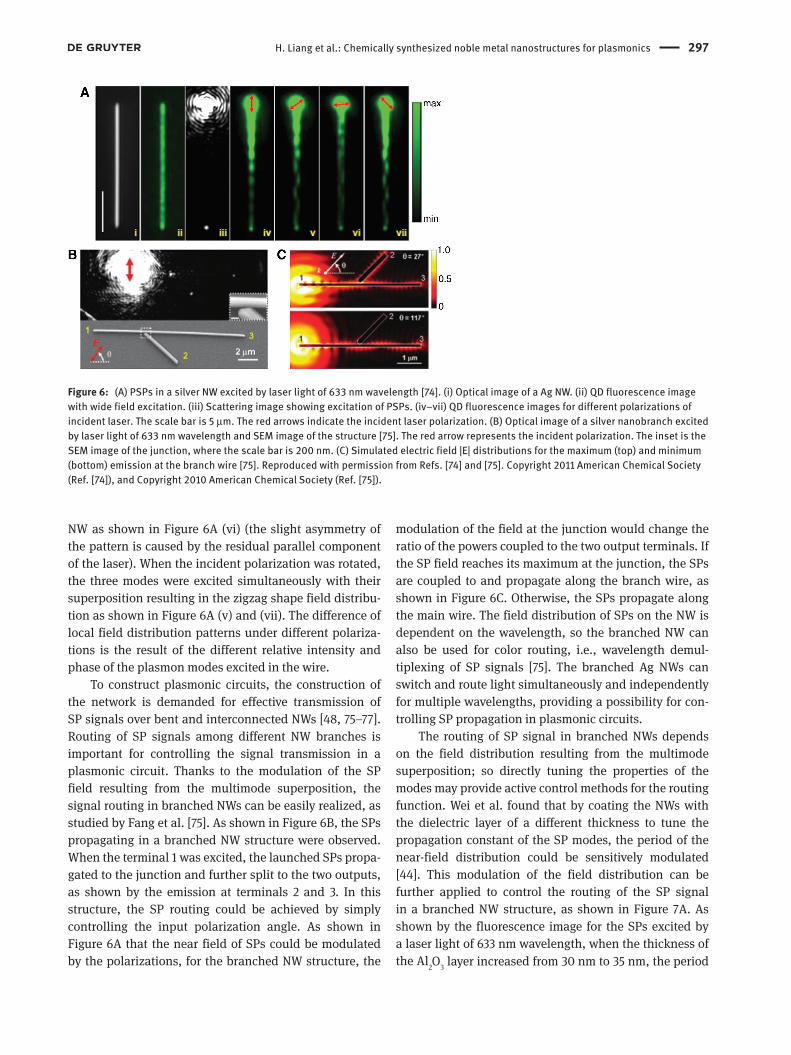
H. Liang et al.: Chemically synthesized noble metal nanostructures for plasmonics 297
NW as shown in Figure 6A (vi) (the slight asymmetry of the pattern is caused by the residual parallel component of the laser). When the incident polarization was rotated, the three modes were excited simultaneously with their superposition resulting in the zigzag shape field distribu-tion as shown in Figure 6A (v) and (vii). The difference of local field distribution patterns under different polariza-tions is the result of the different relative intensity and phase of the plasmon modes excited in the wire.
To construct plasmonic circuits, the construction of the network is demanded for effective transmission of SP signals over bent and interconnected NWs [48, 75–77]. Routing of SP signals among different NW branches is important for controlling the signal transmission in a plasmonic circuit. Thanks to the modulation of the SP field resulting from the multimode superposition, the signal routing in branched NWs can be easily realized, as studied by Fang et al. [75]. As shown in Figure 6B, the SPs propagating in a branched NW structure were observed. When the terminal 1 was excited, the launched SPs propa-gated to the junction and further split to the two outputs, as shown by the emission at terminals 2 and 3. In this structure, the SP routing could be achieved by simply controlling the input polarization angle. As shown in Figure 6A that the near field of SPs could be modulated by the polarizations, for the branched NW structure, the
modulation of the field at the junction would change the ratio of the powers coupled to the two output terminals. If the SP field reaches its maximum at the junction, the SPs are coupled to and propagate along the branch wire, as shown in Figure 6C. Otherwise, the SPs propagate along the main wire. The field distribution of SPs on the NW is dependent on the wavelength, so the branched NW can also be used for color routing, i.e., wavelength demul-tiplexing of SP signals [75]. The branched Ag NWs can switch and route light simultaneously and independently for multiple wavelengths, providing a possibility for con-trolling SP propagation in plasmonic circuits.
The routing of SP signal in branched NWs depends on the field distribution resulting from the multimode superposition; so directly tuning the properties of the modes may provide active control methods for the routing function. Wei et al. found that by coating the NWs with the dielectric layer of a different thickness to tune the propagation constant of the SP modes, the period of the near-field distribution could be sensitively modulated [44]. This modulation of the field distribution can be further applied to control the routing of the SP signal in a branched NW structure, as shown in Figure 7A. As shown by the fluorescence image for the SPs excited by a laser light of 633 nm wavelength, when the thickness of the Al2O3 layer increased from 30 nm to 35 nm, the period
Figure 6: (A) PSPs in a silver NW excited by laser light of 633 nm wavelength [74]. (i) Optical image of a Ag NW. (ii) QD fluorescence image with wide field excitation. (iii) Scattering image showing excitation of PSPs. (iv–vii) QD fluorescence images for different polarizations of incident laser. The scale bar is 5 μm. The red arrows indicate the incident laser polarization. (B) Optical image of a silver nanobranch excited by laser light of 633 nm wavelength and SEM image of the structure [75]. The red arrow represents the incident polarization. The inset is the SEM image of the junction, where the scale bar is 200 nm. (C) Simulated electric field |E| distributions for the maximum (top) and minimum (bottom) emission at the branch wire [75]. Reproduced with permission from Refs. [74] and [75]. Copyright 2011 American Chemical Society (Ref. [74]), and Copyright 2010 American Chemical Society (Ref. [75]).

298 H. Liang et al.: Chemically synthesized noble metal nanostructures for plasmonics
A
BIn
tens
ity (
a.u.
)
3Terminal A:
Original+5 nm+10 nm
A
B
2
1
0
0.20
0.15
0.10
I out
/I 0 Ia
Ia
I0
Ib
d
Ib
1 µm
max0|E|2
0.05
00.4 0.8 1.2
d (µm)1.6 2.0
500 600 700 800 900Wavelength (nm)
Figure 7: Control the routing of SPs in branched NW structures by changing dielectric environment (A) [44] and mode conversion (B) [78]. (A) Left: optical image of a branched NW structure (left) and QD fluorescence images for SPs on the original structure (middle, with 30 nm thick Al2O3 layer) and with additional 5 nm Al2O3 coating (right). The scale bar is 5 μm. Right: emission spectra at terminal A for the original structure (black), and for additional 5 nm (red) and 10 nm (blue) Al2O3 layer deposited, respectively. (B) Left: field distributions for routing SPs between two output branches using the particle-induced mode conversion. Right: output intensities at the two branches normalized by the input intensity I0 as a function of the particle position. Reproduced with permission from Refs. [44] and [78]. Copyright 2013 National Academy of Sciences, USA (Ref. [44]), and Copyright 2014 Nature Publishing Group (Ref. [78]).
of the field increased as indicated by the white dash line, and the field antinode moved to the junction posi-tion of the right branch, which routed more light to this branch wire. The control to the routing of the SP signal over a wide spectral range was elaborately illustrated in the right panel of Figure 7A. Apart from tuning the period of the field, the symmetry of the field distribution, which can be tuned by controlling the mode components of the SPs, can also be applied for designing the routing function similar to the polarization-controlled routing shown in Figure 6B. A more compact method to tune the mode com-ponents is using the mode conversion process. Pan et al. found that the mode conversion universally existed in the NW structures with symmetry breaking, such as bent NW, branched NW, and a NW with a near-placed particle [78]. This mode-conversion phenomenon provides an active method for controlling the signal routing in NW networks, as shown in Figure 7B. Here, a single mode was used as input with symmetric field distribution. After passing the location with the NP, the field turned into a zigzag shape. The field distribution at the two-branch junction as well as the signal routing was determined by the position of the particle, as shown by the field images and the output curves in Figure 7B [78].
For the NW-based plasmonic network, interconnec-tion of the structure will involve the interaction and inter-ference of SP signals from different physical channels. Similar to their electronic counterparts, these interactions may be applied to realize optical logic operations and con-struct desirable optical logic circuits. One simple example was shown by a single branched silver NW structure, with two of the terminals as input channels as shown in Figure 8A, which could work as basic optical logic gates [74]. When two beams of laser were focused simultane-ously on the two input terminals (I1 and I2), the SPs could be excited through both the two channels and then propa-gate to the output terminal (O). The intensity of the SPs reaching the output terminal O was determined by the phase difference between the two excitation beams at the input terminals I1 and I2. For destructive interference, the correlation between the output intensity and the two input signals corresponds to XOR (both two input as signals) or NOT (one input as signal and the other as control beam) logic operation. Similarly, the constructive interference corresponds to OR or AND operation when choosing the proper threshold value. In another system shown in Figure 8B, there are two input terminals (I1 and I2) and two output terminals (O1 and O2). Because the SPs in the

H. Liang et al.: Chemically synthesized noble metal nanostructures for plasmonics 299
gates need to be cascaded. The cascading of fundamen-tal OR and NOT gates was realized by manipulating three silver NWs to form the structure shown in Figure 8C [79]. The first branch with terminals I1 and I2 was designed to function as the OR gate. The second branch was designed as the NOT gate, with the output of the OR gate used as its input signal and the terminal C for inputting the control light. The SPs could be excited at terminals I1, I2, or C sep-arately or any combination of them. The output intensities at terminal O for different inputs indicate the realization of the NOR gate through cascading OR and NOT gates [79]. When two SP beams in branched NWs were launched, their interference determined the final output. Further studies showed that the SP interference was strongly dependent on the polarization of the excitation light at the main wire terminal, but weakly dependent on the polari-zation at the branch wire terminal. For the logic opera-tions, the input light polarization and phase need to be controlled to guarantee efficient interference of SPs [80]. Optical logic gates based on plasmonic nanostructures were also investigated by simulations, and all fundamen-tal logic operations AND, NOT, OR, and XOR could be real-ized [81]. These results can be helpful for future integrated optical computing.
4 ConclusionsThe extensive researches about plasmonics have provided a powerful and versatile platform for the manipulation of light at the nanometer scale. A lot of advances in this field have been achieved as a result of the progresses in nanofabrication and characterization techniques. In this article, we reviewed some recent investigations on syn-thesizing noble metal nanostructures by wet chemical methods and discussed the plasmonic applications of chemically synthesized nanostructures. Through the wet chemical processes, various metal nanostructures can be obtained controllably in high yield with tunable sizes. Their plasmonic features can be modified by tuning the physical morphologies. Some of the prominent applica-tions in sensing and waveguiding have rapidly developed. SERS has developed to be a sensitive spectroscopic tech-nique for detection and sensing in material and life sci-ences, as well as for the inspection of food safety, drugs, explosives, and environment. Different SERS substrates, such as NP aggregates, rough structures, and nanoshell- or graphene-isolated metal nanostructures were dis-cussed. The sensitivity of plasmon resonances to the surrounding dielectric can be used for refractive index
Figure 8: (A) i: Optical image of a silver NW structure with two input terminals (I1 and I2) and one output terminal (O). ii, iii: Scattering images for the case of one input I1 or I2. iv, v: Scattering images for the case of two inputs I1 and I2 with varied phase difference. The scale bar is 5 μm [74]. (B) i: Optical image of a NW structure with two input terminals (I1 and I2) and two output terminals (O1 and O2). ii, iii: QD fluorescence images for two phase differences correspond-ing to the strongest output at terminal O1 and O2, respectively. iv, v: Scattering images corresponding to ii and iii, respectively [74]. (C) Schematic illustration of a NOR logic gate built by cascaded OR and NOT gates (top), and optical image of the designed Ag NW structure (bottom) [79]. Reproduced with permission from Refs. [74] and [79]. Copyright 2011 American Chemical Society (Ref. [74]), and Copyright 2011 Nature Publishing Group (Ref. [79]).
NWs are multimode, when using popper polarizations and phase difference between the two incident beams, the resulting output intensity can be constructive and destruc-tive separately on the terminals O1 and O2, with the logic operations at the two outputs as AND and XOR. The com-bination of these two logic operations just accords with the half adder, which can realize the optical calculation of “1+1”. By designing different NW networks, the plasmonic logic gates and other functional devices could be devel-oped in the future.
As shown above, branched NW structures can work as basic optical logic gates. Similar to the electronic logic cir-cuits, to perform more complex operations, the basic logic

300 H. Liang et al.: Chemically synthesized noble metal nanostructures for plasmonics
sensing. Quasi-1D metal NPs show high LSPR sensitivity, making them promising for ultrasensitive detection. The antenna effect of aggregated metal NP antenna was briefly discussed. Plasmonic NWs can support propagating SPs and concentrate light into nanoscale volume, which make them promising candidates for building on-chip nanopho-tonic circuits for optical communication and information processing. In Ag NW networks, by tuning the excitation polarization, phase, coating layer, and structural asym-metry, the output signal can be controlled. Some nano-photonic devices, such as router and Boolean logic gates, were demonstrated in NW-based structures.
Acknowledgments: This work was supported by the National Natural Science Foundation of China (Grant nos. 11134013, 11227407, 11374012, and 11422436), The Ministry of Science and Technology of China (Grant nos. 2012YQ12006005 and 2015CB932400), the “Knowledge Innovation Project” (Grant no. KJCX2-EW-W04), and the “Strategic Priority Research Program (B)” (Grant no. XDB07030100) of the Chinese Academy of Sciences.
References[1] Barnes WL, Dereux A, Ebbesen TW. Surface plasmon subwave-
length optics. Nature 2003, 424, 824–830.[2] Murray WA, Barnes WL. Plasmonic materials. Adv. Mater. 2007,
19, 3771–3782.[3] Mayer KM, Hafner JH. Localized surface plasmon resonance
sensors. Chem. Rev. 2011, 111, 3828–3857.[4] Rycenga M, Cobley CM, Zeng J, Li WY, Moran CH, Zhang Q,
Qin D, Xia YN. Controlling the synthesis and assembly of silver nanostructures for plasmonic applications. Chem. Rev. 2011, 111, 3669–3712.
[5] Moskovits M. Surface-enhanced Raman spectroscopy: a brief retrospective. J. Raman Spectrosc. 2005, 36, 485–496.
[6] Xu HX, Bjerneld EJ, Kall M, Borjesson L. Spectroscopy of single hemoglobin molecules by surface enhanced Raman scattering. Phys. Rev. Lett. 1999, 83, 4357–4360.
[7] Xu HX, Aizpurua J, Kall M, Apell P. Electromagnetic contributions to single-molecule sensitivity in surface-enhanced Raman scattering. Phys. Rev. E 2000, 62, 4318–4324.
[8] Jain PK, Huang XH, El-Sayed IH, El-Sayed MA. Noble metals on the nanoscale: optical and photothermal properties and some applications in imaging, sensing, biology, and medicine. Accounts Chem. Res. 2008, 41, 1578–1586.
[9] Giannini V, Fernandez-Dominguez AI, Heck SC, Maier SA. Plasmonic nanoantennas: fundamentals and their use in controlling the radiative properties of nanoemitters. Chem. Rev. 2011, 111, 3888–3912.
[10] Wei H, Xu HX. Nanowire-based plasmonic waveguides and devices for integrated nanophotonic circuits. Nanophotonics 2012, 1, 155–169.
[11] Guo X, Ma YG, Wang YP, Tong LM. Nanowire plasmonic waveguides, circuits and devices. Laser Photon. Rev. 2013, 7, 855–881.
[12] Xu HX, Kall M. Surface-plasmon-enhanced optical forces in silver nanoaggregates. Phys. Rev. Lett. 2002, 89, 246802.
[13] Juan ML, Righini M, Quidant R. Plasmon nano-optical tweezers. Nat. Photonics 2011, 5, 349–356.
[14] Zhang X, Liu ZW. Superlenses to overcome the diffraction limit. Nat. Mater. 2008, 7, 435–441.
[15] Wei FF, Lu DL, Shen H, Wan WW, Ponsetto JL, Huang E, Liu ZW. Wide field super-resolution surface imaging through plasmonic structured illumination microscopy. Nano Lett. 2014, 14, 4634–4639.
[16] Wiley B, Sun YG, Mayers B, Xia YN. Shape-controlled synthesis of metal nanostructures: the case of silver. Chem. Eur. J. 2005, 11, 454–463.
[17] Liang HY, Wang WZ, Huang YZ, Zhang SP, Wei H, Xu HX. Controlled synthesis of uniform silver nanospheres. J. Phys. Chem. C 2010, 114, 7427–7431.
[18] Sun YG, Xia YN. Shape-controlled synthesis of gold and silver nanoparticles. Science 2002, 298, 2176–2179.
[19] Wiley BJ, Xiong YJ, Li ZY, Yin YD, Xia YN. Right bipyramids of silver: a new shape derived from single twinned seeds. Nano Lett. 2006, 6, 765–768.
[20] Tao A, Sinsermsuksakul P, Yang PD. Polyhedral silver nanocrystals with distinct scattering signatures. Angew. Chem. Int. Ed. 2006, 45, 4597–4601.
[21] Liang HY, Li ZP, Wang WZ, Wu YS, Xu HX. Highly surface- roughened “flower-like” silver nanoparticles for extremely sensitive substrates of surface-enhanced Raman scattering. Adv. Mater. 2009, 21, 4614–4618.
[22] Wiley BJ, Chen YC, McLellan JM, Xiong YJ, Li ZY, Ginger D, Xia YN. Synthesis and optical properties of silver nanobars and nanorice. Nano Lett. 2007, 7, 1032–1036.
[23] Liang HY, Yang HX, Wang WZ, Li JQ, Xu HX. High-yield uniform synthesis and microstructure-determination of rice-shaped silver nanocrystals. J. Am. Chem. Soc. 2009, 131, 6068–6069.
[24] Zhang J, Langille MR, Mirkin CA. Synthesis of silver nanorods by low energy excitation of spherical plasmonic seeds. Nano Lett. 2011, 11, 2495–2498.
[25] Liang HY, Rossouw D, Zhao HG, Cushing SK, Shi HL, Korinek A, Xu HX, Rosei F, Wang WZ, Wu NQ, Botton GA, Ma DL. Asymmet-ric silver “nanocarrot” structures: solution synthesis and their asymmetric plasmonic resonances. J. Am. Chem. Soc. 2013, 135, 9616–9619.
[26] Zhang WJ, Chen P, Gao QS, Zhang YH, Tang Y. High-concentra-tion preparation of silver nanowires: restraining in situ nitric acidic etching by steel-assisted polyol method. Chem. Mater. 2008, 20, 1699–1704.
[27] Zhang Q, Li W, Wen LP, Chen J, Xia Y. Facile synthesis of Ag nanocubes of 30 to 70 nm in edge length with CF3COOAg as a precursor. Chem. Eur. J. 2010, 16, 10234–10239.
[28] Wiley BJ, Im SH, Li ZY, McLellan J, Siekkinen A, Xia YN. Maneu-vering the surface plasmon resonance of silver nanostructures through shape-controlled synthesis. J. Phys. Chem. B 2006, 110, 15666–15675.
[29] Liang HY, Zhao HG, Rossouw D, Wang WZ, Xu HX, Botton GA, Ma DL. Silver nanorice structures: oriented attachment- dominated growth, high environmental sensitivity, and

H. Liang et al.: Chemically synthesized noble metal nanostructures for plasmonics 301
real-space visualization of multipolar resonances. Chem. Mater. 2012, 24, 2339–2346.
[30] Wei H, Reyes-Coronado A, Nordlander P, Aizpurua J, Xu HX. Multipolar plasmon resonances in individual Ag nanorice. ACS Nano 2010, 4, 2649–2654.
[31] Guiton BS, Iberi V, Li SZ, Leonard DN, Parish CM, Kotula PG, Varela M, Schatz GC, Pennycook SJ, Camden JP. Correlated opti-cal measurements and plasmon mapping of silver nanorods. Nano Lett. 2011, 11, 3482–3488.
[32] Dorfmuller J, Vogelgesang R, Khunsin W, Rockstuhl C, Etrich C, Kern K. Plasmonic nanowire antennas: experiment, simulation, and theory. Nano Lett. 2010, 10, 3596–3603.
[33] Rossouw D, Botton GA. Resonant optical excitations in com-plementary plasmonic nanostructures. Opt. Express 2012, 20, 6968–6973.
[34] Chen L, Wei H, Chen KQ, Xu HX. High-order plasmon reso-nances in an Ag/Al2O3 core/shell nanorice. Chin. Phys. B 2014, 23, 201456.
[35] Pan D, Wei H, Xu HX. Metallic nanowires for subwavelength waveguiding and nanophotonic devices. Chin. Phys. B 2013, 22, 097305.
[36] Xiong X, Zou CL, Ren XF, Liu AP, Ye YX, Sun FW, Guo GC. Silver nanowires for photonics applications. Laser Photon. Rev. 2013, 7, 901–919.
[37] Sanders AW, Routenberg DA, Wiley BJ, Xia YN, Dufresne ER, Reed MA. Observation of plasmon propagation, redirection, and fan-out in silver nanowires. Nano Lett. 2006, 6, 1822–1826.
[38] Knight MW, Grady NK, Bardhan R, Hao F, Nordlander P, Halas NJ. Nanoparticle-mediated coupling of light into a nanowire. Nano Lett. 2007, 7, 2346–2350.
[39] Ditlbacher H, Hohenau A, Wagner D, Kreibig U, Rogers M, Hofer F, Aussenegg FR, Krenn JR. Silver nanowires as surface plasmon resonators. Phys. Rev. Lett. 2005, 95, 257403.
[40] Allione M, Temnov VV, Fedutik Y, Woggon U, Artemyev MV. Surface plasmon mediated interference phenomena in low-Q silver nanowire cavities. Nano Lett. 2008, 8, 31–35.
[41] Li ZP, Bao K, Fang YR, Huang YZ, Nordlander P, Xu HX. Correla-tion between incident and emission polarization in nanowire surface plasmon waveguides. Nano Lett. 2010, 10, 1831–1835.
[42] Song MX, Bouhelier A, Bramant P, Sharma J, Dujardin E, Zhang DG, Colas-des-Francs G. Imaging symmetry-selected corner plasmon modes in penta-twinned crystalline Ag nano-wires. ACS Nano 2011, 5, 5874–5880.
[43] Zhang SP, Xu HX. Optimizing substrate-mediated plasmon coupling toward high-performance plasmonic nanowire wave-guides. ACS Nano 2012, 6, 8128–8135.
[44] Wei H, Zhang SP, Tian XR, Xu HX. Highly tunable propagating surface plasmons on supported silver nanowires. Proc. Natl. Acad. Sci. USA 2013, 110, 4494–4499.
[45] Wang ZX, Wei H, Pan D, Xu HX. Controlling the radiation direc-tion of propagation surface plasmons on silver nanowires. Laser Photon. Rev. 2014, 8, 596–601.
[46] Shegai T, Miljkovic VD, Bao K, Xu HX, Nordlander P, Johansson P, Kall M. Unidirectional broadband light emission from supported plasmonic nanowires. Nano Lett. 2011, 11, 706–711.
[47] Li ZP, Bao K, Fang YR, Guan ZQ, Halas NJ, Nordlander P, Xu HX. Effect of a proximal substrate on plasmon propagation in silver nanowires. Phys. Rev. B 2010, 82, 241402.
[48] Wang WH, Yang Q, Fan FR, Xu HX, Wang ZL. Light propagation in curved silver nanowire plasmonic waveguides. Nano Lett. 2011, 11, 1603–1608.
[49] Ming T, Chen HJ, Jiang RB, Li Q, Wang JF. Plasmon-controlled fluorescence: beyond the intensity enhancement. J. Phys. Chem. Lett. 2012, 3, 191–202.
[50] Chen HJ, Shao L, Woo KC, Ming T, Lin HQ, Wang JF. Shape-dependent refractive index sensitivities of gold nanocrystals with the same plasmon resonance wavelength. J. Phys. Chem. C 2009, 113, 17691–17697.
[51] Tong LM, Wei H, Zhang SP, Xu HX. Recent advances in plasmonic sensors. Sensors 2014, 14, 7959–7973.
[52] Xu HX, Kall M. Modeling the optical response of nanoparticle-based surface plasmon resonance sensors. Sens. Actuator B-Chem. 2002, 87, 244–249.
[53] Shegai T, Li ZP, Dadosh T, Zhang ZY, Xu HX, Haran G. Managing light polarization via plasmon-molecule interactions within an asymmetric metal nanoparticle trimer. Proc. Natl. Acad. Sci. USA 2008, 105, 16448–16453.
[54] Gramotnev DK, Bozhevolnyi SI. Plasmonics beyond the diffrac-tion limit. Nat. Photonics 2010, 4, 83–91.
[55] Tian ZQ, Ren B, Wu DY. Surface-enhanced Raman scattering: from noble to transition metals and from rough surfaces to ordered nanostructures. J. Phys. Chem. B 2002, 106, 9463–9483.
[56] Xu HX, Kall M. Polarization-dependent surface-enhanced Raman spectroscopy of isolated silver nanoaggregates. Chem. Phys. Chem. 2003, 4, 1001–1005.
[57] Mao L, Li ZP, Wu B, Xu HX. Effects of quantum tunneling in metal nanogap on surface-enhanced Raman scattering. Appl. Phys. Lett. 2009, 94, 243102.
[58] Zhang ZL, Yang PF, Xu HX, Zheng HR. Surface enhanced fluores-cence and Raman scattering by gold nanoparticle dimers and trimers. J. Appl. Phys. 2013, 113, 033102.
[59] Liang HY, Li ZP, Wang ZX, Wang WZ, Rosei F, Ma DL, Xu HX. Enormous surface-enhanced Raman scattering from dimers of flower-like silver mesoparticles. Small 2012, 8, 3400–3405.
[60] Wei H, Xu HX. Hot spots in different metal nanostructures for plasmon-enhanced Raman spectroscopy. Nanoscale 2013, 5, 10794–10805.
[61] Wei H, Hakanson U, Yang ZL, Hook F, Xu HX. Individual nanome-ter hole-particle pairs for surface-enhanced Raman scattering. Small 2008, 4, 1296–1300.
[62] Wei H, Hao F, Huang YZ, Wang WZ, Nordlander P, Xu HX. Polarization dependence of surface-enhanced Raman scattering in gold nanoparticle-nanowire systems. Nano Lett. 2008, 8, 2497–2502.
[63] Mubeen S, Zhang SP, Kim N, Lee S, Kramer S, Xu HX, Moskovits M. Plasmonic properties of gold nanoparticles separated from a gold mirror by an ultrathin oxide. Nano Lett. 2012, 12, 2088–2094.
[64] Li JF, Huang YF, Ding Y, Yang ZL, Li SB, Zhou XS, Fan FR, Zhang W, Zhou ZY, Wu DY, Ren B, Wang ZL, Tian ZQ. Shell-isolated nanoparticle-enhanced Raman spectroscopy. Nature 2010, 464, 392–395.
[65] Xu HX. Theoretical study of coated spherical metallic nano-particles for single-molecule surface-enhanced spectroscopy. Appl. Phys. Lett. 2004, 85, 5980–5982.
[66] Xu WG, Ling X, Xiao JQ, Dresselhaus MS, Kong J, Xu HX, Liu ZF, Zhang J. Surface enhanced Raman spectroscopy on a flat graphene surface. Proc. Natl. Acad. Sci. USA 2012, 109, 9281–9286.
[67] Fang YR, Wei H, Hao F, Nordlander P, Xu HX. Remote-excitation surface-enhanced Raman scattering using propagating Ag nanowire plasmons. Nano Lett. 2009, 9, 2049–2053.

302 H. Liang et al.: Chemically synthesized noble metal nanostructures for plasmonics
[68] Li Q, Wei H, Xu HX. Remote excitation and remote detection of single quantum dot using propagating surface plasmons on silver nanowire. Chin. Phys. B 2014, 23, 097302.
[69] Lopez-Tejeira F, Paniagua-Dominguez R, Sanchez-Gil JA. High-performance nanosensors based on plasmonic Fano-like interference: probing refractive index with individual nanorice and nanobelts. ACS Nano 2012, 6, 8989–8996.
[70] Sekhon JS, Verma SS. Refractive index sensitivity analysis of Ag, Au, and Cu nanoparticles. Plasmonics 2011, 6, 311–317.
[71] Zhang SP, Bao K, Halas NJ, Xu HX, Nordlander P. Substrate-induced Fano resonances of a plasmonic nanocube: a route to increased-sensitivity localized surface plasmon resonance sensors revealed. Nano Lett. 2011, 11, 1657–1663.
[72] Shegai T, Brian B, Miljkovic VD, Kall M. Angular distribution of surface-enhanced Raman scattering from individual Au nano-particle aggregates. ACS Nano 2011, 5, 2036–2041.
[73] Li ZP, Shegai T, Haran G, Xu HX. Multiple-particle nanoantennas for enormous enhancement and polarization control of light emission. ACS Nano 2009, 3, 637–642.
[74] Wei H, Li ZP, Tian XR, Wang ZX, Cong FZ, Liu N, Zhang SP, Nordlander P, Halas NJ, Xu HX. Quantum dot-based local field imaging reveals plasmon-based interferometric logic in silver nanowire networks. Nano Lett. 2011, 11, 471–475.
[75] Fang YR, Li ZP, Huang YZ, Zhang SP, Nordlander P, Halas NJ, Xu HX. Branched silver nanowires as controllable plasmon routers. Nano Lett. 2010, 10, 1950–1954.
[76] Rossouw D, Botton GA. Plasmonic response of bent silver nanowires for nanophotonic subwavelength waveguiding. Phys. Rev. Lett. 2013, 110, 66801.
[77] Zhu Y, Wei H, Yang PF, Xu HX. Controllable excitation of surface plasmons in end-to-trunk coupled silver nanowire structures. Chin. Phys. Lett. 2012, 29, 077302.
[78] Pan D, Wei H, Jia ZL, Xu HX. Mode conversion of propagat-ing surface plasmons in nanophotonic networks induced by structural symmetry breaking. Sci. Rep. 2014, 4, 4993.
[79] Wei H, Wang ZX, Tian XR, Kall M, Xu HX. Cascaded logic gates in nanophotonic plasmon networks. Nat. Commun. 2011, 2, 387.
[80] Wei H, Xu HX. Controlling surface plasmon interference in branched silver nanowire structures. Nanoscale 2012, 4, 7149–7154.
[81] Pan D, Wei H, Xu HX. Optical interferometric logic gates based on metal slot waveguide network realizing whole fundamental logic operations. Opt. Express 2013, 21, 9556–9562.
BionotesHongyan Liang Institute of Physics, Chinese Academy of Sciences, and Beijing National Laboratory for Condensed Matter Physics, Beijing 100190, China
Hongyan Liang received her BS degree in 2006 and her MS degree in 2009 from Shandong University, China, and her PhD in 2014 from the Institut National de la Recherche Scientifique (INRS),
Canada. Her research interests include synthesis of noble metal nanostructures and their plasmonic applications in surface-enhanced spectroscopy, optical sensing, and catalysis.
Hong Wei Institute of Physics, Chinese Academy of Sciences, and Beijing National Laboratory for Condensed Matter Physics, Beijing 100190, China
Hong Wei is an Associate Professor at the Institute of Physics, Chinese Academy of Sciences (IOP, CAS). She received her BS in Physics from Shandong University, China, in 2004, and her PhD from IOP, CAS, in 2009. Her current research interests are focused on surface-enhanced spectroscopy, plasmonic waveguides and circuits, interactions of surface plasmons and excitons, and related nanodevice applications.
Deng Pan Institute of Physics, Chinese Academy of Sciences, and Beijing National Laboratory for Condensed Matter Physics, Beijing 100190, China
Deng Pan obtained his BS in Theoretical Physics from Northwest University, China, in 2009, and his MS in Condensed Matter Physics from Nankai University, China, in 2012. He is currently a PhD candi-date at the Institute of Physics, Chinese Academy of Sciences. His current research is centered on theoretical and simulation studies on the optical phenomena in plasmonic nanostructures, based on the classical electromagnetic field theory. He is also interested in nonreciprocal optical phenomena, quantum optics in plasmonic systems, plasmonic optical forces, and optical excitations in elec-tron beams.
Hongxing Xu Institute of Physics, Chinese Academy of Sciences, and Beijing National Laboratory for Condensed Matter Physics, Beijing 100190, China; and Center for Nanoscience and Nanotechnology, and School of Physics and Technology, Wuhan University, Wuhan 430072, China, [email protected]
Hongxing Xu is a Professor of Physics at Wuhan University, China. He received his BS in Physics from Peking University, China, in 1992, and his PhD from Chalmers University of Technology, Sweden, in 2002. From 2005 to 2014, he was a professor at the Institute of Physics, Chinese Academy of Sciences. His research interests include plasmonics, nanophotonics, surface-enhanced spectro-scopy, and single-molecule spectroscopy.