high-temperature high-power packaging techniques … · high-temperature high-power packaging ......
TRANSCRIPT
U.S. Department of Energy FreedomCAR and Vehicle Technologies, EE-2G
1000 Independence Avenue, S.W. Washington, D.C. 20585-0121
FY 2007 HIGH-TEMPERATURE HIGH-POWER PACKAGING TECHNIQUES FOR HEV TRACTION APPLICATIONS Prepared by: Oak Ridge National Laboratory Mitch Olszewski, Program Manager Submitted to: Energy Efficiency and Renewable Energy FreedomCAR and Vehicle Technologies Vehicle Systems Team Susan A. Rogers, Technology Development Manager November 2006
ORNL/TM-2006/515
HIGH-TEMPERATURE HIGH-POWER PACKAGING TECHNIQUES FOR HEV TRACTION APPLICATIONS
Contract - 4000047037
Submitted by: Fred D. Barlow and Aicha Elshabini
Department of Electrical & Computer Engineering University of Idaho
Buchanan Engineering Laboratory, Room 211 607 Urquhart Avenue
Moscow, Idaho 83844-1023 Phone: 208-885-7263
Fax: 208-885-7579 E-mail: [email protected]
Submitted to: Burak Ozpineci
Power Electronics and Electric Machinery Research Center Engineering Science & Technology Division
Oak Ridge National Laboratory National Transportation Research Center
2360 Cherahala Boulevard Knoxville, Tennessee 37932-6472
Phone: 865-946-1329 Fax: 865-946-1262
E-mail: [email protected]
DOCUMENT AVAILABILITY Reports produced after January 1, 1996, are generally available free via the U.S. Department of Energy (DOE) Information Bridge:
Web site: http://www.osti.gov/bridge Reports produced before January 1, 1996, may be purchased by members of the public from the following source:
National Technical Information Service 5285 Port Royal Road Springfield, VA 22161 Telephone: 703-605-6000 (1-800-553-6847) TDD: 703-487-4639 Fax: 703-605-6900 E-mail: [email protected] Web site: http://www.ntis.gov/support/ordernowabout.htm
Reports are available to DOE employees, DOE contractors, Energy Technology Data Exchange (ETDE) representatives, and International Nuclear Information System (INIS) representatives from the following source:
Office of Scientific and Technical Information P.O. Box 62 Oak Ridge, TN 37831 Telephone: 865-576-8401 Fax: 865-576-5728 E-mail: [email protected] Web site: http://www.osti.gov/contact.html
This report was prepared as an account of work sponsored by an agency of the United States Government. Neither the United States government nor any agency thereof, nor any of their employees, makes any warranty, express or implied, or assumes any legal liability or responsibility for the accuracy, completeness, or usefulness of any information, apparatus, product, or process disclosed, or represents that its use would not infringe privately owned rights. Reference herein to any specific commercial product, process, or service by trade name, trademark, manufacturer, or otherwise, does not necessarily constitute or imply its endorsement, recommendation, or favoring by the United States Government or any agency thereof. The views and opinions of authors expressed herein do not necessarily state or reflect those of the United States Government or any agency thereof.
ii
TABLE OF CONTENTS Page ACRONYMS AND ABBREVIATIONS ......................................................................................... iii EXECUTIVE SUMMARY ............................................................................................................... iv 1.0 INTRODUCTION ..................................................................................................................... 1 2.0 STATE-OF-THE-ART IN POWER ELECTRONICS PACKAGING ..................................... 2 2.1 TRADITIONAL MODULE ASSEMBLY ....................................................................... 3 2.2 ADVANCED POWER MODULE ASSEMBLIES .......................................................... 6 2.3 CURRENT HEV MODULE ASSEMBLIES.................................................................... 8 3.0 HIGH TEMPERATURE HEV POWER MODULES............................................................... 9 3.1 SUBSTRATE MATERIALS............................................................................................. 9 3.2 DIE ATTACHMENT MATERIALS ................................................................................ 12 3.3 WIRE BONDS .................................................................................................................. 12 3.4 ENCAPSULATION .......................................................................................................... 14 4.0 SUMMARY & CONCLUSIONS.............................................................................................. 15 REFERENCES .................................................................................................................................. 16
LIST OF FIGURES Figure Page 1 A pane of DBC on Alumina and a small etched Ni plated DBC on AlN board .............. 3 2 Traditional power module based on DBC........................................................................ 4 3 Cross section of a traditional power module.................................................................... 4 4 Acoustic microscopy image of solder die bond line ........................................................ 5 5 Cross section of a solder bond line .................................................................................. 6 6 Flip-chip bonded power package designed for liquid spray cooling ............................... 8 7 Thermal conductivity of AlN and BeO vs. temperature .................................................. 10 8 Thermal expansion of common ceramics and device materials vs. temperature ............. 11 9 A prototype flip-chip package.......................................................................................... 13
iii
ACRONYMS AND ABBREVIATIONS
ABC active braze copper AlN aluminum nitride Al2O3 Alumina (ceramic substrate) AlSiC aluminum silicon carbide composite base-plates AMB active metal braze amp ampere BeO Beryillia (ceramic substrate) CTE coefficient of thermal expansion (ppm/oC) DBC direct bond copper DCB direct copper bonding DBA direct bond aluminum GE General Electric ICE internal combustion engine
IGBT insulated-gate bipolar transistor IMS insulated metal substrate IPEM integrated power electronics module HEV hybrid-electric vehicle MOSFET metal oxide semiconductor field-effect transistor ORNL Oak Ridge National Laboratory PHEV plug in hybrid-electric vehicle RoHS Restriction of Hazardous Substances Directive RBC regular braze copper Si silicon Si3N4 silicon nitride (ceramic substrate) SiC silicon carbide SIMS secondary ion mass spectrometry
iv
EXECUTIVE SUMMARY A key issue associated with the wider adoption of hybrid-electric vehicles (HEV) and plug in
hybrid-electric vehicles (PHEV) is the implementation of the power electronic systems that are required in these products. One of the primary industry goals is the reduction in the price of these vehicles relative to the cost of traditional gasoline powered vehicles. Today these systems, such as the Prius, utilize one coolant loop for the engine at approximately 100°C coolant temperatures, and a second coolant loop for the inverter at 65°C. One way in which significant cost reduction of these systems could be achieved is through the use of a single coolant loop for both the power electronics as well as the internal combustion engine (ICE). This change in coolant temperature significantly increases the junction temperatures of the devices and creates a number of challenges for both device fabrication and the assembly of these devices into inverters and converters for HEV and PHEV applications.
Traditional power modules and the state-of-the-art inverters in the current HEV products, are based on chip and wire assembly and direct bond copper (DBC) on ceramic substrates. While a shift to silicon carbide (SiC) devices from silicon (Si) devices would allow the higher operating temperatures required for a single coolant loop, it also creates a number of challenges for the assembly of these devices into power inverters. While this traditional packaging technology can be extended to higher temperatures, the key issues are the substrate material and conductor stability, die bonding material, wire bonds, and bond metallurgy reliability as well as encapsulation materials that are stable at high operating temperatures.
The larger temperature differential during power cycling, which would be created by higher
coolant temperatures, places tremendous stress on traditional aluminum wire bonds that are used to interconnect power devices. Selection of the bond metallurgy and wire bond geometry can play a key role in mitigating this stress. An alternative solution would be to eliminate the wire bonds completely through a fundamentally different method of forming a reliable top side interconnect. Similarly, the solders used in most power modules exhibit too low of a liquidus to be viable solutions for maximum junction temperatures of 200°C. Commonly used encapsulation materials, such as silicone gels, also suffer from an inability to operate at 200°C for extended periods of time.
Possible solutions to these problems exist in most cases but require changes to the traditional
manufacturing process used in these modules. In addition, a number of emerging technologies such as Si nitride, flip-chip assembly methods, and the elimination of base-plates would allow reliable module development for operation of HEV and PHEV inverters at elevated junction temperatures.
1
1.0 INTRODUCTION A key issue associated with the wider adoption of hybrid-electric vehicles (HEV) and plug in
hybrid-electric vehicles (PHEV) is the implementation of the power electronic systems that are required in these products [1]. To date, many consumers find the adoption of these technologies problematic based on a financial analysis of the initial cost versus the savings available from reduced fuel consumption. Therefore, one of the primary industry goals is the reduction in the price of these vehicles relative to the cost of traditional gasoline powered vehicles.
Part of this cost reduction must come through optimization of the power electronics required by
these vehicles. In addition, the efficiency of the systems must be optimized in order to provide the greatest range possible. For some drivers, any reduction in the range associated with a potential HEV or PHEV solution in comparison to a gasoline powered vehicle represents a significant barrier to adoption and the efficiency of the power electronics plays an important role in this range. Likewise, high efficiencies are also important since lost power further complicates the thermal management of these systems. Reliability is also an important concern since most drivers have a high level of comfort with gasoline powered vehicles and are somewhat reluctant to switch to a less proven technology. Reliability problems in the power electronics or associated components could not only cause a high warranty cost to the manufacturer, but may also taint these technologies in the consumer’s eyes. A larger vehicle offering in HEVs is another important consideration from a power electronics point of view. A larger vehicle will need more horsepower, or a larger rated drive. In some ways this will be more difficult to implement from a cost and size point of view. Both the packaging of these modules and the thermal management of these systems at competitive price points create significant challenges.
One way in which significant cost reduction of these systems could be achieved is through the use of a single coolant loop for both the power electronics as well as the internal combustion engine (ICE) [2]. This change would reduce the complexity of the cooling system which currently relies on two loops to a single loop [3]. However, the current nominal coolant temperature entering these inverters is 65°C [3], whereas a normal ICE coolant temperature would be much higher at approximately 100°C. This change in coolant temperature significantly increases the junction temperatures of the devices and creates a number of challenges for both device fabrication and the assembly of these devices into inverters and converters for HEV and PHEV applications. With this change in mind, significant progress has been made on the use of SiC devices for inverters that can withstand much higher junction temperatures than traditional Si based inverters [4,5,6]. However, a key problem which the single coolant loop and high temperature devices is the effective packaging of these devices and related components into a high temperature inverter. The elevated junction temperatures that exist in these modules are not compatible with reliable inverters based on existing packaging technology.
This report seeks to provide a literature survey of high temperature packaging and to highlight the issues related to the implementation of high temperature power electronic modules for HEV and PHEV applications. For purposes of discussion, it will be assumed in this report that 200°C is the targeted maximum junction temperature.
2
2.0 STATE-OF-THE-ART IN POWER ELECTRONICS PACKAGING Power modules have traditionally been fabricated or packaged with one of three core
technologies: thick film on ceramic, insulated metal substrates, and direct bond copper on ceramic. Each of these technologies has its niche market due to performance and/or cost benefits that lend themselves to particular applications.
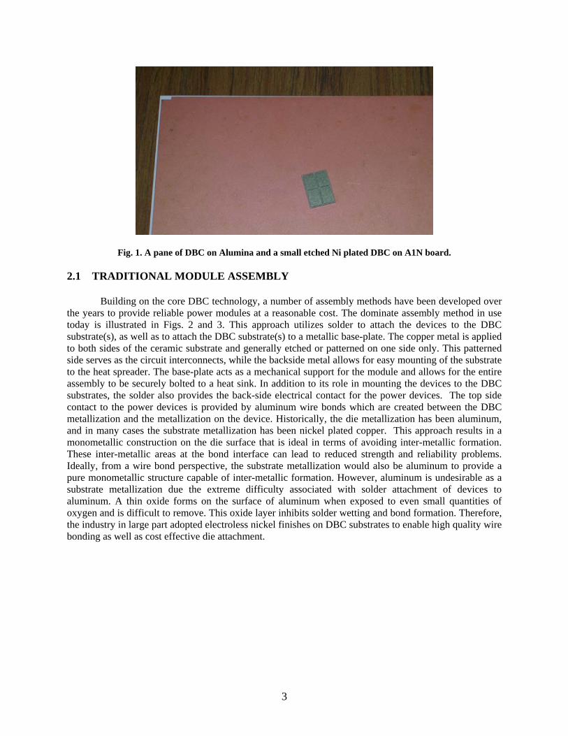
Thick films on ceramic substrates such as Alumina are still used in a number of applications due to the relatively low cost of manufacture and their robust nature in the harsh automotive environment. However, this technology is fundamentally limited by conductors that can readily be fabricated and used to interconnect the devices. Since this technology relies on screen printed traces, the interconnects are limited in thickness to a few mils and are lower in conductivity than pure metals due to their cermet nature. Since high current levels are required in HEV and PHEV power modules, this technology is not ideal for these applications since the efficiencies and therefore the vehicle range would be somewhat diminished in comparison to other packaging technologies. Insulated metal substrates (IMS) are another technology that is commonly used in power electronic systems. These substrates consist of a copper foil bonded to a metal base-plate with the use of a polymer dielectric. As a result, this technology also suffers from the inability to create very thick conductor traces since the copper must be laminated to the metal support plate. In addition, the polymer dielectric greatly limits both the maximum operating temperature of the module as well as the thermal management since this polymer layer is 10–100 times lower in thermal conductivity than commonly available ceramic substrates. While this layer is in fact thin, its impact on thermal performance is significant, and as a result IMS technology is prevalent in relatively low power assemblies (less than 1 kW) rather than in larger traction drives. The most common technology found in high power systems is direct bond copper on ceramic. The basic technology was developed in the 1970s and patented by General Electric (GE) in 1976 [7] and enables thick pure layers of copper to be intimately bonded to high thermal conductivity ceramics. The basic process involves placing the copper foil in direct contact with the ceramic substrate and heating the assembly in a controlled atmosphere. When the oxygen content in the firing furnace is maintained at a low level through the use of nitrogen purge gas and the assembly is heated to 1065°C, a strong eutectic bond forms between the ceramic and the copper. The resulting combination provides for very low loss circuit interconnects capable of withstanding hundreds of amperes of current and a strong stable dielectric layer. Initially, the technology was adopted for use with Alumina substrates where copper was bonded to both sides in order to create a circuit interconnect structure. This technology is now commonly available for use with Alumina, Beryllium Oxide, and Aluminum Nitride (AlN) substrates and has become the foundation for high power modules based on insulated-gate bipolar transistor (IGBTs), metal oxide semiconductor field-effect transistors (MOSFETs), diodes, and similar components commonly utilized in a die rather than a wafer format. As shown in Fig. 1, this material can be obtained in a panel form to be etched or etched to the user’s desired specifications by several vendors. The most popular DBC substrate utilizes copper layers ranging from 0.2–0.4 mm in thickness in conjunction with AlN substrates. AlN is attractive due to the high thermal conductivity and low toxicity of this material in comparison to Alumina and Beryllium Oxide respectively. In addition, the thick conductors combined with high breakdown strength of the material make it a natural choice for many applications [8].
3
Fig. 1. A pane of DBC on Alumina and a small etched Ni plated DBC on A1N board. 2.1 TRADITIONAL MODULE ASSEMBLY
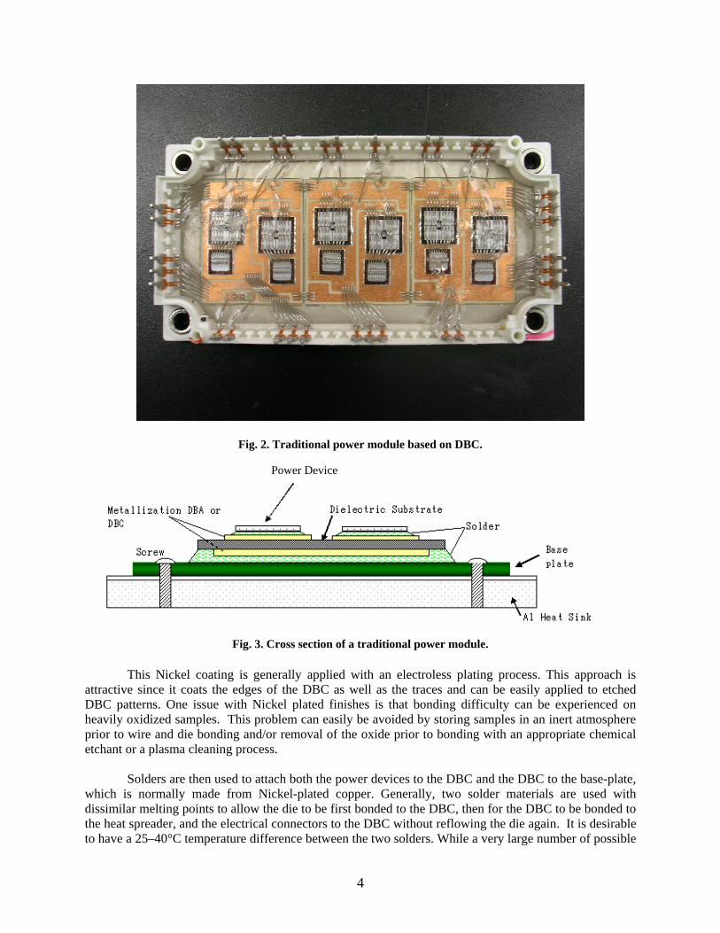
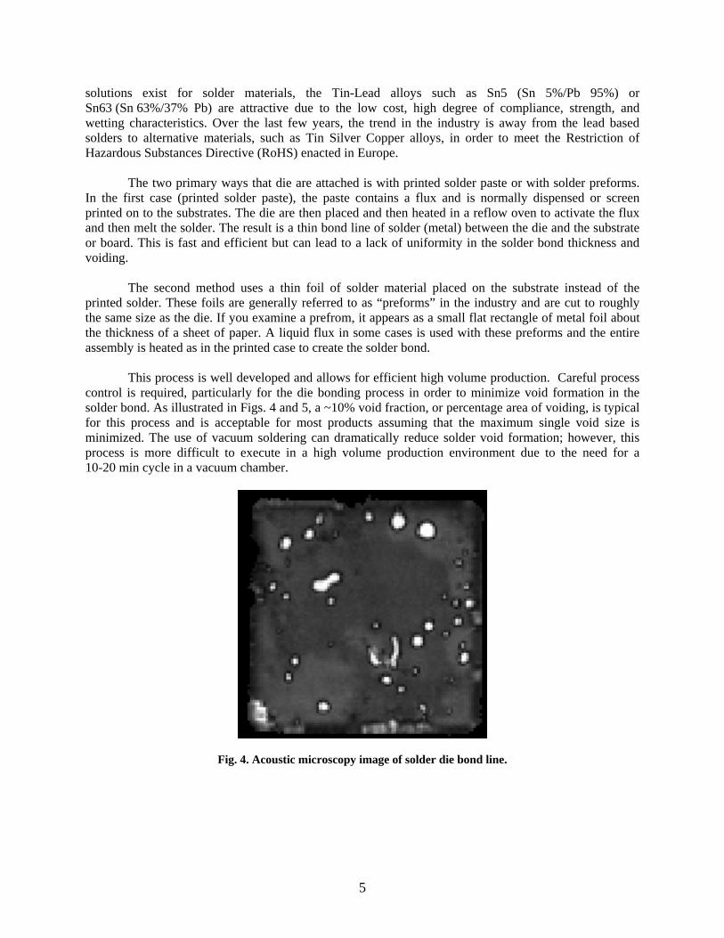
Building on the core DBC technology, a number of assembly methods have been developed over the years to provide reliable power modules at a reasonable cost. The dominate assembly method in use today is illustrated in Figs. 2 and 3. This approach utilizes solder to attach the devices to the DBC substrate(s), as well as to attach the DBC substrate(s) to a metallic base-plate. The copper metal is applied to both sides of the ceramic substrate and generally etched or patterned on one side only. This patterned side serves as the circuit interconnects, while the backside metal allows for easy mounting of the substrate to the heat spreader. The base-plate acts as a mechanical support for the module and allows for the entire assembly to be securely bolted to a heat sink. In addition to its role in mounting the devices to the DBC substrates, the solder also provides the back-side electrical contact for the power devices. The top side contact to the power devices is provided by aluminum wire bonds which are created between the DBC metallization and the metallization on the device. Historically, the die metallization has been aluminum, and in many cases the substrate metallization has been nickel plated copper. This approach results in a monometallic construction on the die surface that is ideal in terms of avoiding inter-metallic formation. These inter-metallic areas at the bond interface can lead to reduced strength and reliability problems. Ideally, from a wire bond perspective, the substrate metallization would also be aluminum to provide a pure monometallic structure capable of inter-metallic formation. However, aluminum is undesirable as a substrate metallization due the extreme difficulty associated with solder attachment of devices to aluminum. A thin oxide forms on the surface of aluminum when exposed to even small quantities of oxygen and is difficult to remove. This oxide layer inhibits solder wetting and bond formation. Therefore, the industry in large part adopted electroless nickel finishes on DBC substrates to enable high quality wire bonding as well as cost effective die attachment.
4
Fig. 2. Traditional power module based on DBC.
Fig. 3. Cross section of a traditional power module. This Nickel coating is generally applied with an electroless plating process. This approach is
attractive since it coats the edges of the DBC as well as the traces and can be easily applied to etched DBC patterns. One issue with Nickel plated finishes is that bonding difficulty can be experienced on heavily oxidized samples. This problem can easily be avoided by storing samples in an inert atmosphere prior to wire and die bonding and/or removal of the oxide prior to bonding with an appropriate chemical etchant or a plasma cleaning process.
Solders are then used to attach both the power devices to the DBC and the DBC to the base-plate,
which is normally made from Nickel-plated copper. Generally, two solder materials are used with dissimilar melting points to allow the die to be first bonded to the DBC, then for the DBC to be bonded to the heat spreader, and the electrical connectors to the DBC without reflowing the die again. It is desirable to have a 25–40°C temperature difference between the two solders. While a very large number of possible
Power Device
5
solutions exist for solder materials, the Tin-Lead alloys such as Sn5 (Sn 5%/Pb 95%) or Sn63 (Sn 63%/37% Pb) are attractive due to the low cost, high degree of compliance, strength, and wetting characteristics. Over the last few years, the trend in the industry is away from the lead based solders to alternative materials, such as Tin Silver Copper alloys, in order to meet the Restriction of Hazardous Substances Directive (RoHS) enacted in Europe.
The two primary ways that die are attached is with printed solder paste or with solder preforms.
In the first case (printed solder paste), the paste contains a flux and is normally dispensed or screen printed on to the substrates. The die are then placed and then heated in a reflow oven to activate the flux and then melt the solder. The result is a thin bond line of solder (metal) between the die and the substrate or board. This is fast and efficient but can lead to a lack of uniformity in the solder bond thickness and voiding.
The second method uses a thin foil of solder material placed on the substrate instead of the printed solder. These foils are generally referred to as “preforms” in the industry and are cut to roughly the same size as the die. If you examine a prefrom, it appears as a small flat rectangle of metal foil about the thickness of a sheet of paper. A liquid flux in some cases is used with these preforms and the entire assembly is heated as in the printed case to create the solder bond.
This process is well developed and allows for efficient high volume production. Careful process
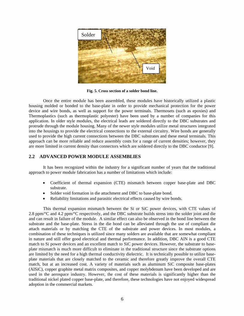
control is required, particularly for the die bonding process in order to minimize void formation in the solder bond. As illustrated in Figs. 4 and 5, a ~10% void fraction, or percentage area of voiding, is typical for this process and is acceptable for most products assuming that the maximum single void size is minimized. The use of vacuum soldering can dramatically reduce solder void formation; however, this process is more difficult to execute in a high volume production environment due to the need for a 10-20 min cycle in a vacuum chamber.
Fig. 4. Acoustic microscopy image of solder die bond line.
6
Void
Solder
Void
Solder
Fig. 5. Cross section of a solder bond line.
Once the entire module has been assembled, these modules have historically utilized a plastic housing molded or bonded to the base-plate in order to provide mechanical protection for the power device and wire bonds, as well as support for the power terminals. Thermosets (such as epoxies) and Thermoplastics (such as thermoplastic polyester) have been used by a number of companies for this application. In older style modules, the electrical leads are soldered directly to the DBC substrates and protrude through the module housing. Many of the newer style modules utilize metal structures integrated into the housings to provide the electrical connections to the external circuitry. Wire bonds are generally used to provide the high current connections between the DBC substrates and these metal terminals. This approach can be more reliable and reduce assembly costs for a range of current densities; however, they are more limited in current density than connectors which are soldered directly to the DBC conductor [9]. 2.2 ADVANCED POWER MODULE ASSEMBLIES It has been recognized within the industry for a significant number of years that the traditional approach to power module fabrication has a number of limitations which include:
• Coefficient of thermal expansion (CTE) mismatch between copper base-plate and DBC substrate.
• Solder void formation in die attachment and DBC to base-plate bond. • Reliability limitations and parasitic electrical effects caused by wire bonds.
This thermal expansion mismatch between the Si or SiC power devices, with CTE values of
2.8 ppm/°C and 4.2 ppm/°C respectively, and the DBC substrate builds stress into the solder joint and die and can result in failure of the module. A similar effect can also be observed in the bond line between the substrate and the base-plate. Stress in the die bond can be alleviated through the use of compliant die attach materials or by matching the CTE of the substrate and power devices. In most modules, a combination of these techniques is utilized since many solders are available that are somewhat compliant in nature and still offer good electrical and thermal performance. In addition, DBC AlN is a good CTE match to Si power devices and an excellent match to SiC power devices. However, the substrate to base-plate mismatch is much more difficult to eliminate in the traditional structure since the substrate options are limited by the need for a high thermal conductivity dielectric. It is technically possible to utilize base-plate materials that are closely matched to the ceramic and therefore greatly improve the overall CTE match, but at an increased cost. A variety of materials such as aluminum SiC composite base-plates (AlSiC), copper graphite metal matrix composites, and copper molybdenum have been developed and are used in the aerospace industry. However, the cost of these materials is significantly higher than the traditional nickel plated copper base-plate, and therefore, these technologies have not enjoyed widespread adoption in the commercial markets.
7
Instead of using alternative base-plate materials, a number of manufacturers have developed
power module assemblies which do away with the base-plate and associated solder interface completely in favor of pressure contacts between the DBC substrate and the heat sink. Packages such as the SEMITOPTM, SKiiPPACKTM, and MiniSKiiPTM are examples of approaches developed by SEMIKRON International [10–13]. The basic idea is to provide uniform pressure over the DBC substrate in a manner that provides a solid contact between the back side of the DBC and a heat sink. Since the heat sink and DBC are not bonded together, they are able to expand and contract separately thereby elevating stress that would otherwise build up due to thermal expansion differences in the two materials. Consistent uniform pressure is required to minimize the thermal resistance of the interface between the heat sink and the DBC substrate. Without this pressure, the thermal resistance would be very large and the power ratings of the modules would require considerable derating to maintain reliable device temperatures. Some risks exist in applying pressure to the DBC directly without a base-plate since the ceramic dielectric is far more fragile than a metal base-plate.
Wire bond failure is another key concern. A recent report illustrated that modules are very
reliable if the junction temperatures are limited to 125°C. However, increasing the junction temperature to 150oC creates a temperature difference between the device junction and the coolant loop (ΔTj) of 85°C. This much larger temperature difference has been shown to lead to wire bond lift-off in only 41,000–42,800 power cycles. At this point, the delamination in the solder joint between the DBC substrate and base-plate was measured to be only 4.6% [2]. Therefore, wire bond lift-off and heel crack formation is a key limiting factor for power modules. The principal problem is the large CTE of the aluminum wire relative to the Si or SiC device. As the module expands and contracts due to thermal deviations in the wire, devices, and substrate, the wires flex and contract in response to these thermal excursions. In contrast, the changes in the devices and substrate are far smaller and the result is stress on the wire bonds. Poorly formed or mechanically damaged bonds may exhibit heel breaks at the location where the wire bends up from the die surface. This mechanical damage may be the result of inappropriate bond parameters, usually too much bonding force and ultrasonic power, or some other physical damage created during assembly or use. These heel cracks may not be visible after the initial assembly, but they grow in response to the stress created during the modules operation and may lead to premature failure of the module. However, for well formed bonds, the principal failure mechanism is wire bond lift-off where the bond comes loose from the die surface and leaves behind a thin layer of aluminum, followed by heel cracks created by CTE mismatches in the module [14]. It has been shown that this process of wire bond lift-off begins by crack formation in the bond weld near the die surface [15]. As the crack propagates, the current density is increased in the surrounding bond area ultimately leading to interruption of the current and lift-off of the wire from the die surface. One possible solution to this problem is the use of molybdenum tabs that are soldered to the die surface. The wire bonds are then formed on the surface of the tabs, which in some cases may be plated with nickel or aluminum. Since the molybdenum has a CTE value (5.1 ppm/°C) that is closer to the aluminum wire (23.8 ppm/°C) than the semiconductor device (2.6 ppm/°C for Si), this metal tab reduces the stress in the wire bonds and improves reliability [16]. This concept has been known to be effective for a very long time and has been used in a variety of high reliability packaging applications for years [17]. More recently this technique has been applied to power modules to improve their overall reliability [18].
Another way in which the industry has worked to eliminate the problems associated with wire
bonds is through the use of novel assembly methods which make connections to both sides of the devices with solder or braze alloys. There are a wide variety of these methods, some of which are based on metal clips or structures [19–24], while other methods are based on ceramic [25–27] or polymeric interconnect structures placed on top of the device [28–32]. All of these methods seek to use alternative methods to make the top side electrical connections without wire bonds. An example of one of these packaging methods that was developed (patent pending) is illustrated in Fig. 6. This particular module was designed

8
for use with spray cooling and combines a 600V IGBT and 600V diode into a single flip-chip assembly which is bonded to a DBC substrate and occupies slightly less space than the normal chip and wire approach. The power devices processed to create a solderable metallization on the top surface of the device and are then bumped with solder as shown in Fig. 6 [33–35]. The die is then flip-chip bonded to DBC and an aluminum nitride heat spreader is used to create the topside electrical contact. This type of approach greatly reduces the inductance of the top side connection and has potential for improved reliability [34].
Flip chip diode & IGBT
Solder Bump
Bumped IGBT
Flip chip diode & IGBT
Solder Bump
Bumped IGBT
Fig. 6. Flip-chip bonded power package designed for liquid spray cooling.
2.3 CURRENT HEV MODULE ASSEMBLIES
Initial electronic components found in HEVs, including the inverters and converters, are based on this traditional module structure. As has been reported and is clearly visible in the images provided in a prior Oak Ridge National Laboratory (ORNL) report† [3], both the Prius converter module and the integrated power electronics module (IPEM) which form the heart of the inverter and boost converter are fabricated with DBC technology. In both cases, IGBTs and power diodes have been bonded to DBC AlN substrates with solder and then wire bonded using heavy aluminum wire bonds. The DBC substrates are soldered to base-plates which are then bolted to coldplates. Water flowing through the cold plates effectively cools the modules. Silicone Gel encapsulation is clearly visible as is commonly used in industry standard modules, such as the one illustrated in Fig. 2. To date, these modules have been able to leverage the traditional technology effectively since the operating temperatures of the module are within the specifications of normal industrial motor drives.
† Figures 5.5, 5.6, 5.7 on pages 53 and 54, as well as Figs. 5.12 and 5.13 on page 57 from Ref. [3).
9
3.0 HIGH TEMPERATURE HEV POWER MODULES
In order to develop modules for HEV applications that can operate at high temperatures, a number of key issues must be addressed in traditional inverter packages. Primarily the issues are:
• The effect of high temperature on the substrate material. • Reliability of the conductor material and its adhesion to the substrate. • Traditional die bonding materials are inadequate for extended use at 200°C. • Wire bonds and bond metallurgy must be carefully considered. • Encapsulation materials must be eliminated or be stable at high operating temperatures.
3.1 SUBSTRATE MATERIALS
In terms of its use for automotive power inverters operating at 200°C, AlN offers several
attractive features, including a close match in CTE to Si and SiC as well as good thermal stability. For this application while operating at these temperatures, most polymeric substrates are not suitable either due to their low glass transition temperatures or their very low thermal conductivities. In contrast, ceramic substrates are viable options at temperatures well above 200°C, and they offer much higher thermal conductivities than any other viable dielectric option. However, it should be noted that the material properties change significantly with respect to temperature. The thermal conductivity of all the commonly used ceramics decrease with increasing temperature, as illustrated in Fig. 7 [36–38]. As can be seen from the graph, AlN substrates offers a thermal conductivity of ~170 W/mK at room temperature, which then decreases to ~150 W/mK with the exact values somewhat dependent on the vendor. While this effect is undesirable, the change is gradual and can be accounted for in a modules thermal design. The CTE of these materials also closely matches Si and SiC devices over a wide temperature, as illustrated in Fig. 8. It is also interesting to note that Dettmer et al. [37] analyzed the effects of high temperature processing on AlN substrates. This analysis involved firing the substrates repeatedly at 850°C and then measuring the thermal conductivity and surface oxide content using secondary ion mass spectrometry (SIMS). This data illustrates that after five temperature excursions to 850°C, the thermal conductivity of the substrates were unchanged and while the top 8 nm of the substrate was slightly oxidized, no degradation of the substrates was observed. In addition, numerous researchers have demonstrated the stability of AlN in conjunction with thick film gold metallizations for applications such as instrumentation of jet engines at 500°C ambient [39]. One can infer from this testing that the AlN substrates are stable for operating temperatures well above those proposed for HEV applications, as well as any assembly operations that a module might be subjected to.
A separate but related question is the ability of the conductor material in combination with the
substrate material to reliably operate at the desired temperatures over the intended product lifetime. For a lower power system, the conductors are normally thin so that the substrate expansion and contraction is dominated by the substrate material itself and not the conductor. For a high power system, a thick highly conductive trace is required so that the module losses are minimized. In addition, a trace that is too thin for the required current density may actually fail due to overheating created by the electrical losses in the conductor. Therefore, since this thick conductor is required and all of the good conductors have high CTE values relative to ceramics and power devices, the stresses in a power substrate are much higher than in a low power substrate. This fact makes the design of power modules more complicated in this respect than low power systems with low current densities. While other options are possible, thick copper layers are ideal due to the high current densities common in the power circuitry. The key issue is the CTE of the copper relative to the ceramic substrate. While no published data on the strength of bare AlN DBC substrates as a function of thermal cycling is available, this data is available for Alumina [40]. The key issue is the thickness of the copper relative to the ceramic, as well as the ceramic strength. In this study,
10
DBC layers thinner than 0.4 mm (16 mils) are capable of withstanding more than 10,000 temperature shock cycles† from -40–110°C without failure. Very thick copper layers lead to fracture of the ceramic substrate and failure after much fewer thermal cycles. This effect can also be observed in published peel strength data for Alumina and Beryillia DBC substrates, where a decrease in peel strength is observed as the copper thickness increases [41]. Similar analysis conducted by one DBC vendor‡ suggests that similar performance is exhibited by AlN DBC. The primary problem with thicker layers tends to be at the lower end of the temperature cycle rather than at the upper end of the cycle. This low temperature failure mechanism can be mitigated by “dimpling” the conductor at the edges of the copper traces. These dimples are simply small holes etched in the top side copper metallization in a regular pattern along the edge of the trace. Dimples effectively reduce the stress at the corners, where the stress is concentrated, and greatly increase the stability of the DBC substrate relative to thermal shock [42]. A recently published report on AlN DBC substrates bonded to AlSiC also confirms this thickness effect; however, it is unclear from this data which solder was used to mount the DBC to the AlSiC base-plate, and what role if any this may play in the reliability of the overall structure [43].
Fig. 7. Thermal conductivity of AlN and BeO vs. temperature.
† Based on an air-to-air thermal shock with a maximum of three second transfer time between -40–110°C and five minutes maximum time for samples to reach temperature extremes. Total cycle time was 35 minutes [40]. ‡ Private communication with Curamik Electronics GmbH.
0
50
100
150
200
250
300
0 50 100 150 200 250 300Temperature (oC)
Ther
mal
Con
duct
ivity
(W
/mk)
AlN (C. K . Unni)AlN (Occhionero 1997)AlN (Bloom 1990)
BeO (Occhionero 1997)BeO (Bloom 1990)
Fit of Average AlN dataFit of Average BeO data

11
Fig. 8. Thermal expansion of common ceramics and device materials vs. temperature [38]. It is also interesting to note that the overall bond strength of the DBC substrate may be impacted
by the soldering process used to bond the die to the substrate or the substrate to a base-plate. Published data clearly indicates that fluxless soldering processes which utilize hydrogen to inhibit oxide formation can dramatically reduce the bond strength between the copper and ceramic layers [41]. For example, forming gas which contains 10% hydrogen and 90% nitrogen and is commonly used in this process, attacks the oxide bond and dramatically weakens the substrate.
An alternative substrate material is direct bond aluminum (DBA) [44]. DBA is very similar to DBC, but the metal layer bonded to the substrate is pure aluminum rather than pure copper. DBA substrates offer slightly lower electrical conductivity and thermal conductivity than DBC substrates; however, published data suggests that DBA substrates may be less prone to delaminating than DBC substrates. This difference is attributed to the aluminum’s lower module of elasticity in comparison to copper, which generates lower levels of stress at the DBA to ceramic interface than for copper in the DBC to ceramic interface. While aluminum is significantly higher in CTE than copper, the DBA is constrained to some degree by the ceramic in much the same way as the DBC is constrained by the ceramic substrate [45]. As a result, the CTE of the DBA substrates is only slightly higher than DBC substrates on equivalent thickness ceramic with equivalent metal thickness. This technology is new and more analysis is needed to explore its potential for high temperature modules. However, it should be noted that selectively plating nickel on DBA substrates would allow solder or braze attachment of power devices to nickel and wire bonding of aluminum wires directly to aluminum.
Another alternative substrate material is silicon nitride (Si3N4) which is now available with DBC
metallization (Kyocera). Little published data is available on these materials; however, the Si3N4 ceramic is stronger than Alumina or aluminum nitride. Since the failures in most DBC substrates is cracking in the ceramic just beneath the DBC layer, the Si3N4 substrates are advertised to be able to better withstand thermal cycling without fracture of the ceramic substrate.
0.000
0.050
0.100
0.150
0.200
0.250
100 150 200 250 300Temperature (oC)
Line
ar T
herm
al E
xpan
sion
(%)
SiC AlNSi BeOAlumina
12
3.2 DIE ATTACHMENT MATERIALS A very wide range of die attachment methods are in use today. Adhesives are unattractive for these applications due to their inferior thermal and electrical conductivity. In addition, it has been shown that while in some cases the bulk thermal conductivities can be improved through the use of filler materials, the interfacial resistance can still be quite high. For power modules, the most common die attach materials are the solder such as the lead tin alloys. These materials offer good electrical and thermal conductivity with a soft compliant nature that absorbs some of the stresses created by CTE differences between the die and substrate. In contrast, hard solders such as high gold content alloys and some braze materials transfer the bulk of the stress to the die and may result in reduced reliability [46]. Many of these soft solders are available with process temperatures well above 200°C and are therefore strong candidates for high temperature die attachment in PHEV and HEV applications. The most likely lead based solders are the high lead content alloys such as 95.5Pb 2Sn 2.5Ag or 95Pb 5Sn. With liquidus temperatures in excess of 300°C, the materials are able to withstand the repeated excursions to high temperatures [47]. Alternative methods are also under development such as lead free solders that conform to the ROHS directive [48], as well as sintered silver die attach methods [49,50]. To date, these methods have not enjoyed wide-spread adoption in the industry, and more analysis is needed to access their suitability for high temperature HEV and PHEV applications. 3.3 WIRE BONDS Two primary issues must be addressed for reliable top side connection to power devices; inter-metallic growth and reliability during power/temperature cycling. The top side device interconnect technology that is used in the power industry today is ultrasonic heavy aluminum wire bonding. Aluminum wire is the dominate technology in this industry since its soft nature allows the use of much larger wires than is normally possible with harder metals [51]. However, aluminum has a low melting point relative to other metals and is susceptible to inter-metallic formation if bonded to inappropriate metals. Also, its large CTE as compared to Si devices and common substrate materials can lead to bond lift-off and module failure. The tendency to form inter-metallic compounds is both a time and temperature dependent phenomenon, and therefore, is exacerbated by operation of the devices at elevated junction temperatures. The most commonly studied form of aluminum inter-metallic is the series of gold aluminum alloys which form when aluminum wire is bonded to gold metallization [52]. This formation is sometimes referred to as the purple plague due to the visible color change created by AuAl2 and leads to bond failure since formation of these alloys creates voids in the bond line and weakens the bond. This process of void formation can occur at temperatures as low as 175°C and in time frames as short as 500 hours. While this gold aluminum inter-metallic problem does not occur in power modules since gold is normally avoided, similar potential problems can occur with other metallization. For example, it has been documented that aluminum and copper can form inter-metallic compounds that also weaken the bond between the copper and aluminum wire [53]. In this case, the presence of air inhibits the growth process through the formation of metallic oxides. However, the system still exhibits reduced strength after aging at high temperatures. Some of the test data illustrates an almost 50% decrease in the pull strengths of these bonds after aging in air for 1000 hours at 200°C [53]. Similar decreases have been measured for aging at 250°C and 300°C. This data shows that initially the bond strength drops within 10 hours of aging, but then levels out with stable bond strengths beyond 400 hours of aging at 300°C. This would indicate that from an inter-metallic point of view, this technology may have some potential for high temperature operation, provided that the initial drop in bond strength can be accounted for in the module design.
13
However, a more reliable although slightly higher cost solution may be the nickel aluminum
system. Nickel has been used in microelectronics for a wide variety of applications, but one of its virtues is the very low rates of diffusion of most materials with respect to nickel. It has been documented that aluminum wires bonded to nickel surfaces exhibit very little change in resistivity (~1%) when aged at temperature as high as 300°C for hundreds of hours [54]. Data also indicates that very minor amounts of diffusion occur between the two materials [55] and minimal amounts of inter-metallic compounds are formed [56]. Destructive pull tests conducted on these samples resulted in wire breaks rather than bond failures indicating that, as desired, the aged Al-Ni bonds are stronger than the Al wire itself. This data suggests that aluminum wire bonds on nickel metallization do not significantly degrade due to inter-metallic formation below 350°C. However, it is also known that plated nickel finishes can become brittle after aging at elevated temperatures; therefore, care must be taken to ensure adequate adhesion between the nickel plating and conductive base copper layer.
One way to eliminate the concerns associated with wire bonds and the intrinsic CTE mismatch
that exists between the conductive bond wires and the power devices, is to eliminate the wire bonds completely. As discussed in Section 2.2 of this report, manufacturers have begun to implement flip-chip and other wire bondless packaging methods, particularly at the low end of the power range. While all the published methods to date have focused on Si devices rather than SiC devices, an opportunity exists to exploit these technologies to enable high temperature power inverters for traction drives in PHEV and HEV vehicles. The key positive attributes of this approach include:
• Ability to use more closely CTE matched structures for top side contacts. • Introduction of lower parasitic inductance and resistance. • The use of high temperature soft solders would potentially allow these packages to operate at
much higher temperatures than traditional chip assembly.
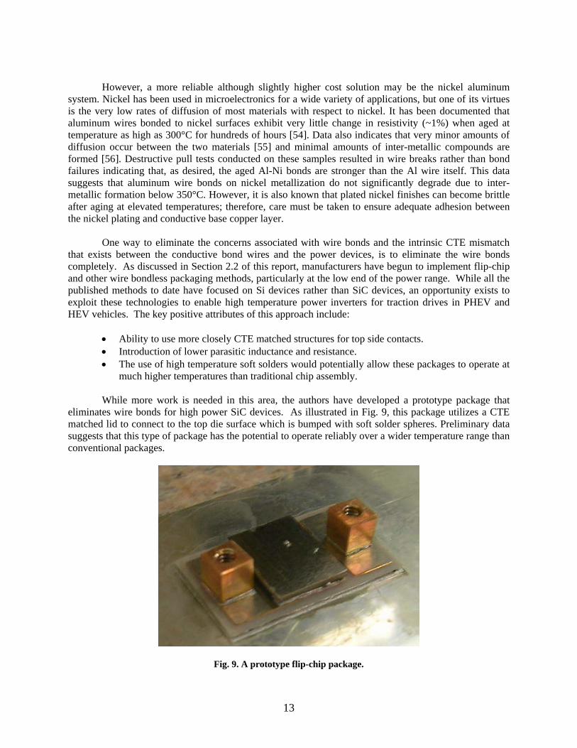
While more work is needed in this area, the authors have developed a prototype package that eliminates wire bonds for high power SiC devices. As illustrated in Fig. 9, this package utilizes a CTE matched lid to connect to the top die surface which is bumped with soft solder spheres. Preliminary data suggests that this type of package has the potential to operate reliably over a wider temperature range than conventional packages.
Fig. 9. A prototype flip-chip package.
14
3.4 ENCAPSULATION
As shown in Fig. 2, conventional modules are encapsulated with a dielectric gel commonly composed of silicone [57–63]. The principal purpose of this gel is to improve the breakdown strength of the package by preventing arcing between the die surface, wire bonds, and adjacent metal features. The material also serves to protect the devices and wire bonds from moisture and contaminants, as well as to aid in reducing mechanical stresses in the devices and bonds. The breakdown voltage of air is approximately 3 kV/mm but is a strong function of humidity. In contrast, the dielectric gels have breakdown values of approximately 18 kV/mm, depending on the exact product. GE makes a number of gels [64] as do several other companies. One of the main functions of the gel is to suppress arcing in the module. If the gel is not used then the air in the module has a much lower break-down voltage and arcing can occur. Humidity further reduces the break-down voltage of air and can create arcing at much lower voltages than would be possible with the use of a gel. The problem for a 200°C junction temperature is that the maximum operating temperature of commercially available gels is 200°C or less. This does not leave an adequate safety margin and may result in arcing inside the package and failure of the inverter. New encapsulates that can operate at higher temperatures are needed to enable existing chip and wire technology to be extended to higher temperatures.
For flip-chip package configurations, surface coatings may be adequate to prevent the electrical
breakdown of these structures. It has been shown that polyimide coatings which are stable at much higher operating temperatures can effectively prevent arcing along the sides of power devices [65]. The adaptation of this approach to flip-chip power packages would enable both high voltage and high temperature operation without the need for improved silicone gels.
15
4.0 SUMMARY & CONCLUSIONS Traditional power modules are based on chip and wire assembly and DBC on ceramic substrates. While this technology can be extended to higher temperatures, the key issues are the substrate material and conductor stability, die bonding material, wire bonds, and bond metallurgy reliability as well as encapsulation materials that are stable at high operating temperatures. Possible solutions to these problems exist in most cases, but require changes to the traditional manufacturing process used in these modules. In addition, a number of emerging technologies such as Si3N4 substrates, flip-chip assembly methods, and the elimination of base-plates would allow reliable module development for operation of HEV and PHEV inverters at elevated junction temperatures.
16
REFERENCES
1. J. M. Miller, “Power Electronics in Hybrid Electric Vehicle Applications,” pp. 23–29 in Eighteenth Annual IEEE Applied Power Electronics Conference and Exposition, APEC’03, 1, February 9–13, 2003.
2. G. Coquery, G. Lefranc, T. Licht, R. Lallemand, N. Seliger, and H. Berg, “High Temperature Reliability on Automotive Power Modules Verified by Power Cycling Tests Up to 150°C,” pp. 1871–1876 in Microelectronics Reliability, 43(9–11), September–November 2003.
3. R. H. Staunton, C. W. Ayers, L. D. Marlino, J. N. Chiasson, and T. A. Burress, Evaluation of 2004 Toyota Prius Hybrid Electric Drive System, ORNL/TM-2006/423, UT-Battelle, LLC, Oak Ridge National Laboratory, Oak Ridge, Tennessee, May 2006.
4. B. Ozpineci, M. S. Chinthavali, L. M. Tolbert, A. Kashyap, and H. A. Mantooth, “A 55 kW Three-Phase Inverter with Si IGBTs and SiC Schottky Diodes,” pp. 541–546 in Twenty-First Annual IEEE Applied Power Electronics Conference and Exposition, APEC’06, March 19–23, 2006.
5. M. S. Chinthavali, B. Ozpineci, and L. M. Tolbert, “High-Temperature and High-Frequency Performance Evaluation of 4H-SiC Unipolar Power Devices,” pp. 322–328 in Twentieth Annual IEEE Applied Power Electronics Conference and Exposition, APEC’05, 1, March 6–10, 2005.
6. B. Ozpineci, L. M. Tolbert, S. K. Islam, and F. Z. Peng, “Testing, Characterization, and Modeling of SiC Diodes for Transportation Applications,” pp. 1673–1678 in IEEE 33rd Annual Power Electronics Specialists Conference, PESC’02, 4, June 23–27, 2002.
7. D. A. Cusano, J. A. Loughran, and Y. S. E. Sun, Direct Bonding of Metals to Ceramics and Metals, United States Patent 3,994,430, November 30, 1976.
8. J. Schulz-Harder and K. Exel, “Advanced DBC Substrates for High Power and High Voltage Electronics,” 11th European Conference on Power Electronics and Applications (EPE), Dresden, Germany, 2005.
9. A. Cosaert, M. Beulque, M. Wolz, O. Schilling, H. Sandmann, R. Spanke, and K. Appelhoff, “Thermal Properties of Power Terminals in High Power IGBT Modules,” Proceedings of the Power Conversion Intelligent Motion Conference, PCIM 1997, Nurnberg, Germany, June 2005.
10. E. Schimanek and G. Mackert, “SKiiPPACK with New Driver Principle ‘OCP’ – The Next Step in Intelligent Power Electronics (OCP – Over Current Protection),” pp. 373–384 in Proceedings of the Power Conversion Intelligent Motion Conference, PCIM 1997, Nurnberg, Germany, June 2005.
11. R. Herzer, R. Popp, B. Koenig, and K. Haeupl, “MiniSKiiP II – Benchmark for 600V CIB Modules,” pp. 297–300 in Proceedings of The 16th International Symposium on Power Semiconductor Devices and ICs, ISPSD’04, May 24–27, 2004.
12. W. Tursky and P. Beckedahl, “Advanced Drive Systems,” pp. 4499–4502 in The 35th Annual IEEE Power Electronics Specialists Conference, Aachen, Germany, 2004.
13. U. Scheuermann, “Reliability of Pressure Contacted Intelligent Integrated Power Modules,” pp. 249–252 in Proceedings of the 14th International Symposium on Power Semiconductor Devices and ICs, June 4–7, 2002.
14. S. Ramminger, N. Seliger, and G. Wachutka, “Reliability Model for Al Wire Bonds Subjected to Heel Crack Failures,” pp. 1521–1525 in Microelectronics Reliability, 40(8–10), August–October 2000.
15. G. Lefranc, B. Weiss, C. Klos, J. Dick, G. Khatibi, and H. Berg, “Aluminum Bond-Wire Properties after 1 Billion Mechanical Cycles,” pp. 1833–1838 in Microelectronics Reliability, 43(9–11), September–November 2003.
16. C. Hager, Y. Tronel, and W. Fichtner, “Electro-Thermo-Mechanical Simulations of Aluminum Bond Wires in IGBT-Packages,” pp. 163–167 in Technical Proceedings of the 1998 International Conference on Modeling and Simulation of Microsystems, 1998.

17
17. D. Palmer and F. Ganyard, “Aluminum Wire to Thick-Film Connections for High-Temperature Operation,” pp. 219–222 in IEEE Transactions on Components, Hybrids, and Manufacturing Technology, 1(3), September 1978.
18. A. Hamidi, S. Kaufmann, and E. Herr, “Increased Lifetime of Wire Bonding Connections for IGBT Power Modules,” pp. 1040–1044 in IEEE Sixteenth Annual Applied Power Electronics Conference and Exposition (APEC 2001), 4, March 4–8, 2001.
19. F. Barlow, “Chip Scale Packaging for Power Devices,” Advancing Microelectronics–Power Electronics Packaging Issue, 28(4), July/August 2001.
20. K. Vanam and F. Barlow, High Power Flip Chip Package, Patent Disclosure No. UAF ID04-30, February 2004.
21. A. Arzumanyan, R. Sodhi, D. Kinzer, H. Schofield, and T. Sammon, “Flip Chip Power MOSFET: A New Wafer Scale Packaging Technique,” pp. 251–254 in Proceedings of the 13th International Symposium on Power Semiconductor Devices and ICs, ISPSD’01, June 4–7, 2001.
22. M. Paulasto-Krockel and T. Hauck, “Flip Chip Die Attach Development for Multichip Mechatronics Power Packages,” pp. 300–306 in IEEE Transactions on Electronics Packaging Manufacturing, 24(4), October 2001.
23. M. Paulasto, T. Hauck, and A. Kolbeck, “Reliability of Flip Chip Die Attach in Multichip Mechatronic Power Module,” pp. 93–100 in Proceedings of the 4th International Conference on Adhesive Joining and Coating Technology in Electronics Manufacturing, June 18–21, 2000.
24. F. Xuejun and S. Haque, “Emerging MOSFET Packaging Technologies and their Thermal Evaluation,” pp. 1102–1108 in The Eighth Intersociety Conference on Thermal and Thermomechanical Phenomena in Electronic Systems, ITHERM 2002, May 30–June 1, 2002.
25. V. Temple, “ ‘Super’ GTO’s Push the Limits of Thyristor Physics,” pp. 604–610 in IEEE 35th Annual Power Electronics Specialists Conference, PESC’04, 1(1), June 20–25, 2004.
26. C. A. Neugebauer, J. F. Burgess, H. J. Glascock, V. A. K. Temple, and D. L. Watrous, “MCT Packaging,” pp. 908–911 in Proceedings of the 40th Electronic Components and Technology Conference, 2, May 20–23, 1990.
27. B. Ozmat, V. A. K. Temple, and J. K. Azotea, “An Advanced Packaging Technology for High Performance Power Devices,” pp. 687–693 in Proceedings of the 32nd Intersociety Energy Conversion Engineering Conference, 1, July 27–August 1, 1997.
28. J. G. Bai, G. Q. Lu, and X. Liu, “Flip-Chip on Flex Integrated Power Electronics Modules for High-Density Power Integration,” pp. 54–59 in IEEE Transactions on Advanced Packaging, 26(1), February 2003.
29. X. Liu, S. Haque, W. J. Wang, and G. Q. Lu, “Packaging of Integrated Power Electronics Modules Using Flip-Chip Technology,” pp. 290–296 in IEEE Fifteenth Annual Applied Power Electronics Conference and Exposition, APEC 2000, 1, February 6–10, 2000.
30. X. Liu, S. Haque, and G. Q. Lu, “Three-Dimensional Flip-Chip on Flex Packaging for Power Electronics Applications,” pp. 1–9 in IEEE Transactions on Advanced Packaging, 24(1), February 2001.
31. H. N. Shah, Y. Xiao, T. P. Chow, R. J. Gutmann, E. R. Olson, S. -H. Park, W. -K. Lee, J. J. Connors, T. M. Jahns, and R. D. Lorenz, “Power Electronics Modules for Inverter Applications Using Flip-Chip on Flex-Circuit Technology,” pp. 1526–1533 in Conference Record of the 2004 IEEE Industry Applications Conference and 39th IAS Annual Meeting, 3, October 3–7, 2004.
32. Y. Xiao, H. N. Shah, R. Natarajan, E. J. Rymaszewski, T. P. Chow, and R. J. Gutmann, “Integrated Flip-Chip Flex-Circuit Packaging for Power Electronics Applications,” pp. 515–522 in IEEE Transactions on Power Electronics, 19(2), March 2004.
33. S. Jittinorasett, F. Barlow, J. McGrath, and A. Elshabini, “UBM Formation on Single Die/Dice for Flip Chip Applications,” pp. 39–44 in Proceedings of the International Conference on Microelectronics Packaging, IMAPS, 1999.
18
34. J. C. Balda, F. D. Barlow, P. Selvam, and A. Elshabini, Direct Cooling of Propulsion Drives for High Power Density and Low Volume, Final Project Report, ONR Award No. N00014-01-1-0634, March 2005.
35. R. Joshi, M. Rios, C. Tangpuz, and E. V. Cruz, “Implementation of Pb-free Bumping in Power Packaging,” pp. 81–84 in 28th International Electronics Manufacturing Technology Symposium, IEMT 2003, IEEE/CPMT/SEMI, July 16–18, 2003.
36. M. A. Occhionero, R.W. Adams, and K. P. Fennessy, “A New Substrate for Electronic Packaging: Aluminum Silicon Carbide (AlSiC) Composites,” pp. 398–403 in Proceedings of the Forth Annual Portable by Design Conference, Electronics Design, March 24–27, 1997.
37. E. S. Dettmer, B. M. Romenesko, H. K. Charles, Jr., B. G. Carkhuff, and D. J. Merrill, “Steady-State Thermal Conductivity Measurements of AlN and SiC Substrate Materials,” pp. 543–547 in IEEE Transactions on Components, Hybrids, and Manufacturing Technology, 12(4), December 1989.
38. T. R. Bloom, “The Reliability of AlN Power Hybrids Using Cu Thick Film Conductive,” pp. 111–115 in Proceedings of the 40th Electronic Components and Technology Conference, 1, May 20–23, 1990.
39. G. W. Hunter, P. G. Neudeck, R. S. Okojie, G. M. Beheim, J. A. Powell, and L. Chen, “An Overview of High-Temperature Electronics and Sensor Development at NASA Glenn Research Center,” pp. 658–664 in Transactions of the ASME, 125, October 2003.
40. W. Martin, B. Waibel, and W. Laaser, “Thermal Resistance and Temperature Cycling Endurance of DBC Substrates,” pp. 29–33 in Hybrid Circuits: Journal of the International Society for Hybrid Microelectronics-UK, May 1990.
41. K. H. Dalal and J. F. Dickson, “Design Trade-Offs and Reliability of Power Circuit Substrates with Respect to Varying Geometrical Parameters of Direct Copper Bonded Al2O3 and BeO,” pp. 923–929 in Industry Applications Conference and Thirtieth IAS Annual Meeting, IAS’95, 1, October 8–12, 1995.
42. J. Schulz-Harder, “Advantages and New Development of Direct Bonded Copper Substrates,” pp. 359–365 in Microelectronics Reliability, 43(3), March 2003.
43. L. Dupont, Z. Khatir, S. Lefebvre, and S. Bontemps, “Effects of Metallization Thickness of Ceramic Substrates on the Reliability of Power Assemblies Under High Temperature Cycling,” pp. 1766–1771 in Microelectronics and Reliability, 46(9–11), September–November 2006.
44. A. Lindemann and G. Strauch, “Properties of Direct Aluminum Bonded Substrates for Power Semiconductor Components,” pp. 4171–4177 in IEEE 35th Annual Power Electronics Specialists Conference, Aachen, Germany, 2004.
45. T. Evans, “Pure Copper Metallization Technologies,” Chapter 5 in Hybrid Microelectronics Handbook, edited by J. Sergent and C. A. Harper, McGraw Hill, 1995.
46. K. Meyyappan, P. McCluskey, and L. Y. Chen, “Thermomechanical Analysis of Gold-Based SiC Die-Attach Assembly,” pp. 152–158 in IEEE Transactions on Device and Materials Reliability, 3(4), December 2003.
47. F. P. McCluskey, M. Dash, Z. Wang, and D. Huff, “Reliability of High Temperature Solder Alternatives,” pp. 1910–1914 in Microelectronics and Reliability, 46(9–11), September–November 2006.
48. D. Huff, D. Katsis, K. Stinson-Bagby, T. Thacker, G. -Q. Lu, and J. D. van Wyk, “Reliability and Microstructure of Lead-Free Solder Die Attach Interface in Si Power Devices,” pp. 567–568 in IEEE Proceedings of the 42nd Annual International Reliability Physics Symposium, April 25–29, 2004.
49. Z. Zhang and G. Q. Lu, “Pressure-Assisted Low-Temperature Sintering of Silver Paste as an Alternative Die-Attach Solution to Solder Reflow,” pp. 279–283 in IEEE Transactions on Electronics Packaging Manufacturing, 25(4), October 2002.
50. G. Q. Lu, J. N. Calata, Z. Zhang, and J. G. Bai, “A Lead-Free, Low-Temperature Sintering Die-Attach Technique for High-Performance and High-Temperature Packaging,” pp. 42–46 in Proceedings of the Sixth IEEE CPMT Conference on High Density Microsystem Design and Packaging and Component Failure Analysis, HDP’04, June 30–July 3, 2004.
19
51. H. M. Ho, W. Lam, S. Stoukatch, P. Ratchev, C. J. Vath, III, and E. Beyne, “Direct Gold and Copper Wires Bonding on Copper,” pp. 913–923 in Microelectronics Reliability, 43(6), June 2003.
52. G. Harman, Wire Bonding in Microelectronics: Materials, Processes, Reliability, and Yield, Second Edition, McGraw-Hill Professional, June 1, 1997.
53. D. Olsen and K. James, “Effects of Ambient Atmosphere on Aluminum — Copper Wirebond Reliability,” pp. 357–362 in IEEE Transactions on Hybrids and Manufacturing Technology, 7(4), December 1984.
54. D. Palmer, “Hybrid Microcircuitry for 300°C Operation,” pp. 252–257 in IEEE Transactions on Parts, Hybrids, and Packaging, 13(3), September 1977.
55. J. T. Benoit, S. Chin, R. R. Grzybowski, L. Shun-Tien, R. Jain, P. McCluskey, and T. Bloom, “Wire Bond Metallurgy for High Temperature Electronics,” pp. 109–113 in High Temperature Electronics Fourth International Conference, HITEC’98, June 14–18, 1998.
56. J. T. Benoit, R. R. Grzybowski, and D. B. Kerwin, “Evaluation of Aluminum Wire Bonds for High Temperature (2WC) Electronic Packaging,” pp. III-17–23 in Transactions of the Third International High Temperature Electronics Conference, 1, 1996.
57. D. Frey, J. L. Schanen, J. L. Auge, and O. Lesaint, “Electric Field Investigation in IGBT Power Modules,” pp. 864–867 in Proceedings of the 2004 IEEE International Conference on Solid Dielectrics, ICSD 2004, 2, July 5–9, 2004.
58. D. Frey, J. L. Schanen, J. L. Auge, and O. Lesaint, “Electric Field Investigation in High Voltage Power Modules Using Finite Element Simulations and Partial Discharge Measurements,” pp. 1000–1005 in Conference Record of the 38th IAS Annual Meeting in Industry Applications, 2, October 12–16, 2003.
59. J. L. Auge, O. Lesaint, D. Frey, and J. L. Schanen, “Optical and Electrical Investigation of Dielectric Gel Behavior Under High Electrical Field,” pp. 912–915 in Proceedings of the 2004 IEEE International Conference on Solid Dielectrics, ICSD 2004, 2, July 5–9, 2004.
60. F. Breit, D. Malec, and T. Lebey, “Investigations on DC Conductivity and Space Charge in Silicone Gel,” pp. 48–51 in Annual Report Conference on Electrical Insulation and Dielectric Phenomena, October 20–24, 2002.
61. M. T. Do, J. -L. Auge, and O. Lesaint, “Optical Measurement of Partial Discharges in Silicone Gel Under Repetitive Pulse Voltage,” pp. 360–363 in Proceedings of 2005 International Symposium on Electrical Insulating Materials, ISEIM 2005, 2, June 5–9, 2005.
62. G. Mitic and G. Lefranc, “Localization of Electrical-Insulation- and Partial-Discharge Failures of IGBT Modules,” pp. 1453–1458 in Conference Record of the 1999 IEEE Industry Applications Conference and Thirty-Fourth IAS Annual Meeting, 2, October 3–7, 1999.
63. T. Lebey, D. Malec, V. Bley, F. Breit, and E. Dutarde, “Contribution to the Dimensioning of the Different Insulating Materials Used in High Voltage Power Electronics Module Manufacturing,” pp. 55–59 in The Fifth International Conference on Power Electronics and Drive Systems, PEDS 2003, 1, November 17–20, 2003.
64. General Electric Company, GE Advanced Materials–Silicones, http://www.gefluids.com/gesilicones/ 65. G. Mitic, T. Licht, and G. Lefranc, “IGBT Module Technology with High Partial Discharge
Resistance,” pp. 1899–1904 in Conference Record of the 2001 IEEE Industry Applications Conference and Thirty-Sixth IAS Annual Meeting, 3, September 30–October 4, 2001.
20
DISTRIBUTION
Internal
1. D. J. Adams 2. M. S. Chinthavali 3. K. P. Gambrell 4. E. C. Fox 5. L. D. Marlino
6. M. Olszewski 7. B. Ozpineci 8. L. M. Tolbert 9. Laboratory Records
External
10. R. Al-Attar, DCX, [email protected]. 11. F. D. Barlow, University of Idaho, Department of Electrical & Computer Engineering, Buchanan
Engineering Laboratory, Rm. 211, 607 Urquhart Avenue, Moscow, Idaho 83844-1023 12. T. Q. Duong, U.S. Department of Energy, EE-2G/Forrestal Building, 1000 Independence Avenue,
S.W., Washington, D.C. 20585. 13. A. Elshabini, University of Idaho, Department of Electrical & Computer Engineering, Buchanan
Engineering Laboratory, Rm. 211, 607 Urquhart Avenue, Moscow, Idaho 83844-1023 14. R. R. Fessler, BIZTEK Consulting, Inc., 820 Roslyn Place, Evanston, Illinois 60201-1724. 15. K. Fiegenschuh, Ford Motor Company, Scientific Research Laboratory, 2101 Village Road, MD-
2247, Dearborn, Michigan 48121. 16. V. Garg, Ford Motor Company, 15050 Commerce Drive, North, Dearborn, Michigan 48120-1261. 17. G. Hagey, Sentech, Inc., 501 Randolph St., Williamsburg, Virginia 23185. 18. E. Jih, Ford Motor Company, Scientific Research Laboratory, 2101 Village Road, MD-1170, Rm.
2331, Dearborn, Michigan 48121. 19. K. J. Kelly, National Renewable Energy Laboratory, 1617 Cole Boulevard, Golden, Colorado
80401. 20. A. Lee, Daimler Chrysler, CIMS 484-08-06, 800 Chrysler Drive, Auburn Hills, Michigan 48326-
2757. 21. F. Liang, Ford Motor Company, Scientific Research Laboratory, 2101 Village Road, MD1170, Rm.
2331/SRL, Dearborn, Michigan 48121. 22. M. W. Lloyd, Energetics, Inc., 7164 Columbia Gateway Drive, Columbia, Maryland 21046. 23. M. Mehall, Ford Motor Company, Scientific Research Laboratory, 2101 Village Road, MD-2247,
Rm. 3317, Dearborn, Michigan 48124-2053. 24. N. Olds, United States Council for Automotive Research (USCAR), [email protected] 25. J. Rogers, Chemical and Environmental Sciences Laboratory, GM R&D Center, 30500 Mound
Road, Warren, Michigan 48090-9055. 26. S. A. Rogers, U.S. Department of Energy, EE-2G/Forrestal Building, 1000 Independence Avenue,
S.W., Washington, D.C. 20585. 27. G. S. Smith, General Motors Advanced Technology Center, 3050 Lomita Boulevard, Torrance,
California 90505. 28. E. J. Wall, U.S. Department of Energy, EE-2G/Forrestal Building, 1000 Independence Avenue,
S.W., Washington, D.C. 20585. 29. B. Welchko, General Motors Advanced Technology Center, 3050 Lomita Boulevard, Torrance,
California 90505. 30. P. G. Yoshida, U.S. Department of Energy, EE-2G/Forrestal Building, 1000 Independence Avenue,
S.W., Washington, D.C. 20585.