high-resolution x-ray diffraction of epitaxial thin-films ... · pdf file•high-resolution...
TRANSCRIPT
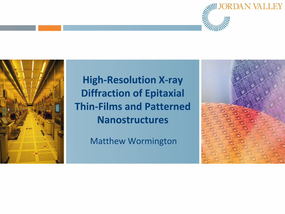
Matthew Wormington
High-Resolution X-ray Diffraction of Epitaxial
Thin-Films and Patterned Nanostructures

2 Frontiers of Characterization and Metrology for Nanoelectronics 2015
Acknowledgements
• Colleagues • Paul Ryan & John Wall (JV UK)
• Kevin Matney & Peter Gin (JV US)
• Isaac Mazor, David Berman, Alex Krokhmal, Yuri Vinshtein & Alex Tokar (JV ILS)
• Collaborators • PY Hung (SEMATECH)
• Manasa Medikonda & Alain Diebold (CNSE)
• Jody Fronheiser & Vimal Kamineni (GlobalFoundries)
• Benoit Lherron (IBM/ST)
• Evguenia Karapetrova (APS)
• Andreas Schulze, Hilde Tielens, Andriy Hikavyy, Roger Loo, Matty Caymax (IMEC)
April 14, 2015
3 Frontiers of Characterization and Metrology for Nanoelectronics 2015
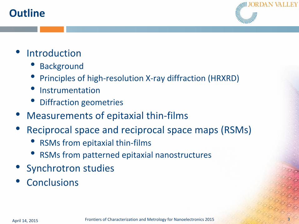
Outline
• Introduction • Background
• Principles of high-resolution X-ray diffraction (HRXRD)
• Instrumentation
• Diffraction geometries
• Measurements of epitaxial thin-films
• Reciprocal space and reciprocal space maps (RSMs) • RSMs from epitaxial thin-films
• RSMs from patterned epitaxial nanostructures
• Synchrotron studies
• Conclusions
April 14, 2015
4 Frontiers of Characterization and Metrology for Nanoelectronics 2015
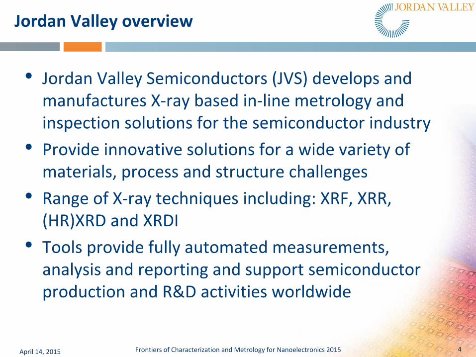
Jordan Valley overview
• Jordan Valley Semiconductors (JVS) develops and manufactures X-ray based in-line metrology and inspection solutions for the semiconductor industry
• Provide innovative solutions for a wide variety of materials, process and structure challenges
• Range of X-ray techniques including: XRF, XRR, (HR)XRD and XRDI
• Tools provide fully automated measurements, analysis and reporting and support semiconductor production and R&D activities worldwide
April 14, 2015

5 Frontiers of Characterization and Metrology for Nanoelectronics 2015
Jordan Valley overview (cont.)
• Private company
• Established 1982, HQ in Israel
• Global presence
• > 180 employees
• Manufacturing and demo sites (Israel & UK)
• Local sales & support offices in strategic locations (US, Taiwan, Korea, Singapore, Europe)
April 14, 2015

6 Frontiers of Characterization and Metrology for Nanoelectronics 2015
• Tools: JVX7300 series
• Channels: XRF, XRR and HRXRD Applications: o 7300HR: SiGe & Si:C on bulk or
(FD)SOI, various ALD films, HKMG stacks, silicides…
o 7300LSI: Ge and III/V on Si for sub-10 nm, HKMG, FinFETs, GaN-on-Si, MEMS
o 7300F(R): Metal / magnetic films, WLP
o 7300G: Ultra-thin films and 3D devices
• In-line tools for silicon semiconductor device manufacturers for process control of product wafers
Silicon semiconductor metrology tools
April 14, 2015
JVX7300LSI

7 Frontiers of Characterization and Metrology for Nanoelectronics 2015
What can HRXRD give us, who uses it and for what?
• High-resolution X-ray diffraction (HRXRD) provides a wealth of information about epitaxial materials • Crystal lattice misfit/strain, tilt and defectivity/quality… • Composition and thickness of planar films • Shape and lattice distortion in patterned structures
• It is first-principles (no calibration) and non-destructive characterization and metrology technique • Does not require material/process dependent optical
constants • Accurate and precise with very few assumptions
• Has been used for 30+ years in the compound semiconductor industry for a wide range of materials (III-V, III-nitride, II-VI…) and devices (LEDs, lasers, CPV, detectors…)

8 Frontiers of Characterization and Metrology for Nanoelectronics 2015
What can HRXRD give us, who uses it and for what (cont.)?
• Introduced into the Si industry with strain engineering for sub-100 nm logic devices • Epitaxial SiGe S/D stressors for
PMOS mobility enhancement • Also Si:C / Si:P S/D stressors for
NMOS, but less widespread
• Used for R&D, CVD chamber qual., process diagnostics / ramp and in-line metrology
• Solid metrology pads less relevant / not available • Transition from planar to 3D
(FinFET) devices • Novel channel materials,
e.g. SiGe, Ge and III-V for sub 10 nm nodes
April 14, 2015
Source: A. Steegen, “Logic Scaling Beyond 10 nm”, IMEC Technology Forum US (July 2013)
9 Frontiers of Characterization and Metrology for Nanoelectronics 2015
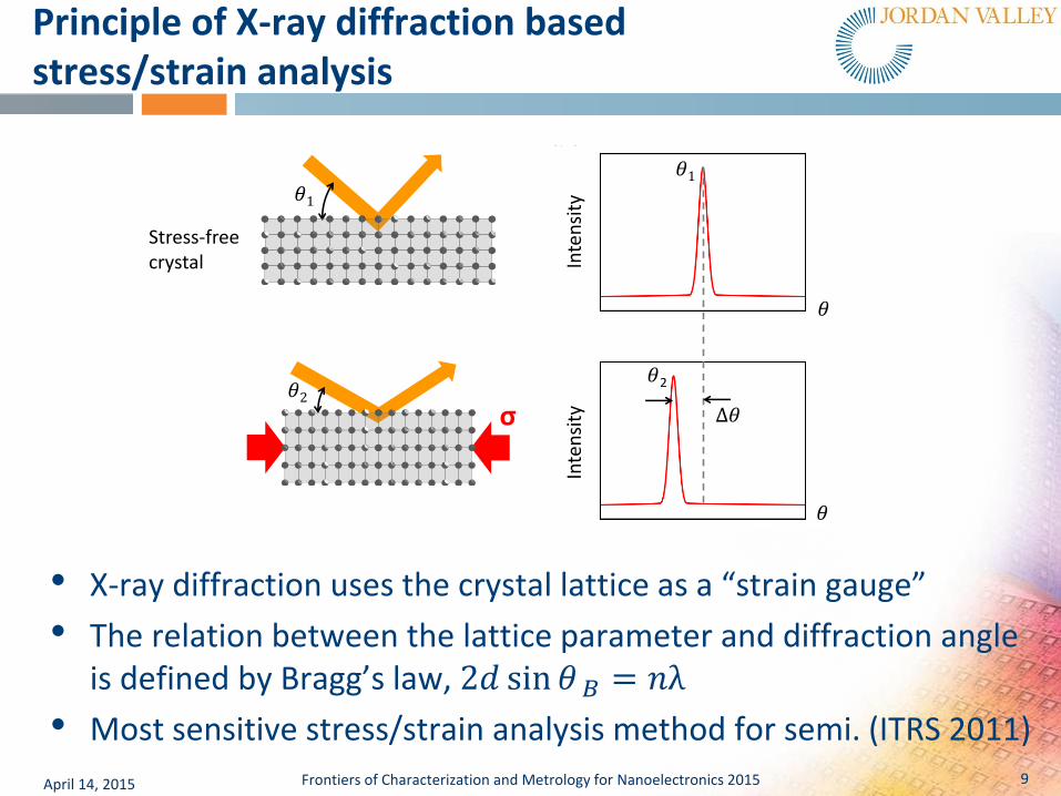
Principle of X-ray diffraction based stress/strain analysis
April 14, 2015
• X-ray diffraction uses the crystal lattice as a “strain gauge”
• The relation between the lattice parameter and diffraction angle is defined by Bragg’s law, 2𝑑 sin 𝜃 𝐵 = 𝑛λ
• Most sensitive stress/strain analysis method for semi. (ITRS 2011)
σ
(a) (b)
(c) (d)
Inte
nsi
tyIn
ten
sity
2
Stress-free crystal
10 Frontiers of Characterization and Metrology for Nanoelectronics 2015
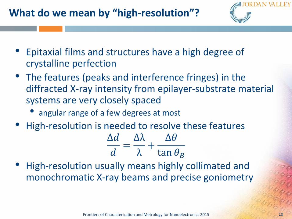
What do we mean by “high-resolution”?
• Epitaxial films and structures have a high degree of crystalline perfection
• The features (peaks and interference fringes) in the diffracted X-ray intensity from epilayer-substrate material systems are very closely spaced • angular range of a few degrees at most
• High-resolution is needed to resolve these features ∆𝑑
𝑑=∆λ
λ+
∆𝜃
tan 𝜃𝐵
• High-resolution usually means highly collimated and monochromatic X-ray beams and precise goniometry
11 Frontiers of Characterization and Metrology for Nanoelectronics 2015
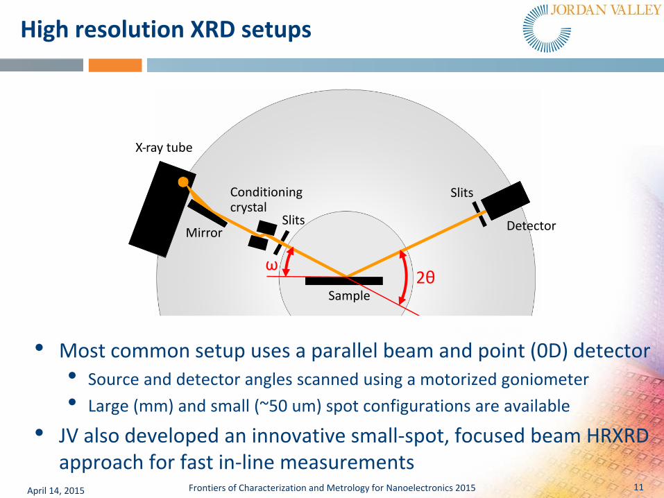
High resolution XRD setups
April 14, 2015
X-ray tube
Conditioningcrystal
Slits
Sample
Mirror
Slits
Detector
2θω
(a)
• Most common setup uses a parallel beam and point (0D) detector • Source and detector angles scanned using a motorized goniometer
• Large (mm) and small (~50 um) spot configurations are available
• JV also developed an innovative small-spot, focused beam HRXRD approach for fast in-line measurements

12 Frontiers of Characterization and Metrology for Nanoelectronics 2015
Common Bragg diffraction geometries and anatomy of a HRXRD curve
April 14, 2015
Symmetric geometry
Asymmetric geometries
Glancingincidence
Glancingexit
(a) (b)
10
110
210
310
410
510
610
-2.0 -1.5 -1.0 -0.5 0.0 0.5 1.0In
ten
sity
(arb
. un
its)
ω (deg)
Δω
Substrate peak
Layer peak
Fringes
• Symmetric Bragg geometry is sensitive to lattice parameter perpendicular to the surface
• Asymmetric geometries are also sensitive to the lattice parameters both parallel and perpendicular to the surface

13 Frontiers of Characterization and Metrology for Nanoelectronics 2015
Example: Fully strained SiGe epilayer
April 14, 2015
Symmetric 004 reflection from 22.5 nm epitaxial film of Si1-xGex with x = 49% on a Si(001) substrate
• Composition / strain determined from measured lattice misfit
• Misfit normal to surface from layer peak position
∆𝑑/𝑑 = −∆𝜔 cot θ𝐵
• Thickness from interference fringe period
𝑡 = λ/(2∆𝜔𝑓 cos θ𝐵)
• No dependence on uncertain materials parameters
Measurement Simulation
14 Frontiers of Characterization and Metrology for Nanoelectronics 2015
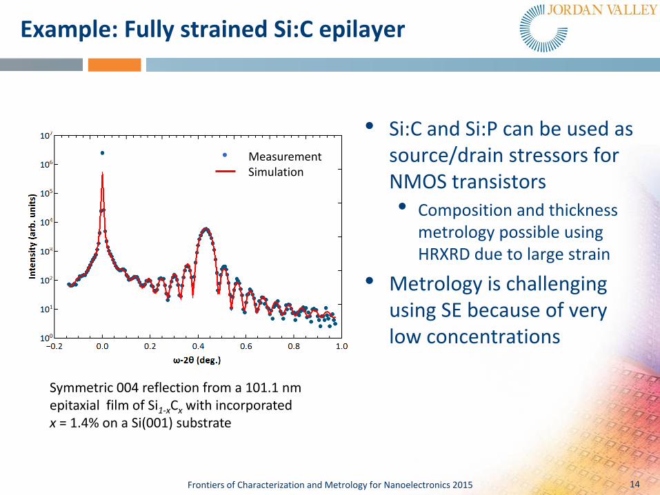
Example: Fully strained Si:C epilayer
• Si:C and Si:P can be used as source/drain stressors for NMOS transistors • Composition and thickness
metrology possible using HRXRD due to large strain
• Metrology is challenging using SE because of very low concentrations
Symmetric 004 reflection from a 101.1 nm epitaxial film of Si1-xCx with incorporated x = 1.4% on a Si(001) substrate
Measurement Simulation

15 Frontiers of Characterization and Metrology for Nanoelectronics 2015
More complex SiGe/Si examples
• More complex stacks give rise to more complex interference effects
• Measured data can be automatically fit to dynamical X-ray diffraction theory by refining the parameters of a structural model
April 14, 2015
Periodic superlattice structure: [8.2nm Si0.9Ge0.1/ 22.4nm Si]×5 on a Si(001) substrate
NIST SRM2000 standard: 23.7nm Si/ 48.2nm Si0.84Ge0.16 on Si(001)
16 Frontiers of Characterization and Metrology for Nanoelectronics 2015
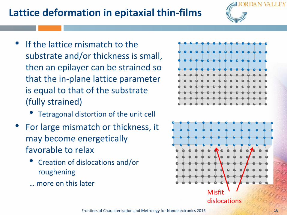
Lattice deformation in epitaxial thin-films
• If the lattice mismatch to the substrate and/or thickness is small, then an epilayer can be strained so that the in-plane lattice parameter is equal to that of the substrate (fully strained) • Tetragonal distortion of the unit cell
• For large mismatch or thickness, it may become energetically favorable to relax • Creation of dislocations and/or
roughening
… more on this later Misfit dislocations

17 Frontiers of Characterization and Metrology for Nanoelectronics 2015
Comparison of HRXRD data from strained and relaxed SiGe epilayers
0 10
1 10
2 10
3 10
4 10
5 10
-7000 -6000 -5000 -4000 -3000 -2000 -1000 0 1000
Inte
nsi
ty (
cps)
OMEGA-2THETA (arcsec)
Partially relaxed layer
t ~ 350 Å (XRR), x > 50%
No interference fringes
“Triangular” layer peak
0 10
1 10
2 10
3 10
4 10
5 10
-3000 -2500 -2000 -1500 -1000 -500 0 500 1000
Inte
nsi
ty (
cps)
Omega (sec)
Fully strained layer
t = 492 Å, x = 19.6%
Interference fringes
• Degradation of device performance and yield loss • Relaxed material has about
50% less strain than a pseudomorphic layer
• Relaxed material will contain dislocations at the interface and in the layer - increased leakage?
• HRXRD provides a unique, automated solution for strain metrology and assessment of lattice defectivity
No interference fringes “Triangular” layer peak
18 Frontiers of Characterization and Metrology for Nanoelectronics 2015
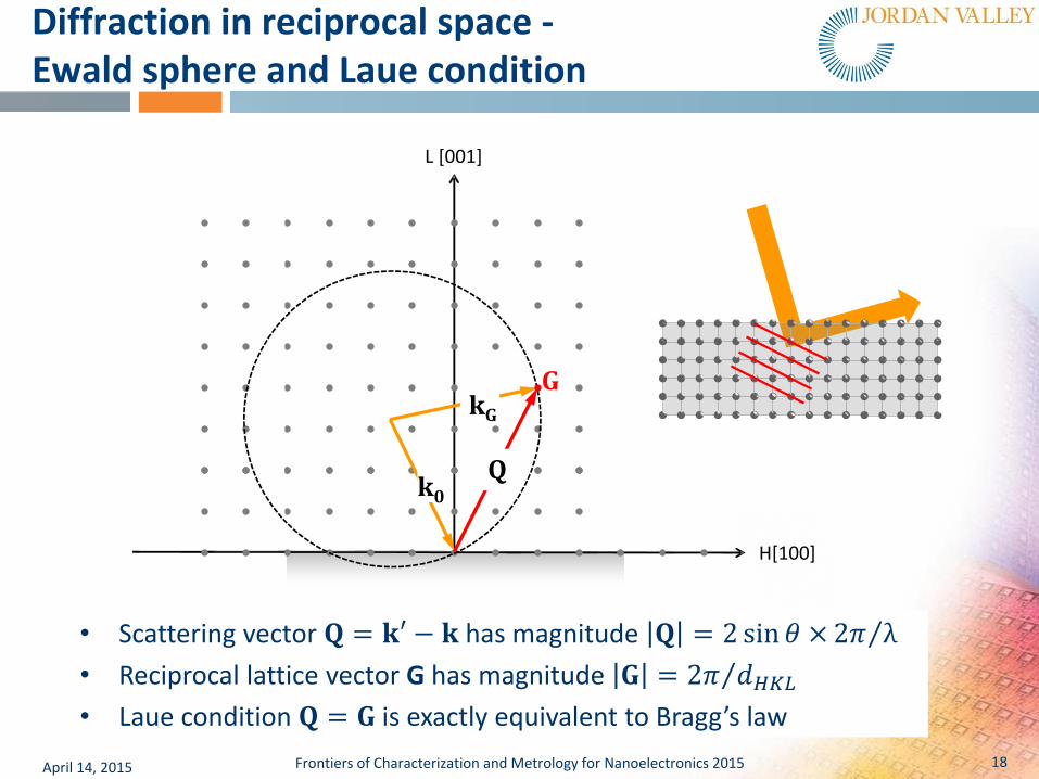
Diffraction in reciprocal space - Ewald sphere and Laue condition
April 14, 2015
H[100]
L [001]
kG
Qk0
(a) (b)
• Scattering vector 𝐐 = 𝐤′ − 𝐤 has magnitude 𝐐 = 2 sin 𝜃 ×2𝜋 λ
• Reciprocal lattice vector G has magnitude 𝐆 = 2𝜋 𝑑𝐻𝐾𝐿
• Laue condition 𝐐 = 𝐆 is exactly equivalent to Bragg’s law

19 Frontiers of Characterization and Metrology for Nanoelectronics 2015
Fast reciprocal space mapping - FastRSMs
• Linear (1D) detector replaces analyzer crystal / slits and point (0D) detector and allows routine RSMs to be measured in the fab
• Simultaneously intensity acquisition over a large range of 2θ angles
• x10-100 faster than conventional approach (minutes not hours)
• Provides more information than available by single HRXRD curves
• Automated RSM analysis for epi. process development and control of thin-films and patterned nanostructures
X-ray tube
Conditioningcrystal
Slits
Sample
Mirror Linear detector
20 Frontiers of Characterization and Metrology for Nanoelectronics 2015
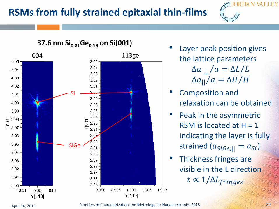
RSMs from fully strained epitaxial thin-films
April 14, 2015
• Layer peak position gives the lattice parameters
∆𝑎 𝑎 = ∆𝐿 𝐿 ∆𝑎|| 𝑎 = ∆𝐻 𝐻
• Composition and relaxation can be obtained
• Peak in the asymmetric RSM is located at H = 1 indicating the layer is fully strained (𝑎𝑆𝑖𝐺𝑒,|| = 𝑎𝑆𝑖)
• Thickness fringes are visible in the L direction 𝑡 ∝ 1/∆𝐿𝑓𝑟𝑖𝑛𝑔𝑒𝑠
004 113ge
37.6 nm Si0.81Ge0.19 on Si(001)
Si
SiGe
21 Frontiers of Characterization and Metrology for Nanoelectronics 2015
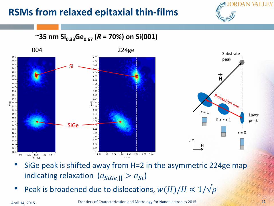
RSMs from relaxed epitaxial thin-films
April 14, 2015
• SiGe peak is shifted away from H=2 in the asymmetric 224ge map indicating relaxation (𝑎𝑆𝑖𝐺𝑒,|| > 𝑎𝑆𝑖)
• Peak is broadened due to dislocations, 𝑤(𝐻)/𝐻 ∝ 1/√𝜌
004 224ge Substratepeak
Layerpeak
r = 1
r = 0
0 < r < 1
H
LH
~35 nm Si0.33Ge0.67 (R = 70%) on Si(001)
Si
SiGe
22 Frontiers of Characterization and Metrology for Nanoelectronics 2015
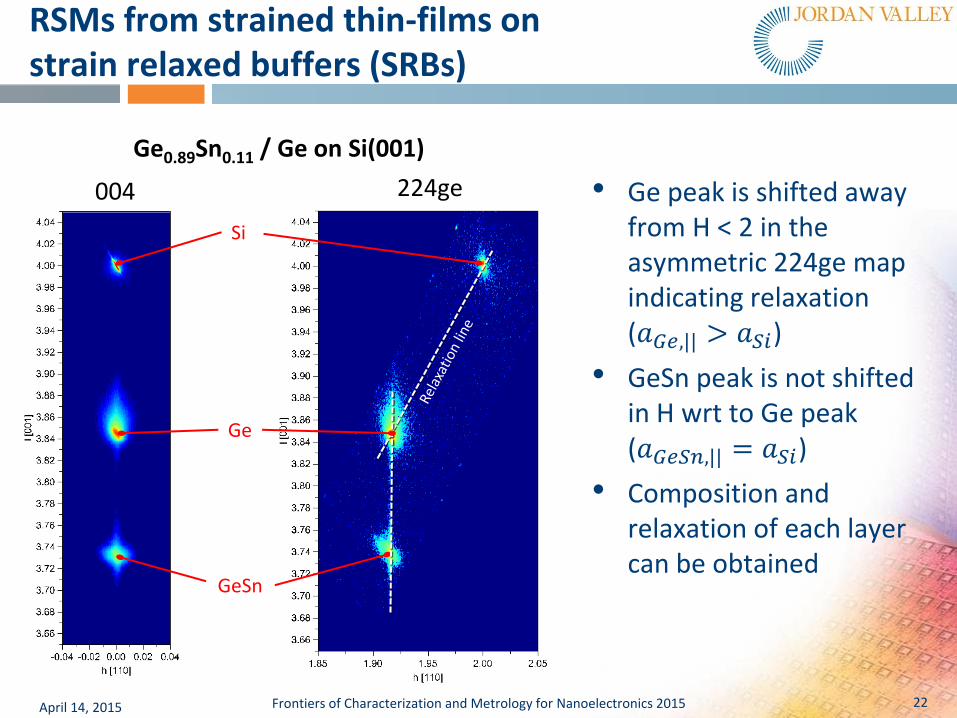
RSMs from strained thin-films on strain relaxed buffers (SRBs)
April 14, 2015
004 224ge • Ge peak is shifted away from H < 2 in the asymmetric 224ge map indicating relaxation (𝑎𝐺𝑒,|| > 𝑎𝑆𝑖)
• GeSn peak is not shifted in H wrt to Ge peak (𝑎𝐺𝑒𝑆𝑛,|| = 𝑎𝑆𝑖)
• Composition and relaxation of each layer can be obtained
Ge0.89Sn0.11 / Ge on Si(001)
Si
Ge
GeSn

23 Frontiers of Characterization and Metrology for Nanoelectronics 2015
Patterned epitaxial nanostructures
April 14, 2015
• In blanket epitaxy you have simple biaxial stress • Blanket pads are less relevant
and / or no longer available
• In epitaxial nanostructures you have • Micro-loading effects in
selective growth
• Stress-state is far more complex, i.e. elastic relaxation of the epi and distortion of the substrate lattice

24 Frontiers of Characterization and Metrology for Nanoelectronics 2015 April 14, 2015
x1
x2
x3
Si fins SiGe fins
Thin-film Planar
(a) (b)
(c) (d)
• Fins act as a diffraction grating, 𝑃 ∝ 1/∆𝐻𝐺𝑇𝑅 = 42.2 ± 0.5 nm
• X-pattern is characteristic of trapezoidal features, 𝛼 = 9 ± 1°
• Evidence of significant pitch walking error from SDP lithography
• Strong half-order GTR peaks (corresponds to 2 x pitch), ∆𝑃 = 5 ± 0.5 nm
RSM from Si fins made using spacer double patterning (SDP) lithography
2α
0 +1 +2-2 -1-1.5 -0.5 +0.5 +1.5
GR order+2.5-2.5
(a)
(b)
25 Frontiers of Characterization and Metrology for Nanoelectronics 2015 April 14, 2015
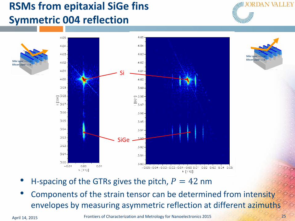
RSMs from epitaxial SiGe fins Symmetric 004 reflection
x1
x2
x3
Si fins SiGe fins
Thin-film Planar
(a) (b)
(c) (d)
x1
x2
x3
Si fins SiGe fins
Thin-film Planar
(a) (b)
(c) (d)
Si
SiGe
• H-spacing of the GTRs gives the pitch, 𝑃 = 42 nm
• Components of the strain tensor can be determined from intensity envelopes by measuring asymmetric reflection at different azimuths

26 Frontiers of Characterization and Metrology for Nanoelectronics 2015 April 14, 2015
RSMs from epitaxial SiGe fins Asymmetric 113ge reflection
x1
x2
x3
Si fins SiGe fins
Thin-film Planar
(a) (b)
(c) (d)
x1
x2
x3
Si fins SiGe fins
Thin-film Planar
(a) (b)
(c) (d)
Si
SiGe
• SiGe in a uniaxial stress state, cf. biaxial stress state for thin-films • Elastic relaxation perpendicular to the line direction
• Composition and thickness determined from fitting, x = 25%, t = 39.4 nm
27 Frontiers of Characterization and Metrology for Nanoelectronics 2015
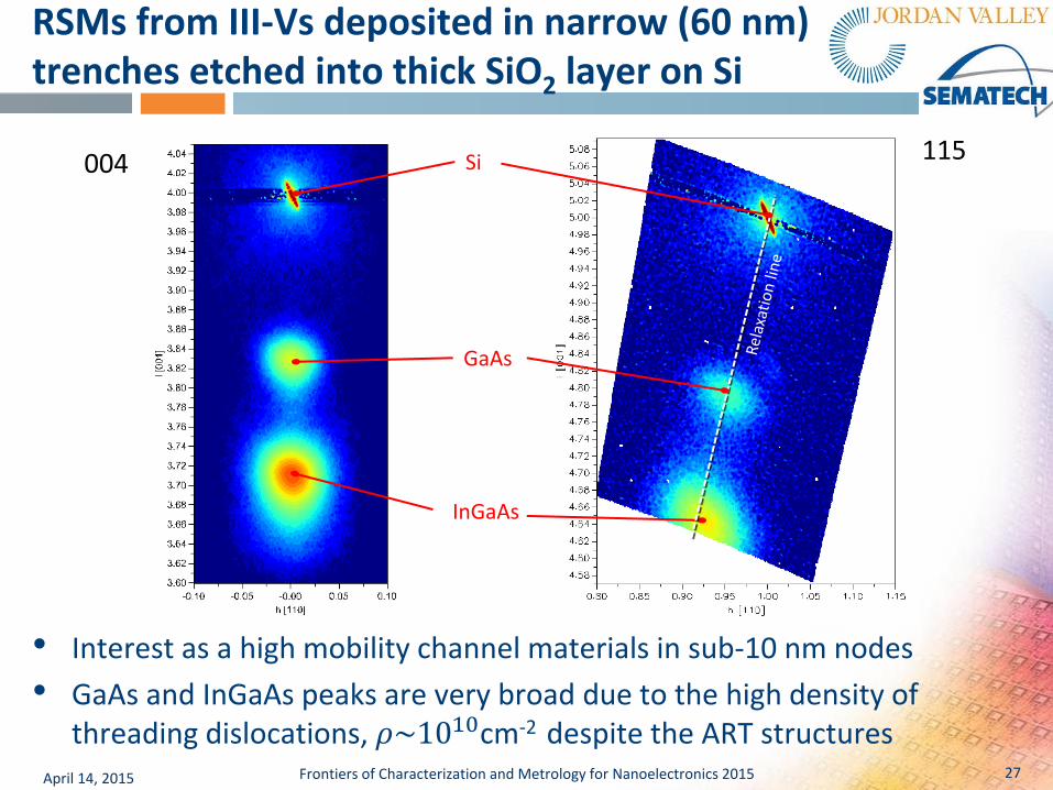
RSMs from III-Vs deposited in narrow (60 nm) trenches etched into thick SiO2 layer on Si
April 14, 2015
• Interest as a high mobility channel materials in sub-10 nm nodes
• GaAs and InGaAs peaks are very broad due to the high density of threading dislocations, 𝜌~1010cm-2 despite the ART structures
004 115 Si
GaAs
InGaAs
28 Frontiers of Characterization and Metrology for Nanoelectronics 2015
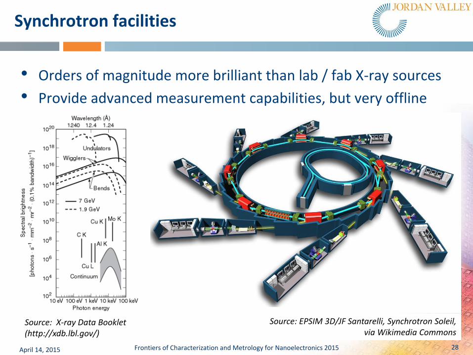
Synchrotron facilities
April 14, 2015
Source: EPSIM 3D/JF Santarelli, Synchrotron Soleil, via Wikimedia Commons
Source: X-ray Data Booklet (http://xdb.lbl.gov/)
• Orders of magnitude more brilliant than lab / fab X-ray sources
• Provide advanced measurement capabilities, but very offline
29 Frontiers of Characterization and Metrology for Nanoelectronics 2015
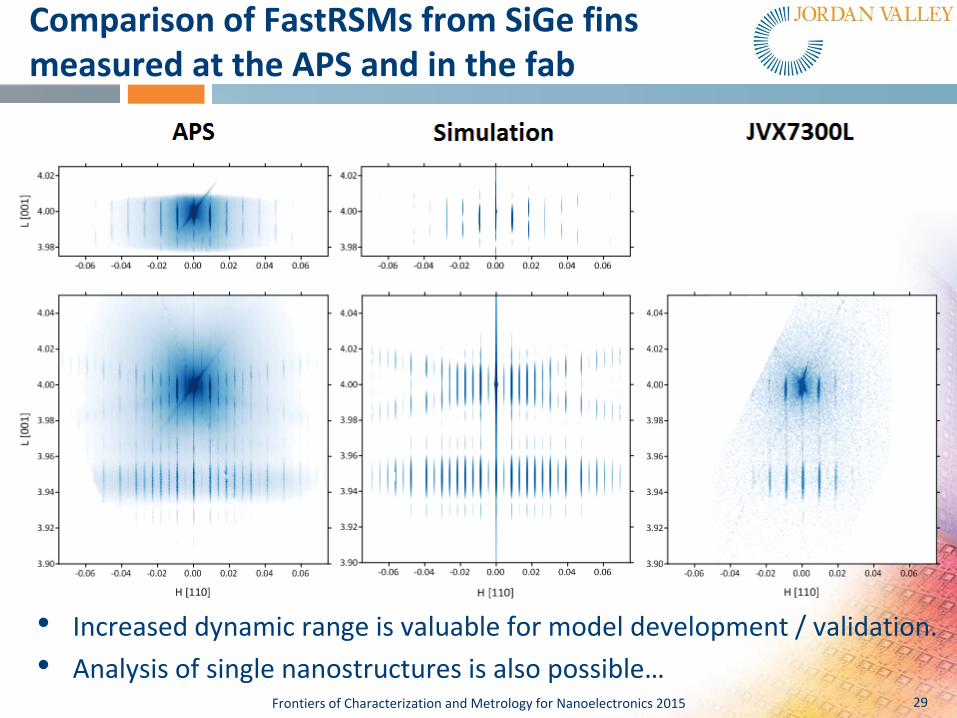
Comparison of FastRSMs from SiGe fins measured at the APS and in the fab
• Increased dynamic range is valuable for model development / validation.
• Analysis of single nanostructures is also possible…

30 Frontiers of Characterization and Metrology for Nanoelectronics 2015
Conclusions
• High-resolution XRD delivers valuable information on epitaxial thin-films and patterned nanostructures • Materials include: SiGe, Si:C(P), Ge and III-Vs for current and future
technology nodes • Parameters include: strain tensor components, composition, thickness,
pitch, pitch-walk, height and SWA as well as crystalline quality
• Complements techniques such as SE / scatterometry and SEM / TEM
• The latest generation of lab / fab tools can yield good quality data in minutes not several hours • From patterned wafers • Including reciprocal space mapping using linear detectors
• In-line X-ray metrology tools, like the JVX7300 series, enable advance materials and process development and provide novel solutions for production monitoring
April 14, 2015

Thank You!
For more information contact us directly or via a
local representative
www.jvsemi.com