high-rate laser micro processing using a polygon scanner...
TRANSCRIPT

HIGH-RATE LASER MICRO PROCESSING USING A POLYGON SCANNER SYSTEM
#M1208
Udo Loeschner
a), Joerg Schille
a), Andre Streek
a), Tommy Knebel
a), Lars Hartwig
a), Robert Hillmann
b),
Christian Endischb)
a) Laserinstitut Hochschule Mittweida, Technikumplatz 17, 09648 Mittweida, Germany
b) SITEC Industrietechnologie GmbH, Bornaer Straße 192, 09114 Chemnitz, Germany
Abstract
This paper discusses results obtained in high-rate laser
micro processing by using a high average power high-
PRF (pulse repetition frequency) ultrashort pulse laser
source in combination with an in-house developed
polygon scanner system.
With the recent development of ultrashort pulse laser
systems supplying high average power of hundreds
watts and megahertz pulse repetition rates, a signifi-
cant increase of the productivity can potentially be
achieved in micro machining. This permits upscaling
of the ablation rates and large-area processing, gaining
increased interest of the ultrashort pulse laser technol-
ogy for a large variety of industrial processes. Howev-
er, effective implementation of high average power
lasers in micro processing requires fast deflection of
the laser beam. For this, high-rate laser processing by
using polygon scanner systems provide a sustainable
technological solution.
In this study, a picosecond laser system with a maxi-
mum average power of 100 W and a repetition rate up
to 20 MHz was used. In raster scanning using the pol-
ygon scanner, the laser beam with a focus spot diame-
ter of 44 µm was deflected with scan speeds of several
hundred meters per second. The two-dimensional
scanning capability of the polygon scanner supplied a
scan field of 325 mm x 325 mm. The investigations
were focused on high-rate large-area laser ablation of
technical grade stainless steel as well as selective thin
film ablation from bulk substrates. By variation of the
processing parameters laser fluence, as well as tem-
poral and spatial pulse-to-pulse distance, their impact
onto the ablation process was evaluated with respect to
the ablation rate, processing rate, surface quality, and
ablation efficiency.
Introduction
High-PRF ultrashort laser sources supplying high av-
erage laser power of more than 100 W have recently
become available, allowing excellent machining quali-
ty and high processing throughput at the same time.
Initial studies in this field are focused on micro vias
generation [1], micro hole processing in steel and cop-
per foils [2], refractive index changes in transparent
materials [3], and laser ablation of micro cavities [4,5].
In addition, the potential of the technology has been
already demonstrated by means of specific machining
examples, such as micro pyramids and embossing tools
[6-9].
The influence of laser fluence and pulse repetition rate
on material removal rate and process efficiency was
studied in [6,9] by using a high-PRF picosecond laser
source. By applying an average laser power of 3 W, a
maximum removal rate of 0.16 mm³/min was achieved
with pulse repetition rates between 50 kHz and
100 kHz. Due to constant average laser power, the
pulse energy was gradually reduced while the pulse
repetition rate increased up to 300 kHz, causing the
decrease of the ablation rates. Furthermore, higher
ablation rates can be achieved performing multi pass
irradiation in the “low-fluence” regime while the laser
fluence is above the threshold limit. Therefore, it has
been shown that the material removal rate can be in-
creased up to 7 mm³/min at a pulse repetition rate of
20 MHz [10].
However, by using high-PRF laser sources fast beam
deflection systems are required prospectively permit-
ting a processing speed of several 100 m/s. A first
approach of a fast laser beam deflection system was
realized by means of an acousto-optic deflector [7].
Therewith a laser engraving process was performed on
the outer mantle of a fast rotating cylinder with a pro-
cessing speed of 40 m/s while the material removal
rate was 3 mm³/min.
Laser micro machining with considerably higher scan
speeds was conducted by the use of a polygon scanner
in combination with a single mode cw fibre laser [11].
In this study processing speeds of 300 m/s have been
demonstrated by irradiating a continuous wave laser
beam of 2 kW laser power and a spot size of 21 µm on
metal sheets.

First results obtained in large-area micro processing
demonstrated once more the potential of the innovative
high-PRF ultrashort pulse laser technology. A ripple
pattern was generated on stainless steel with a dimen-
sion of 80 mm x 80 mm in width and length while the
processing rate was 25 cm²/min [10].
Research activities with high-PRF ultrashort pulse
laser radiation yielded novel phenomena in laser beam
material interaction, those are in contrast to low repeti-
tion rate ultrashort pulse laser processing [2,5,12,13].
On the one hand, a decrease of the ablation rate was
observed with pulse repetition rates of several
100 kHz. For this, plasma shielding induced by inter-
action of the incident laser pulse with the plasma
plume, which originated from the previous laser puls-
es, was suggested. On the other hand, the ablation rate
rises when laser pulses with a frequency in the mega-
hertz range impinge onto the surface of a poor heat-
conducting material like stainless steel, potentially due
heat accumulation effects. Moreover, a further phe-
nomenon called micro cone formation on the scale of
some 10 µm was observed in high-PRF ultrashort
pulse processing with femtosecond laser pulses. Shape,
size, and density of the structures could be influenced
by the laser parameters. Even a selective elimination of
the structures was realized that is in contrast to pico-
second laser pulses [14]. Micro cone formation can
modify the properties of technical grade surfaces with
respect to wettability, roughness, and reflection charac-
teristics.
In conclusion, high average power high-PRF laser
sources combined with ultrafast beam deflection sys-
tems seems to be a promising technology in order to
scale the productivity of high-PRF ultrashort pulse
micromachining with respect to processing throughput
and large-area laser processing. In this work, a novel
machining setup consisting of a high-PRF high average
power picosecond laser source and an ultrafast polygon
scanner was investigated. The study was concentrated
on high-rate ablation of bulk material as well as selec-
tive large-area thin film removal from bulk substrates.
Finally, the potential of this technology was demon-
strated on large-area processed samples.
Experimental
In this study, a high-PRF picosecond laser source of
the PX series from Edgewave GmbH emitting a linear-
ly polarized Gaussian beam at the fundamental wave-
length of 1064 nm was used. Including all losses in the
optical beam path the laser supplied an average power
of 75.9 W onto the work piece surface. The maximum
repetition rate was 20 MHz while the pulse width was
10 ps. Further, the maximum available single pulse
energy decreased with rising repetition rate as a conse-
quence of limited average laser power.
For ultrafast beam deflection across the sample surface
an in-house developed polygon scanner was utilized.
As a special feature the polygon scanner system is
equipped with an additional deflection unit permitting
two-dimensional raster scanning. The laser beam was
focused onto the material surface with a spot size of
44 µm by using an f-theta objective which allows a
maximum scan field of 325 mm x 325 mm. With this
setup scan speeds vsc up to 800 m/s were achieved.
In general, the maximum utilization rate ηf,max of a
single polygon facet was limited by the technical fac-
tors of the geometrical arrangement of the optical
components of the polygon scanner. For the polygon
scanner used in this study, the maximum utilization
rate ηf,max was determined to be 49 %. With respect to
the used f-theta objective, this corresponds to a maxi-
mum processable length lmax of 325 mm. In conclusion,
for laser processing with the maximum possible length
lmax of 325 mm performed with more than one facet a
duty cycle with a ratio of 49:51 has to be considered.
As a result, the maximum achievable effective pro-
cessing speed veff,max corresponds to the duty cycle and
is approximately half of the scan speed vsc, see equa-
tion 1:
Furthermore, a shorter processing length results in a
less effective speed veff given by the ratio ηf of the
current processed length lc and the maximum length
lmax. Hence, the effective processing speed veff can be
calculated with equation 2:
In this study the ablation characteristics of two differ-
ent types of materials were investigated: 1.5 mm thick
technical grade stainless steel (AISI 304) for high-rate
volume ablation and a 75 nm thick silicon nitride thin
film deposited on a multi crystalline silicon wafer in
order to demonstrate high-rate large-area ablation.
To identify the maximum achievable removal rate
cavities were processed into stainless steel by using the
“line-by-line” and “layer-by-layer” raster scan regime
characterized by the lateral pulse distance dp between
two consecutive incident pulses and the hatch distance
dh between lines. Dc is the cavity depth, and ns is the
number of scans representing the quantity of processed
layers. The averaged ablated volume per single pulse
Vsp can be calculated according to equation 3, taken
from [15]:
(1).
(2).
The cavity depth dc was determined at five individual
positions at the cavity bottom by means of a confocal
point sensor µScan from NanoFocus AG. From equa-
tion 3 the ablation rate dz can be estimated considering
the average number of incident laser pulses per area
associated with the focal spot radius w0:
The material removal rate MRR as an indicator for the
process efficiency results from the averaged ablated
volume per single pulse Vsp and the repetition rate fr
and is given by equation 5:
For large-area laser processing the efficiency is charac-
terised by the processing rate Ap which can be calculat-
ed with equation 6:
It is noteworthy, that the processing rates Ap are realis-
tic rates provided by the setup because the effective
processing speed veff was used.
The surface roughness Sa was measured in accordance
with ISO 25178 utilizing a measurement arrangement
consisting of the Confocam C101 (confovis) and the
LV100D–U microscope (Nikon). The measurement
data were analysed with the Mountains Map® soft-
ware.
Results and discussion
In this work high-rate laser ablation of stainless steel
by applying an average laser power of 75.9 W of a
high-PRF picosecond laser source and an ultrafast
polygon scanner was studied. Even at the highest pulse
repetition rate of 20 MHz the supplied laser fluence at
the material surface of 0.5 J/cm² exceeds the ablation
threshold for stainless steel Hth ~ 0.1-0.15 J/cm² by a
factor of 4.
The ablation experiments were carried out by applying
the maximum average laser power of 75.9 W onto the
stainless steel surface while the lateral pulse distance
and the hatch distance between lines were kept con-
stant at 10 µm. By variation of the repetition rate be-
tween 1 MHz and 20 MHz the laser fluence dropped
continually beginning at 10 J/cm² at 1 MHz down to
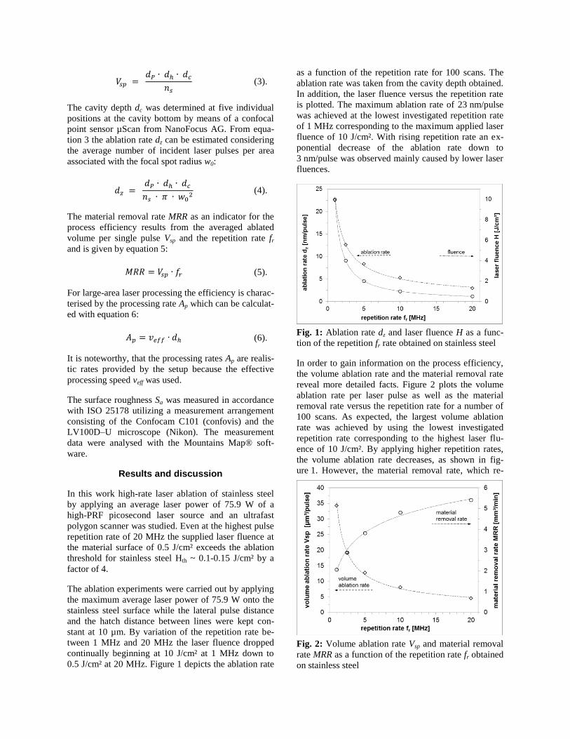
0.5 J/cm² at 20 MHz. Figure 1 depicts the ablation rate
as a function of the repetition rate for 100 scans. The
ablation rate was taken from the cavity depth obtained.
In addition, the laser fluence versus the repetition rate
is plotted. The maximum ablation rate of 23 nm/pulse
was achieved at the lowest investigated repetition rate
of 1 MHz corresponding to the maximum applied laser
fluence of 10 J/cm². With rising repetition rate an ex-
ponential decrease of the ablation rate down to
3 nm/pulse was observed mainly caused by lower laser
fluences.
In order to gain information on the process efficiency,
the volume ablation rate and the material removal rate
reveal more detailed facts. Figure 2 plots the volume
ablation rate per laser pulse as well as the material
removal rate versus the repetition rate for a number of
100 scans. As expected, the largest volume ablation
rate was achieved by using the lowest investigated
repetition rate corresponding to the highest laser flu-
ence of 10 J/cm². By applying higher repetition rates,
the volume ablation rate decreases, as shown in fig-
ure 1. However, the material removal rate, which re-
(3).
(4).
(5).
(6).
Fig. 1: Ablation rate dz and laser fluence H as a func-
tion of the repetition fr rate obtained on stainless steel
Fig. 2: Volume ablation rate Vsp and material removal
rate MRR as a function of the repetition rate fr obtained
on stainless steel

sults from scaling of the volume ablation rate with the
repetition rate increased with rising repetition rate
although the amount of the volume ablation rate
dropped. The maximum material removal rate was
found to be 5.4 mm³/min at a laser fluence of 0.5 J/cm²
and a repetition rate of 20 MHz. The highest ablation
efficiency for ultrashort laser pulses was indicated for
laser fluences about 7.4 times above the ablation
threshold [16]. Within the presented investigations
performed with a picosecond laser system, the supplied
fluence at the highest material removal rate exceeds
the threshold fluence by a factor of 4. So it can be
assumed, that the material removal rate can be maxim-
ized by irradiating laser pulses with a laser fluence in
the range of 0.8 J/cm². For this, a higher average laser
power is needed. It is noteworthy to point out, that the
maximum material removal rate of 5.4 mm³/min is
related to the scan speed of the polygon scanner, which
was 200 m/s. Considering the maximum utilization
rate of the polygon scanner of 49 % used in the inves-
tigations the maximum effective speed was 98 m/s
yielding to a maximum material removal rate of
2.65 mm³/min.
In ultrashort pulse laser processing there is a contro-
versial discussion regarding efficiency analyses be-
tween picosecond laser ablation and femtosecond laser
ablation. The maximum achieved material removal rate
of 5.4 mm³/min in stainless steel, based on the scan
speed, is lower in comparison to the removal rate per-
formed with high-PRF femtosecond laser pulses re-
ported in [10]. There, a scan speed based material
removal rate of 6.8 mm³/min was determined with an
applied laser fluence of 0.85 J/cm² and a repetition rate
of 19.3 MHz by using a galvanometer scanner system.
While the material removal rate achieved with femto-
second laser pulses was obtained at the optimum laser
fluence of 8 times above the threshold level, the rate
for picosecond laser pulses was lower whereas the
applied fluence was below the optimum fluence.
Against this background, similar material removal
rates can be assumed at identical laser fluences. There-
fore, at first glance there is no preference in efficiency
between the picosecond and the femtosecond regime.
But, if the average laser power input is taken into ac-
count, in the picosecond regime an average laser power
of 75.9 W was applied. The investigations with femto-
second laser pulses were performed with an average
laser power of only 31.7 W. To put the rates on a com-
parable basis, the rates were normalized with the laser
power leading to a material removal rate of
0.09 mm³/W/min and 0.21 mm³/W/min for picosecond
laser pulses and femtosecond laser pulses, respectively.
Even though identical material removal rates of
6.8 mm³/min, the laser-power-normalized rates differ
by a factor of more than two indicating a more effi-
cient ablation process of stainless steel for processing
with femtosecond laser pulses.
For a constant total energy input within the ablation
process two different regimes were compared: the
“high-fluence” regime with 10 J/cm² and the “low-
fluence” regime with 0.5 J/cm². Because of the maxi-
mum average laser power of 75.9 W the repetition rate
was 1 MHz for 10 J/cm². Choosing the maximum
repetition rate of 20 MHz the laser fluence of the puls-
es irradiated to the material surface amounts to be
0.5 J/cm². In order to provide a constant total energy
input in the “high-fluence” regime 100 scans and in the
“low-fluence” regime 2000 scans were performed.
Furthermore, the processing time was identically. For
the “high-fluence” regime a volume ablation rate of
2.05 mm³/min was achieved. However, in the “low-
fluence” regime an increase of the ablation rate of
2.58 mm³/min was obtained corresponding to a growth
of 25%.
Beside the ablation rates the surface quality and the
roughness of the ablated areas was evaluated. In fig-
ure 3 SEM photographs are presented, demonstrating
the surface morphology obtained with various laser
fluences.It can be seen, that the surface quality was
strongly influenced by the applied processing parame-
ters. The smoothest surface was obtained by applying
the lowest fluence of 0.5 J/cm² and the highest repeti-
tion rate of 20 MHz. Highly regular ripple formation
with a spatial period of around one micron, which
correlates with the laser wavelength of 1064 nm of the
laser beam [17-21], as well as starting micro crater
development in the grooves between ripples can be
seen. Neither debris nor molten bulges can be observed
on the structure surface indicating a minor thermal
load of the material in spite of high average power
impinging on the sample. This is the result of the low
applied laser fluence of 0.5 J/cm² and very high scan
speed of 200 m/s. Further, with increasing laser flu-
ence the surface appears more roughly. On the bottom
of the cavity micro craters became more pronounced,
growing into deeper regions followed by formation of
micro cones when laser fluence was increased up to the
“high-fluence” regime with gradually lower scan speed
down to 10 m/s at a laser fluence of 10 J/cm². The
surface structures were covered with ripples.
The results of surface roughness measurement, listed
in figure 3f), correlate with the surface morphologies
presented in figure 3a)-e). The smoothest surface,
achieved with the highest repetition rate of 20 MHz
and the lowest laser fluence of 0.5 J/cm² is character-
ised by a surface roughness of 0.6 µm. Surface rough-
ness increases with higher laser fluences and sinking

repetition rates due to pronounced formation of micro
craters and micro cones. The achieved roughness value
of 1.9 µm at a laser fluence of 2 J/cm² is close to the
value reported in [22]. In similar experiments in stain-
less steel, performed with picosecond laser radiation at
a fluence of 2 J/cm², a repetition rate of 150 kHz, and a
comparable ratio between lateral pulse distance and
focal spot diameter, a profile roughness value Ra of
1.6 µm was determined. In conclusion, by applying
low fluences and high repetition rates, maximum mate-
rial removal rates and best surface quality was
achieved at the same time. These results show a similar
tendency observed and discussed in high-PRF laser
ablation with femtosecond laser pulses [10].
figure 3a) 3b) 3c) 3d) 3e)
dp, dc [µm] 10
H [J/cm²] 10 4 2 1 0.5
fr [MHz] 1 2.5 5 10 20
Sa [µm] 3.3 3.1 1.9 1.1 0.6
Fig. 3: a) - e) SEM photographs demonstrate the surface morphology at the cavity bottom obtained with different
processing parameter sets, f) parameters and corresponding roughness values
f)

Up to now, laser micro processing was limited on
comparatively small areas of a few square centimetres.
However, with the investigated laser system a maxi-
mum scan field of 325 mm x 325 mm corresponding to
an area of 0.1 m² can be processed in one pass. The
surface of a stainless steel sheet with a dimension of
265 mm in length and 250 mm in width was laser
processed, presented in figure 4.
With laser pulses supplied at a repetition rate of
20 MHz and a lateral pulse distance of 40 µm, a scan
speed of 800 m/s was realized. If the current processed
length of 265 mm is taken into account, an effective
processing speed of 320 m/s resulted. Further, it yield-
ed to a processing rate of 7680 cm²/min for one scan
which is evident with a processing time of 5.2 s while
the hatch distance was also 40 µm. On closer inspec-
tion, the processed field is characterized by barrel and
pincushion distortion arising from the so far uncorrect-
ed optical system of the polygon scanner. However,
the scanner control provides a feature for scan field
correction which will be tackled in a next step in order
to improve the accuracy of the scanner system.
High-rate large-area laser ablation of a thin film was
conducted on 6” (156 mm x 156 mm) multi crystalline
silicon wafers covered with an approximately 75 nm
thick silicon nitride layer for photovoltaic application.
The challenge of the investigation was to remove the
layer within one pass without any damage of the sili-
con substrate.
First, a grid of lines with a hatch distance of 100 µm
was laser processed by applying a fluence of 1 J/cm²
and a repetition rate of 10 MHz while the lateral pulse
distance was 20 µm corresponding to a scan speed of
200 m/s. Figure 5 shows an optical microscope image
of the processed wafer.
Fig. 5: Selective ablated lines of a silicon nitride layer
on a silicon wafer (line distance: 100 µm, width of
ablated lines: 30 µm)
The silicon nitride layer was completely removed
within the lines showing a width of 30 µm without
damage of the underlying silicon. Considering the
effective processing speed a processing rate of
2800 cm²/min was obtained yielding to a processing
time of the entire wafer surface of 5.2 s. A more de-
tailed consideration revealed slight variations of the
hatch distance between adjacent lines. This is due to
insufficient manufacturing precision of the polygon
wheel, which is also a task of prospective scan field
correction. By applying a laser fluence of 2 J/cm², a
repetition rate of 5 MHz, a lateral pulse distance and a
hatch distance of 20 µm, and a resulting scan speed of
100 m/s the silicon nitride layer was completely re-
moved from the silicon wafer. For a processed field of
136 mm x 136 mm the processing rate was 245 cm²/s
Fig. 4: Laser processed stainless steel surface, field
size 265 mm x 250 mm
Fig. 6: Selective thin film ablation of a silicon nitride
layer using a special feature of the polygon scanner –
multiple segments regime within one facet passing the
laser beam at a scan speed of 200 m/s, line segment
width 4 mm

according to a processing time of 45.5 s. As a special
feature of the polygon scanner multiple line segments
can be produced while one facet passes the laser beam
realized with fast laser switching as a preliminary stage
of a so called pixel mode. The challenge is an exact
timing of the scanner and the control at high scan
speed in order to process the adjacent line segments
with a high lateral precision. The performance capabil-
ity was demonstrated by selective ablation of the sili-
con nitride layer, shown in figure 6. The pattern con-
sisted of 16 ablated fields with a line segment width of
4 mm processed at a scan speed of 200 m/s. It is re-
markable, that there is only a marginal spatial jitter
regarding the starting points of the line segments, at-
testing a very high degree of temporal synchronization
of the scanner system.
Summary
High-rate laser micro processing by using a high aver-
age power high-PRF picosecond laser source in com-
bination with an in-house developed polygon scanner
system, equipped with a two-dimensional scanning
capability, has been investigated in this study. By ap-
plying a raster scanning regime, high-rate ablation of
bulk material as well as high-rate large-area processing
was analysed in detail.
Stainless steel was irradiated with a maximum average
laser power of 75.9 W. The highest material removal
rate of 5.4 mm³/min was achieved in the “low-fluence”
regime at the highest available repetition rate of
20 MHz. In addition, with these parameters the best
surface quality was obtained, characterized by a mini-
mum surface roughness of 0.6 µm.
With the presented laser system the capability of high-
rate large-area laser processing was demonstrated on a
stainless steel sheet. A field size of 265 mm in length
and 250 mm in width was processed with a processing
rate of 7680 cm²/min for one scan. Further, thin film
ablation of a silicon nitride layer from bulk silicon
substrate was investigated. The layer was completely
removed in one pass in a field of 136 mm x 136 mm
without any damage of the silicon while the processing
rate was 245 cm²/min. Furthermore, selective thin film
removal was performed. For this, a grid of lines with a
hatch distance of 100 µm was laser processed with a
processing rate of 2800 cm²/min.
Acknowledgment
The presented results have been conducted in the
course of the projects ”Innoprofile Transfer – Rapid
Micro/Hochrate-Laserbearbeitung” (03IPT506X),
funded by the Federal Ministry of Education and Re-
search.
References
[1] Tan, B., Panchatsharam, S., Venkatakrishnan, K.
(2009) High repetition rate femtosecond laser forming
sub-10μm diameter-interconnection vias, J. Phys. D:
Appl. Phys. 42.
[2] Ancona, A., Röser, F., Rademaker, K., Limpert,
J., Nolte, S., Tünnermann, A. (2008) High speed laser
drilling of metals using a high repetition rate, high
average power ultrafast fiber CPA system, Optics
Express Vol. 16, No. 12.
[3] Yoshino, F., Shah, L., Fermann, M., Arai, A.,
Uehara, Y. (2008) Micromachining with a high repeti-
tion rate femtosecond laser, J. Laser Micro Nanoeng.
3(3), 157–162.
[4] Lopez, J., Loumena, C., Zaouter, Y., Mottay, E.
(2010) Micromachining of metal and silicon using high
average power ultrafast fiber laser, in Proceedings of
LPM2010-the 11th International Symposium on Laser
Precision Microfabrication, Stuttgart (GER).
[5] Schille, J., Ebert, R., Löschner, U., Regenfuß, P.,
Süß, T., Exner, H. (2008) Micro structuring with high-
ly repetitive ultra short laser pulses, in Proceedings of
LPM2008-the 9th International Symposium on Laser
Precision Microfabrication, 16.-20.6.2008, Quebec,
Canada.
[6] Neuenschwander, B., Bucher, G.F., Nussbaum,
C., Joss, B., Muralt, M., Hunziker, U.W., Schuetz, P.
(2010) Processing of metals and dielectric materials
with ps-laserpulses: results, strategies, limitations and
needs in Proceedings of SPIE 7584, Laser Applications
in Microelectronic and Optoelectronic Manufacturing
XV, 75840R); doi:10.1117/12.846521.
[7] Bruening, S., Hennig, G., Eifel, S., Gillner, A.
(2011) Ultrafast scan techniques for 3D-μm structuring
of metal surfaces with high repetitive ps-laser pulses,
Physics Procedia, 12, Part B(0): p. 105-115.
[8] Knappe, R., Brüning, S., Gillner, A. (2011)
Kleinste Strukturen auf großen Flächen, Laser Technik
Journal, 8(4): p. 24-27.
[9] Neuenschwander, B., Bucher, G.F., Hennig, G.,
Nussbaum, C., Joss, B., Muralt, M., Zehnder, S.,
Hunziker, U.W., Schuetz, P. (2010) Processing of
dielectric materials and metals with ps laserpulses, in
Proceedings of 29th Intern. Congress on Applications
of Lasers & Electro-Optics (ICALEO), paper M101,
Anaheim, California, USA.

[10] Schille, J., Schneider, L., Mueller, M., Loeschner,
U., Goddard, N., Scully, P., Exner, H. (2013) High-
speed Laser Micro Processing using Ultrashort Laser
Pulses, in Proceedings of LAMP2013 - the 6th Interna-
tional Congress on Laser Advanced Materials Pro-
cessing.
[11] Exner, H., Hartwig, L., Ebert, R., Kloetzer, S.,
Streek, A., Schille, J., Loeschner, U. (2010) High rate
laser micro processing using high brilliant cw laser
radiation, in Proceedings of the 11th International
Symposium on Laser Precision Microfabrication
(LPM) 2010, 07.-10.06.2010, Stuttgart, Germany.
[12] Döring, S., Ancona, A., Hädrich, S., Limpert, J.,
Nolte, S., Tünnermann, A. (2010) Microdrilling of
metals using femtosecond laser pulses and high aver-
age powers at 515 nm and 1030 nm, Applied Physics
A: Materials Science & Processing, 2010, 100(1): p.
53-56.
[13] Nolte, S., Döring, S., Ancona, A., Limpert, J.,
Tünnermann, A. (2011) High repetition rate ultrashort
pulse micromachining with fiber lasers, Fiber Laser
Applications, 2011, Optical Society of America.
[14] Schille, J., Ebert, R., Loeschner, U., Schneider,
L., Walther, N., Regenfuss, P., Scully, P., Goddard,
N., Exner, H (2009) An ultrafast femtosecond fibre
laser as a new tool in Rapid Microtooling, in Pro-
ceedings of LAMP2009 - the 5th International Con-
gress on Laser Advanced Materials Processing, Kobe
(JAP).
[15] Schille, J., Schneider, L., Loeschner, U., Ebert,
R., Scully, P., Goddard, N., Steiger, B., Exner, H.
(2011) Micro processing of metals using a high repeti-
tion rate femtosecond laser: from laser process parame-
ter study to machining examples, in Proceedings of
ICALEO - 30th International Congress on Applica-
tions of Lasers & Electro-Optics, Orlando, FL (USA).
[16] Raciukaitis, G., et al. (2008) Use of High Repeti-
tion Rate and High Power Lasers in Microfabrication:
How to Keep the Efficiency High?, LPM2008 - 9th
Symp. on Laser Precision Micromachining, Quebec
(Canada).
[17] Rubahn, H.G., Balzer, F. (2005) Laseranwen-
dungen an harten und weichen Oberflächen (written in
German). Vieweg & Teubner p.308.
[18] Zhou, M., et al. (2009) Sub-wavelength Ripple
Formation on Silicon Induced by Femtosecond Laser
Radiation, Chinese Physics Letters. 26(3): p. 037901.
[19] Gottmann, J., Wortmann, D., Hoerstmann-
Jungemann, M. (2009) Fabrication of sub-wavelength
sur-face ripples and in-volume nanostructures by fs-
laser induced selective etching, Applied Surface Sci-
ence, 2009. 255(10): p. 5641-5646.
[20] Wang, X., et al. (2005) Femtosecond pulsed la-
ser-induced periodic surface structures on
GaN/sapphire, Applied Surface Science, 2005. 252(5):
p. 1492-1497.
[21] Hou, S., et al. (2011) Formation of long-and
short-periodic nanoripples on stainless steel irradiated
by femtosecond laser pulses, Journal of Physics D:
Applied Physics 44(50): p. 505401.
[22] Lickschat. P., Schille, J., Mueller, M., Weißman-
tel, S., Reiße, G. (2012) Comparative study on micro-
structuring of steel using pico- and femtosecond laser
pulses, in Proceedings of ICALEO - 31st Interna-tional
Congress on Applications of Lasers & Electro-Optics,
Anaheim, Ca. (USA), 1261-1268.
Meet the author
Udo Loeschner is graduated in Physical Engineering
from the University of Applied Sciences Mittweida
(Germany) in 1998. Thereafter he has been a R&D
engineer at the laser institute of the same university.
Since 2006 he joined the Rapid Micro Tooling re-
search group to investigate laser micro processing with
short and ultrashort pulse laser technologies. He com-
pleted his PhD thesis at the Technische Universitaet
Ilmenau in 2007. In 2011 he became an endowed pro-
fessorship and represents the appointment area “High
rate laser processing”.