high-performance sab 80c517a/83c517a-5 8-bit cmos single...
TRANSCRIPT

05.94
High-Performance SAB 80C517A/83C517A-58-Bit CMOS Single-Chip Microcontroller
Preliminary
SAB 83C517A-5 Microcontroller with factory mask-programmable ROMSAB 80C517A Microcontroller for external ROM
SAB 80C517A/83C517A-5, Eight data pointers for external memoryup to 18 MHz operation addressing
32 K × 8 ROM (SAB 83C517A-5 only, Seventeen interrupt vectors, four priorityROM-Protection available) levels selectable
256 × 8 on-chip RAM Genuine 10-bit A/D converter with 2 K × 8 on-chip RAM (XRAM) 12 multiplexed inputs Superset of SAB 80C51 architecture: Two full duplex serial interfaces with
– 1 µs instruction cycle time at 12 MHz programmable Baudrate-Generators– 666 ns instruction cycle time at 18 MHz Fully upward compatible with SAB 80C515,– 256 directly addressable bits SAB 80C517, SAB 80C515A– Boolean processor Extended power saving mode– 64 Kbyte external data and Fast Power-On Reset
program memory addressing Nine ports: 56 I/O lines, 12 input lines Four 16-bit timer/counters Three temperature ranges available: Powerful 16-bit compare/capture unit 0 to 70 oC (T1)
(CCU) with up to 21 high-speed or PWM – 40 to 85oC (T3)output channels and 5 capture inputs – 40 to 110oC (T4)
Versatile "fail-safe" provisions Plastic packages: P-LCC-84, Fast 32-bit division, 16-bit multiplication, P-MQFP-100-2
32-bit normalize and shift by peripheral MUL/DIV unit (MDU)
The SAB 80C517A/83C517A-5 is a high-end member of the Siemens SAB 8051 family ofmicrocontrollers. It is designed in Siemens ACMOS technology and based on SAB 8051architecture. ACMOS is a technology which combines high-speed and density characteristicswith low-power consumption or dissipation.
While maintaining all the SAB 80C517 features and operating characteristics theSAB 80C517A is expanded in its "fail-safe" characteristics and timer capabilities.TheSAB 80C517A is identical with the SAB 83C517A-5 except that it lacks the on-chip programmemory. The SAB 80C517A/83C517A-5 is supplied in a 84-pin plastic leaded chip carrierpackage (P-LCC-84) and in a 100-pin plastic quad flat package (P-MQFP-100-2).

SAB 80C517A/83C517A-5
Semiconductor Group 2
SAB 80C517A/83C517A-5Revision History 05.94
Previous Releases 01.94/08.93/11.92/10.91/04.91
Page Subjects (changes since last revision 04.91)
546-14several 225,26,30
333957606265
several6668
– Pin configuration P-MQFP-100-2 added– Pin differences updated– Pin numbers for P-MQFP-100-2 package added– Correction of P-MRFP-100 into P-MQFP-100-2– Ordering information for -40 to +110°C versions– Correction of register names S0RELL, SCON, ADCON, ICRON, and SBUF– Figure 4 corrected– Figure 8 corrected– PE/SWD function description completed– Correct ordering numbers– Test condition for VOH, VOH1 corrected– tPXIZ name corrected
tAVIV, tAZPL values corrected– Minimum clock frequence is now 3.5 MHz– tQVWH (data setup before WR) corrected and added– tLLAX2 corrected
Page Subjects (changes since last revision 08.93)
2551
656774
– Corrected SFR name S0RELL– Below "Termination of HWPD Mode": 4th paragraph with ident corrected– Description of tLLIV corrected– Program Memory Read Cycle: tPXAV added– Oscillator circuit drawings: MQFP-100-2 pin numbers added.
Page Subjects (changes since last revision 01.94)
47– Minor changes on several pages– Table 6 corrected

SAB 80C517A/83C517A-5
Semiconductor Group 3
Ordering Information
Type Orderingcode
Package Description8-bit CMOS microcontroller
SAB 80C517A-N18 Q67120-C583 P-LCC-84for external memory,18 MHz
SAB 80C517A-M18 TBD P-MRFP-100
SAB 83C517A-5N18 Q67120-C582 P-LCC-84 with mask-programmable ROM,18 MHz
SAB 80C517A-N18-T3 Q67120-C769 P-LCC-84 for external memory,18 MHzext. temperature – 40 to 85 oC
SAB 83C517A-5N18-T3 Q67120-C771 P-LCC-84 with mask-programmable ROM,18 MHzext. temperature – 40 to 85 oC
SAB 83C517A-N18-T4 TBD P-LCC-84 for external memory, 18 MHzext. temperature -40 to +110oC
SAB 83C517A-5N18-T4 TBD P-LCC-84 with mask-programmable ROM,18 MHzext. temperature -40 to +110oC

SAB 80C517A/83C517A-5
Semiconductor Group 4
Logic Symbol

SAB 80C517A/83C517A-5
Semiconductor Group 5
The pin functions of the SAB 80C517A are identical with those of the SAB 80C517/80C537 withone exception:
Typ SAB 80C517A SAB 80C517/80C537
P-LCC-84, Pin 60HWPD N.C.
P-MQFP-100-2,Pin 36
Pin Configuration(P-LCC-84)

SAB 80C517A/83C517A-5
Semiconductor Group 6
Pin Configuration(P-MQFP-100-2)

SAB 80C517A/83C517A-5
Semiconductor Group 7
Pin Definitions and Functions
Symbol Pin Number I/O *) Function
P-LCC-84 P-MQFP-100-2
P4.0 – P4.7 1– 3, 5 – 9 64 - 66,68 - 72
I/O Port 4is a bidirectional I/O port with internalpull-up resistors. Port 4 pins that have 1s written to them are pulled high by theinternal pull-up resistors, and in thatstate can be used as inputs. As inputs,port 4 pins being externally pulled lowwill source current (IIL, in the DC char-acteristics) because of the internal pull-up resistors.This port also serves alternate comparefunctions. The secondary functions areassigned to the pins of port 4 as follows:– CM0 (P4.0): Compare Channel 0– CM1 (P4.1): Compare Channel 1– CM2 (P4.2): Compare Channel 2– CM3 (P4.3): Compare Channel 3– CM4 (P4.4): Compare Channel 4– CM5 (P4.5): Compare Channel 5– CM6 (P4.6): Compare Channel 6– CM7 (P4.7): Compare Channel 7
PE/SWD 4 67 I Power saving modes enable StartWatchdog TimerA low level on this pin allows the soft-ware to enter the power down, idle andslow down mode. In case the low levelis also seen during reset, the watchdogtimer function is off on default.Use of the software controlled powersaving modes is blocked, when this pinis held on high level. A high level duringreset performs an automatic start of thewatchdog timer immediately after reset.When left unconnected this pin is pulledhigh by a weak internal pull-up resistor.
* I = InputO = Output

SAB 80C517A/83C517A-5
Semiconductor Group 8
Pin Definitions and Functions (cont’d)
Symbol Pin Number I/O *) Function
P-LCC-84 P-MQFP-100-2
RESET 10 73 I RESETA low level on this pin for the duration ofone machine cycle while the oscillator isrunning resets the SAB 80C517A. Asmall internal pull-up resistor permitspower-on reset using only a capacitorconnected to VSS.
V AREF 11 78 Reference voltage for the A/D con-verter.
V AGND 12 79 Reference ground for the A/Dconverter.
P7.7 -P7.0 13 - 20 80 - 87 I Port 7is an 8-bit unidirectional input port. Portpins can be used for digital input, ifvoltage levels meet the specified inputhigh/low voltages, and for the lower 8-bit of the multiplexed analog inputs ofthe A/D converter, simultaneously.
* I = InputO = Output

SAB 80C517A/83C517A-5
Semiconductor Group 9
Pin Definitions and Functions (cont’d)
Symbol Pin Number I/O *) Function
P-LCC-84 P-MQFP-100-2
P3.0 - P3.7 21 - 28 90 - 97 I/O Port 3is a bidirectional I/O port with internal pull-up resistors. Port 3 pins that have 1 swritten to them are pulled high by theinternal pull-up resistors, and in that statecan be used as inputs. As inputs, port 3pins being externally pulled low will sourcecurrent (IIL, in the DC characteristics)because of the internal pull-up resistors.Port 3 also contains the interrupt, timer,serial port 0 and external memory strobepins that are used by various options. Theoutput latch corresponding to a secondaryfunction must be programmed to a one (1)for that function to operate.
The secondary functions are assigned tothe pins of port 3, as follows:
– R × D0 (P3.0): receiver data input(asynchronous) or data input/output(synchronous) of serial interface
– T × D0 (P3.1): transmitter data output(asynchronous) or clock output(synchronous) of serial interface 0
– INT0 (P3.2): interrupt 0 input/timer 0gate control
– INT1 (P3.3): interrupt 1 input/timer 1gate control
– T0 (P3.4): counter 0 input
– T1 (P3.5): counter 1 input
– WR (P3.6): the write control signallatches the data byte from port 0 into theexternal data memory
– RD (P3.7): the read control signalenables the external data memory toport 0
* I = InputO = Output
SAB 80C517A/83C517A-5
Semiconductor Group 10
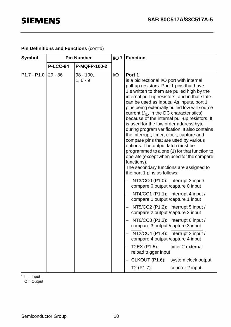
P1.7 - P1.0 29 - 36 98 - 100,1, 6 - 9
I/O Port 1is a bidirectional I/O port with internalpull-up resistors. Port 1 pins that have1 s written to them are pulled high by theinternal pull-up resistors, and in that statecan be used as inputs. As inputs, port 1pins being externally pulled low will sourcecurrent (IIL, in the DC characteristics)because of the internal pull-up resistors. Itis used for the low order address byteduring program verification. It also containsthe interrupt, timer, clock, capture andcompare pins that are used by variousoptions. The output latch must beprogrammed to a one (1) for that function tooperate (except when used for the comparefunctions).The secondary functions are assigned tothe port 1 pins as follows:
– INT3/CC0 (P1.0): interrupt 3 input/compare 0 output /capture 0 input
– INT4/CC1 (P1.1): interrupt 4 input /compare 1 output /capture 1 input
– INT5/CC2 (P1.2): interrupt 5 input /compare 2 output /capture 2 input
– INT6/CC3 (P1.3): interrupt 6 input /compare 3 output /capture 3 input
– INT2/CC4 (P1.4): interrupt 2 input /compare 4 output /capture 4 input
– T2EX (P1.5): timer 2 externalreload trigger input
– CLKOUT (P1.6): system clock output
– T2 (P1.7): counter 2 input
* I = InputO = Output
Pin Definitions and Functions (cont’d)
Symbol Pin Number I/O *) Function
P-LCC-84 P-MQFP-100-2

SAB 80C517A/83C517A-5
Semiconductor Group 11
XTAL2 39 12 – XTAL2Input to the inverting oscillator amplifier andinput to the internal clock generator circuits.
XTAL1 40 13 – XTAL1Output of the inverting oscillator amplifier.To drive the device from an external clocksource, XTAL2 should be driven, whileXTAL1 is left unconnected. There are norequirements on the duty cycle of theexternal clock signal, since the input to theinternal clocking circuitry is devided downby a divide-by-two flip-flop. Minimum andmaximum high and low times as well asrise/fall times specified in the ACcharacteristics must be observed.
P2.0 - P2.7 41 - 48 14 - 21 I/O Port 2is a bidirectional I/O port with internal pull-up resistors. Port 2 pins that have 1 swritten to them are pulled high by theinternal pull-up resistors, and in that statecan be used as in-puts. As inputs, port 2pins being externally pulled low will sourcecurrent (IIL, in the DC characteristics)because of the internal pull-up resistors.Port 2 emits the high-order address byteduring fetches from external programmemory and during accesses to externaldata memory that use 16-bit addresses(MOVX @DPTR). In this application it usesstrong internal pull-up resistors whenissuing1 s. During accesses to externaldata memory that use 8-bit addresses(MOVX @Ri), port 2 issues the contents ofthe P2 special function register.
* I = InputO = Output
Pin Definitions and Functions (cont’d)
Symbol Pin Number I/O *) Function
P-LCC-84 P-MQFP-100-2

SAB 80C517A/83C517A-5
Semiconductor Group 12
PSEN 49 22 O The Program Store Enableoutput is a control signal that enables theexternal program memory to the bus duringexternal fetch operations. It is activatedevery six oscillator periodes except duringexternal data memory accesses. Remainshigh during internal program execution.
ALE 50 23 O The Address Latch Enableoutput is used for latching the address intoexternal memory during normal operation.It is activated every six oscillator periodesexcept during an external data memoryaccess
EA 51 24 I External Access EnableWhen held at high level, instructions arefetched from the internal ROM (SAB83C517A-5 only) when the PC is less than8000H. When held at low level, the SAB80C517A fetches all instructions from ex-ternal program memory. For the SAB80C517A this pin must be tied low
P0.0 - P0.7 52 - 59 26 - 27,30 - 35
I/O Port 0is an 8-bit open-drain bidirectional I/O port.Port 0 pins that have 1 s written to themfloat, and in that state can be used as high-impe-dance inputs. Port 0 is also themultiplexed low-order address and databus during accesses to external program ordata memory. In this application it usesstrong internal pull-up resistors whenissuing 1 s. Port 0 also out-puts the codebytes during program verification in theSAB 83C517A if ROM-Protection was notenabled. External pull-up resistors arerequired during program verification.
* I = InputO = Output
Pin Definitions and Functions (cont’d)
Symbol Pin Number I/O *) Function
P-LCC-84 P-MQFP-100-2

SAB 80C517A/83C517A-5
Semiconductor Group 13
HWPD 60 36 I Hardware Power DownA low level on this pin for the duration ofone machine cycle while the oscillator isrunning resets the SAB 80C517A. A lowlevel for a longer period will force the part toPower Down Mode with the pins floating.(see table 7)
P5.7 - P5.0 61 - 68 37 - 44 I/O
I
Port 5is a bidirectional I/O port with internal pull-up resistors. Port 5 pins that have 1 swritten to them are pulled high by theinternal pull-up resistors, and in that statecan be used as inputs. As inputs, port 5pins being externally pulled low will sourcecurrent (IIL, in the DC characteristics)because of the internal pull-up resistors.This port also serves the alternate function"Concurrent Compare" and "Set/ResetCompare". The secondary functions areassigned to the port 5 pins as follows:
– CCM0 to CCM7 (P5.0 to P5.7):concurrent compare or Set/Reset
OWE 69 45 I/O Oscillator Watchdog EnableA high level on this pin enables theoscillator watchdog. When leftunconnected this pin is pulled high by aweak internal pull-up resistor. When held atlow level the oscillator watchdog function isoff.
* I = InputO = Output
Pin Definitions and Functions (cont’d)
Symbol Pin Number I/O *) Function
P-LCC-84 P-MQFP-100-2

SAB 80C517A/83C517A-5
Semiconductor Group 14
P6.0 - P6.7 70 - 77 46 - 50,54 - 56
I/O Port 6is a bidirectional I/O port with internal pull-up resistors. Port 6 pins that have 1 swritten to them are pulled high by theinternal pull-up resistors, and in that statecan be used as inputs. As inputs, port 6pins being externally pulled low will sourcecurrent (I IL, in the DC characteristics)because of the internal pull-up resistors.Port 6 also contains the external A/Dconverter control pin and the transmit andreceive pins for serial channel 1. Theoutput latch corresponding to a secondaryfunction must be programmed to a one (1)for that function to operate.The secondary functions are assigned tothe pins of port 6, as follows:
– ADST (P6.0): external A/D converter start pin
– R × D1 (P6.1): receiver data inputof serial interface 1
– T × D1 (P6.2): transmitter data outputof serial interface 1
P8.0 - P8.3 78 - 81 57 - 60 I Port 8is a 4-bit unidirectional input port. Port pinscan be used for digital input, if voltagelevels meet the specified input high/lowvoltages, and for the higher 4-bit of themultiplexed analog inputs of the A/Dconverter, simultaneously
* I = InputO = Output
Pin Definitions and Functions (cont’d)
Symbol Pin Number I/O *) Function
P-LCC-84 P-MQFP-100-2

SAB 80C517A/83C517A-5
Semiconductor Group 15
Pin Definitions and Functions (cont’d)
Symbol Pin Number I/O *) Function
P-LCC-84 P-MQFP-100-2
RO 82 61 O Reset OutputThis pin outputs the internallysynchronized reset request signal. Thissignal may be generated by an externalhardware reset, a watchdog timer resetor an oscillator watch-dog reset. Thereset output is active low.
VS S 37, 83 10, 62 – Circuit ground potential
VCC 38, 84 11, 63 – Supply Terminal for all operatingmodes
N.C. – 2 - 5, 25,28 - 29,51 - 53,74 - 77,88 - 89
– Not connected
* I = InputO = Output

SAB 80C517A/83C517A-5
Semiconductor Group 16
Figure 1Block Diagram

SAB 80C517A/83C517A-5
Semiconductor Group 17
Functional Description
The SAB 80C517A is based on 8051 architecture. It is a fully compatible member of theSiemens SAB 8051/80C51 microcontroller family being an significantly enhancedSAB 80C517. The SAB 80C517A is therefore compatible with code written for theSAB 80C517.
Having an 8-bit CPU with extensive facilities for bit-handling and binary BCD arithmetics theSAB 80C517A is optimized for control applications. With a 18 MHz crystal, 58 % of theinstructions are executed in 666.67 ns.
Being designed to close the performance gap to the 16-bit microcontroller world, theSAB 80C517A’s CPU is supported by a powerful 32-/16-bit arithmetic unit and a more flexibleaddressing of external memory by eight 16-bit datapointers.
Memory Organisation
According to the SAB 8051 architecture, the SAB 80C517A has separate address spaces forprogram and data memory. Figure 2 illustrates the mapping of address spaces.
Figure 2Memory Map

SAB 80C517A/83C517A-5
Semiconductor Group 18
Program Memory ('Code Space')
The SAB 83C517A-5 has 32 Kbyte of on-chip ROM, while the SAB 80C517A has no internalROM. The program memory can externally be expanded up to 64 Kbyte. Pin EA controlswhether program fetches below address 8000H are done from internal or external memory.
As a new feature the SAB 83C517A-5 offers the possibility of protecting the internal ROMagainst unauthorized access. This protection is implemented in the ROM-Mask.Therefore, thedecision ROM-Protection 'yes' or 'no' has to be made when delivering the ROM-Code. Onceenabled, there is no way of disabling the ROM-Protection.
Effect: The access to internal ROM done by an externally fetched MOVC instructionis disabled. Nevertheless, an access from internal ROM to external ROM is possible.
To verify the read protected ROM-Code a special ROM-Verify-Mode is implemented. Thismode also can be used to verify unprotected internal ROM.
ROM -Protection ROM-Verification Mode(see 'AC Characteristics')
Restrictions
no ROM-Verification Mode 1(standard 8051 Verification Mode)ROM-Verification Mode 2
–
yes ROM-Verification Mode 2 – standard 8051Verification Mode isdisabled
– externally applied MOVCaccessing internal ROMis disabled
SAB 80C517A/83C517A-5
Semiconductor Group 19
Data Memory ('Code Space')
The data memory space consists of an internal and an external memory space. TheSAB 80C517A contains another 2 Kbyte on On-Chip RAM above the 256-bytes internal RAMof the base type SAB 80C517. This RAM is called XRAM in this document.
External Data Memory
Up to 64 Kbyte external data memory can be addressed by instructions that use 8-bit or 16-bitindirect addressing. For 8-bit addressing MOVX instructions in combination with registers R0and R1 can be used. A 16-bit external memory addressing is supported by eight 16-bitdatapointers. Registers XPAGE and SYSCON are controlling whether data fetches ataddresses F800H to FFFFH are done from internal XRAM or from external data memory.
Internal Data Memory
The internal data memory is divided into four physically distinct blocks:
– the lower 128 bytes of RAM including four banks containing eight registers each
– the upper 128 byte of RAM
– the 128 byte special function register area.
– a 2 K × 8 area which is accessed like external RAM (MOVX-instructions), implemented onchip at the address range from F800H to FFFFH. Special Function Register SYSCONcontrols whether data is read or written to XRAM or external RAM.
A mapping of the internal data memory is also shown in figure 2. The overlapping addressspaces are accessed by different addressing modes (see User's Manual SAB 80C517). Thestack can be located anywhere in the internal data memory.
Architecture for the XRAM
The contents of the XRAM is not affected by a reset or HW Power Down. After power-up thecontents is undefined, while it remains unchanged during and after a reset or HW Power Downif the power supply is not turned off.
The additional On-Chip RAM is logically located in the "external data memory" range at theupper end of the 64 Kbyte address range (F800H-FFFFH). It is possible to enable and disable(only by reset) the XRAM. If it is disabled the device shows the same behaviour as the partswithout XRAM, i.e. all MOVX accesses use the external bus to physically external datamemory.

SAB 80C517A/83C517A-5
Semiconductor Group 20
Accesses to XRAM
Because the XRAM is used in the same way as external data memory the same instructiontypes must be used for accessing the XRAM.
Note: If a reset occurs during a write operation to XRAM, the effect on XRAM depends on thecycle which the reset is detected at (MOVX is a 2-cycle instruction):
Reset detection at cycle 1: The new value will not be written to XRAM. The old valueis not affected.
Reset detection at cycle 2: The old value in XRAM is overwritten by the new value.
Accesses to XRAM using the DPTR
There are a Read and a Write instruction from and to XRAM which use one of the 16-bit DPTRfor indirect addressing. The instructions are:
MOVX A, @DPTR (Read)
MOVX @DPTR, A (Write)
Normally the use of these instructions would use a physically external memory. However, in theSAB 80C517A the XRAM is accessed if it is enabled and if the DPTR points to the XRAMaddress space (DPTR F800H).
Accesses to XRAM using the Registers R0/R1
The 8051 architecture provides also instructions for accesses to external data memory rangewhich use only an 8-bit address (indirect addressing with registers R0 or R1). The instructionsare:
MOVX A, @Ri (Read)
MOVX @Ri, A (Write)
In application systems, either a real 8-bit bus (with 8-bit address) is used or Port 2 serves aspage register which selects pages of 256-byte. However, the distinction, whether Port 2 isused as general purpose I/O or as "page address" is made by the external system design. Fromthe device’s point of view it cannot be decided whether the Port 2 data is used externally asaddress or as I/O data!
Hence, a special page register is implemented into the SAB 80C517A to provide the possibilityof accessing the XRAM also with the MOVX @Ri instructions, i.e. XPAGE serves the samefunction for the XRAM as Port 2 for external data memory.

SAB 80C517A/83C517A-5
Semiconductor Group 21
Special Function Register XPAGE
The reset value of XPAGE is 00H.XPAGE can be set and read by software.
The register XPAGE provides the upper address byte for accesses to XRAM with MOVX @Riinstructions. If the address formed from XPAGE and Ri is less than the XRAM address range,then an external access is performed. For the SAB 80C517A the contents of XPAGE must begreater or equal than F8H in order to use the XRAM. Of course, the XRAM must be enabled ifit shall be used with MOVX @Ri instructions.
Thus, the register XPAGE is used for addressing of the XRAM; additionally its contents areused for generating the internal XRAM select. If the contents of XPAGE is less than the XRAMaddress range then an external bus access is performed where the upper address byte isprovided by P2 and not by XPAGE!
Therefore, the software has to distinguish two cases, if the MOVX @Ri instructions with pagingshall be used:
a) Access to XRAM: The upper address byte must be written to XPAGEor P2; both writes selects the XRAM address range.
b) Access to external memory: The upper address byte must be written to P2; XPAGEwill be loaded with the same address in order to deselectthe XRAM.
Addr. 91H XPAGE

SAB 80C517A/83C517A-5
Semiconductor Group 22
Control of XRAM in the SAB 80C517A
There are two control bits in register SYSCON which control the use and the bus operationduring accesses to the additional On-Chip RAM (XRAM).
Special Function Register SYSCON
Reset value of SYSCON is xxxx xx01B.
The control bit XMAP0 is a global enable/disable bit for the additional On-Chip RAM (XRAM).If this bit is set, the XRAM is disabled, all MOVX accesses use external memory via the externalbus. In this case the SAB 80C517A does not use the additional On-Chip RAM and is compatiblewith the types without XRAM.
Addr. 0B1H — — — — — — XMAP1 XMAP0 SYSCON
Bit Function
XMAP0 Global enable/disable bit for XRAM memory.XMAP0 = 0: The access to XRAM (= On-Chip XDATA memory) is en-abled.XMAP0 = 1: The access to XRAM is disabled. All MOVX accesses are per-formed by the external bus (reset state).
XMAP1 Control bit for RD/WR signals during accesses to XRAM; this bit has noeffect if XRAM is disabled (XMAP0 = 1) or if addresses exceeding theXRAM address range are used for MOVX accesses.XMAP1 = 0: The signals RD and WR are not activated during accessesto XRAM.XMAP1 = 1: The signals RD and WR are activated during accesses toXRAM.

SAB 80C517A/83C517A-5
Semiconductor Group 23
XMAP0 is hardware protected by an unsymmetric latch. An unintentional disabling of XRAMcould be dangerous since indeterminate values would be read from external bus. To avoid thisthe XMAP-bit is forced to '1' only by reset. Additionally, during reset an internal capacitor isloaded. So after reset state XRAM is disabled. Because of the load time of the capacitorXMAP0-bit once written to '0' (that is, discharging capacitor) cannot be set to '1' again bysoftware. On the other hand any distortion (software hang up, noise, ...) is not able to load thiscapacitor, too. That is, the stable status is XRAM enabled. The only way to disable XRAM afterit was enabled is a reset.
The clear instruction for XMAP0 should be integrated in the program initialization routine beforeXRAM is used. In extremely noisy systems the user may have redundant clear instructions.
The control bit XMAP1 is relevant only if the XRAM is accessed. In this case the externa RDand WR signals at P3.6 and P3.7 are not activated during the access, if XMAP1 is cleared. Fordebug purposes it might be useful to have these signals and the addresses at Ports 0.2available. This is performed if XMAP1 is set.
The behaviour of Port 0 and P2 during a MOVX access depends on the control bits in registerSYSCON and on the state of pin EA. The table 1 lists the various operating conditions. It showsthe following characteristics:
a) Use of P0 and P2 pins during the MOVX access.
Bus: The pins work as external address/data bus. If (internal) XRAM is accessed, thedata written to the XRAM can be seen on the bus in debug mode.
I/0: The pins work as Input/Output lines under control of their latch.
b) Activation of the RD and WR pin during the access.
c) Use of internal or external XDATA memory.
The shaded areas describe the standard operation as each 80C51 device without on-chipXRAM behaves.

SAB 80C517A/83C517A-5
Semiconductor Group 24
Tab
le 1
:B
ehav
iour
of P
0/P
2 an
dR
D/W
R d
urin
g M
OV
X a
cces
ses

SAB 80C517A/83C517A-5
Semiconductor Group 25
Multiple Datapointers
As a functional enhancement to standard 8051 controllers, the SAB 80C517A contains eight16-bit datapointers. The instruction set uses just one of these datapointers at a time. Theselection of the actual datapointer is done in special function register DPSEL (data pointerselect, addr. 92H). Figure 3 illustrates the addressing mechanism.
Figure 3Addressing of External Data Memory

SAB 80C517A/83C517A-5
Semiconductor Group 26
Special Function Registers
All registers, except the program counter and the four general purpose register banks, residein the special function register area. The 81 special function registers include arithmeticregisters, pointers, and registers that provide an interface between the CPU and the on-chipperipherals. There are also 128 directly addressable bits within the SFR area. All specialfunction registers are listed in table 1 and table 2.
In table 1 they are organized in numeric order of their addresses. In table 2 they are organizedin groups which refer to the functional blocks of the SAB 80C517A.
Table 2Special Function Register
Address Register Contentsafter Reset
Address Register Contentsafter Reset
80H81H82H83H84H85H86H87H
P0 1)
SPDPLDPH(WDTL) 3)
(WDTH) 3)
WDTRELPCON
FFH07H00H00H(00H)(00H)00H00H
98H99H9AH9BH9CH9DH9EH9FH
S0CON 1)
S0BUFIEN2S1CONS1BUFS1RELLreservedreserved
00HXXHXX00 00X0B0X00 0000BXXH00HXXHXXH
88H89H8AH8BH8CH8DH8EH8FH
TCON 1)
TMODTL0TL1TH0TH1reservedreserved
00H00H00H00H00H00HXXH
2)
XXH2)
A0HA1HA2HA3HA4HA5HA6HA7H
P2 1)
COMSETLCOMSETHCOMCLRLCOMCLRHSETMSKCLRMSKreserved
FFH00H00H00H00H00H00HXXH
2)
90H91H92H93H94H95H96H97H
P1 1)
XPAGEDPSELreservedreservedreservedreservedreserved
FFH00HXXXXX000BXXH
2)
XXH2)
XXH2)
XXH2)
XXH2)
A8HA9HAAHABHACHADHAEHAFH
IEN0 1)
IP0S0RELLreservedreservedreservedreservedreserved
00H00HD9HXXH
2)
XXH2)
XXH2)
XXH2)
XXH2)
1) Bit-addressable special function registers2) X means that the value is indeterminate and the location is reserved3) ( )... SFRs not user accessable

SAB 80C517A/83C517A-5
Semiconductor Group 27
Table 2Special Function Register (cont’d)
Address Register Contentsafter Reset
Address Register Contentsafter Reset
B0HB1HB2HB3HB4HB5HB6HB7H
P3 1)
SYSCONreservedreservedreservedreservedreservedreserved
FFHXXXX XX01BXXH
2)
XXH2)
XXH2)
XXH2)
XXH2)
XXH2)
D0HD1HD2HD3HD4HD5HD6HD7H
PSW 1)
IRCON1CML0CMH0CML1CMH1CML2CMH2
00H00H00H00H00H00H00H00H
B8HB9HBAHBBHBCHBDHBSHBFH
IEN1 1)
IP1S0RELHS1RELHreservedreservedreservedreserved
00HXX00 0000BXXXX XX11BXXXX XX11BXXHXXHXXHXXH
D8HD9HDAHDBHDCHDDHDEHDFH
ADCON0 1)
ADDATHADDATLP7ADCON1P8CTRELLCTRELH
00H00H00HXXHXXXX0000BXXH00H00H
C0HC1HC2HC3HC4HC5HC6HC7H
IRCON0 1)
CCENCCL1CCH1CCL2CCH2CCL3CCH3
00H00H00H00H00H00H00H00H
E0HE1HE2HE3HE4HE5HE6HE7H
ACC 1)
CTCONCML3CMH3CML4CMH4CML5CMH5
00H0X00 0000BXXH00H00H00H00H00H
C8HC9HCAHCBHCCHCDHCEHCFH
T2CON 1)
CC4ENCRCLCRCHTL2TH2CCL4CCH4
00H00H00H00H00H00H00H00H
E8HE9HEAHEBHECHEDHEEHEFH
P4 1)
MD0MD1MD2MD3MD4MD5ARCON
FFHXXHXXHXXHXXHXXHXXH0XXX XXXXB
1) Bit-addressable special function registers2) X means that the value is indeterminate and the location is reserved3) ( )... SFRs not user accessable

SAB 80C517A/83C517A-5
Semiconductor Group 28
Table 2Special Function Register (cont’d)
Address Register Contentsafter Reset
Address Register Contentsafter Reset
F0HF1HF2HF3HF4HF5HF6HF7H
B 1)
reservedCML6CMH6CML7CMH7CMENCMSEL
00HXXH00H00H00H00H00H00H
F8HF9HFAHFBHFCHFDHFEHFFH
P5 1)
reservedP6reservedreserved(IS0)(IS1)reserved
FFHXXHFFHXXHXXHXXHXXHXXH
1) Bit-addressable special function registers2) X means that the value is indeterminate and the location is reserved3) ( )... SFRs not user accessable

SAB 80C517A/83C517A-5
Semiconductor Group 29
Table 3Special Function Registers - Functional Blocks
Block Symbol Name Address Contentsafter Reset
CPU ACCBDPHDPLDPSELPSWSP
AccumulatorB-RegisterData Pointer, High ByteData Pointer, Low ByteData Pointer Select RegisterProgram Status Word RegisterStack Pointer
E0H 1)
F0H 1)
83H82H92HD0H 1)
81H
00H00H00H00HXXXX X000B
3)
00H07H
A/D-Converter
ADCON0ADCON1ADDATHADDATL
A/D Converter Control Register 0A/D Converter Control Register 1A/D Converter Data Reg. High ByteA/D Converter Data Reg. Low Byte
D8H 1)
DCHD9HDAH
00H00H00H00H
InterruptSystem
IEN0CTCON 2)
IEN1IEN2IP0IP1IRCON0IRCON1TCON 2)
TCON 2)
Interrupt Enable Register 0Com. Timer Control RegisterInterrupt Enable Register 1Interrupt Enable Register 2Interrupt Priority Register 0Interrupt Priority Register 1Interrupt Request Control RegisterInterrupt Request Control RegisterTimer Control RegisterTimer 2 Control Register
A8H 1)
E1HB8H 1)
9AHA9HB9HC0H 1)
D1H88H 1)
C8H
00H0XXX.0000B00HXXXX.00X0B
3)
00HXX00 0000B00H00H00H00H
MUL/DIVUnit
ARCONMD0MD1MD2MD3MD4MD5
Arithmetic Control RegisterMultiplication/Division Register 0Multiplication/Division Register 1Multiplication/Division Register 2Multiplication/Division Register 3Multiplication/Division Register 4Multiplication/Division Register 5
EFHE9HEAHEBHECHEDHEEH
0XXXX XXXXBXXHXXHXXHXXHXXHXXH
1) Bit-addressable special function registers2) This special function register is listed repeatedly since some bits of it also belong to other functional blocks.3) X means that the value is indeterminate and the location is reserved

SAB 80C517A/83C517A-5
Semiconductor Group 30
Table 3Special Function Registers - Functional Blocks (cont’d)
Block Symbol Name Address Contentsafter Reset
Compare/Capture-Unit(CCU)Timer 2
CCENCC4ENCCH1CCH2CCH3CCH4CCL1CCL2CCL3CCL4CMENCMH0CMH1CMH2CMH3CMH4CMH5CMH6CMH7CML0CML1CML2CML3CML4CML5CML6CML7CMSELCRCHCRCLCOMSETLCOMSETHCOMCLRLCOMCLRHSETMSK
Comp./Capture Enable Reg.Comp./Capture Enable 4 Reg.Comp./Capture Reg. 1, High ByteComp./Capture Reg. 2, High ByteComp./Capture Reg. 3, High ByteComp./Capture Reg. 4, High ByteComp./Capture Reg. 1, Low ByteComp./Capture Reg. 2, Low ByteComp./Capture Reg. 3, Low ByteComp./Capture Reg. 4, Low ByteCompare Enable RegisterCompare Register 0, High ByteCompare Register 1, High ByteCompare Register 2, High ByteCompare Register 3, High ByteCompare Register 4, High ByteCompare Register 5, High ByteCompare Register 6, High ByteCompare Register 7, High ByteCompare Register 0, Low ByteCompare Register 1, Low ByteCompare Register 2, Low ByteCompare Register 3, Low ByteCompare Register 4, Low ByteCompare Register 5, Low ByteCompare Register 6, Low ByteCompare Register 7, Low ByteCompare Input SelectCom./Rel./Capt. Reg. High ByteCom./Rel./Capt. Reg. Low ByteCompare Register, Low ByteCompare Register, High ByteCompare Register, Low ByteCompare Register, High ByteMask Register, concerningCOMSET
C1HC9HC3HC5HC7HCFHC2HC4HC6HCEHF6HD3HD5HD7HE3HE5HE7HF3HF5HD2HD4HD6HE2HE4HE6HF2HF4HF7HCBHCAHA1HA2HA3HA4HA5H
00H00H00H00H00H00H00H00H00H00H00H00H00H00H00H00H00H00H00H00H00H00H00H00H00H00H00H00H00H00H00H00H00H00H00H
1) Bit-addressable special function registers2) This special function register is listed repeatedly since some bits of it also belong to other functional blocks.3) X means that the value is indeterminate and the location is reserved

SAB 80C517A/83C517A-5
Semiconductor Group 31
Compare/Capture-Unit(CCU),(cont’d)
CLRMSK
CTCONCTRELHCTRELLTH2TL2T2CON
Mask Register, concerningCOMCLRCom. Timer Control Reg.Com. Timer Rel. Reg., High ByteCom. Timer Rel. Reg., Low ByteTimer 2, High ByteTimer 2, Low ByteTimer 2 Control Register
A6H
E1HDFHDEHCDHCCHC8H 1)
00H
0X00 0000B3)
00H00H00H00H00H
Ports P0P1P2P3P4P5P6P7P8
Port 0Port 1Port 2Port 3Port 4Port 5Port 6,Port 7, Analog/Digital InputPort 8, Analog/Digital Input, 4-bit
80H 1)
90H 1)
A0H 1)
B0H 1)
E8H 1)
F8H 1)
FAHDBHDDH
FFHFFHFFHFFHFFHFFHFFH
Pow.Sav.Modes
PCON Power Control Register 87H 00H
SerialChannels
ADCON0 2)
PCON 2)
S0BUFS0CONS0RELL
S0RELH
S1BUFS1CONS1REL
S1RELH
A/D Converter Control Reg.Power Control RegisterSerial Channel 0 Buffer Reg.Serial Channel 0 Control Reg .Serial Channel 0, Reload Reg., lowbyteSerial Channel 0, Reload Reg., highbyteSerial Channel 1 Buffer Reg.,Serial Channel 1 Control Reg.Serial Channel 1 Reload Reg.,low byteSerial Channel 1 Reload Reg.,high byte
D8H 1)
87H99H98H 1)
B2H
BAH
9CH9BH9DH
BBH
00H00HXXH
3)
00H0D9H
XXXX.XX11B3)
0XXH3)
0X00.0000B3)
00H
XXXX.XX11B3)
1) Bit-addressable special function registers2) This special function register is listed repeatedly since some bits of it also belong to other functional blocks.3) X means that the value is indeterminate and the location is reserved
Table 3Special Function Registers - Functional Blocks (cont’d)
Block Symbol Name Address Contentsafter Reset

SAB 80C517A/83C517A-5
Semiconductor Group 32
Timer 0/Timer 1
TCONTH0TH1TL0TL1TMOD
Timer Control RegisterTimer 0, High ByteTimer 1, High ByteTimer 0, Low ByteTimer 1, Low ByteTimer Mode Register
88H 1)
8CH8DH8AH8BH89H
00H00H00H00H00H00H
Watchdog IEN0 2)
IEN1 2)
IP0 2)
IP1 2)
WDTREL
Interrupt Enable Register 0Interrupt Enable Register 1Interrupt Priority Register 0Interrupt Priority Register 1Watchdog Timer Reload Reg.
A8H 1)
B8H 1)
A9HB9H86H
00H00H00HXX00 0000B
3)
00H
1) Bit-addressable special function registers2) This special function register is listed repeatedly since some bits of it also belong to other functional blocks.3) X means that the value is indeterminate and the location is reserved
Table 3Special Function Registers - Functional Blocks (cont’d)
Block Symbol Name Address Contentsafter Reset

SAB 80C517A/83C517A-5
Semiconductor Group 33
A/D Converter
In the SAB 80C517A a new high performance / high-speed 12-channel 10-bit A/D-Converter isimplemented. Its successive approximation technique provides 7 µs con-version time (fOSC=16 MHz). The conversion principle is upward compatible to the one used in the SAB 80C517.The main functional blocks are shown in figure 4.
The comparator is a fully differential comparator for a high power supply rejection ratio and verylow offset voltages. The capacitor network is binary weighted providing genuine 10-bitresolution.
The table below shows the sample time T S and the conversion time T C, which are dependendon f OSC and a new prescaler (see also Bit ADCL in SFR ADCON 1).
f OSC [MHz] Prescaler f ADC [MHz] Sample Time
TS [µs]
Conversion Time(incl. sample time)TC [µs]
12 ÷ 8 1.5 2.67 9.33
÷ 16 0.75 5.33 18.66
16 ÷ 8 2.0 2.0 7.0
÷ 16 1.0 4.0 14.0
18 ÷ 8 – – –
÷ 16 1.125 3.55 12.4

SAB 80C517A/83C517A-5
Semiconductor Group 34
Figure 4Block Diagram A/D Converter

SAB 80C517A/83C517A-5
Semiconductor Group 35
Compare/Capture Unit (CCU)
The compare/capture unit is a complex timer/register array for applications that require highspeed I/O pulse width modulation and more timer/counter capabilities.The CCU contains
– one 16-bit timer/counter (timer2) with 2-bit prescaler, reload capability and a max. clockfrequency of fOSC/12 (1 MHz with a 12 MHz crystal).
– one 16-bit timer (compare timer) with 8-bit prescaler, reload capability and a max. clockfrequency of fOSC/2 (6 MHz with a 12 MHz crystal).
– fifteen 16-bit compare registers.
– five of which can be used as 16-bit capture registers.
– up to 21 output lines controlled by the CCU.
– nine interrupts which can be generated by CCU-events.
Figure 5 shows a block diagram of the CCU. Eight compare registers (CM0 to CM7) canindividually be assigned to either timer 2 or the compare timer. Diagrams of the two timers areshown in figures 6 and 7. The four compare/capture registers, the compare/reload/captureregister and the comset/comclr register are always connected to timer 2. Depending on theregister type and the assigned timer three different compare modes can be selected.Table 3 illustrates possible combinations and the corresponding output lines.

SAB 80C517A/83C517A-5
Semiconductor Group 36
Table 4CCU Compare Configuration
Assigned Timer Compare Register Compare Output Possible Modes
Timer 2 CRCH/CRCLCC1H/CC1LCC2H/CC2LCC3H/CC3LCC4H/CC4L
CC4H/CC4L:
CC4H/CC4L
COMSETL/COMSETH
COMCLRL/COMCLRH
CM0H/CM0L:
CM7H/CM7L
P1.0/INT3/CC0P1.1/INT4/CC1P1.2/INT5/CC2P1.3/INT6/CC3P1.4/INT2/CC4
P5.0/CCM0:
P5.7/CCM7
P5.0/CCM0:
P5.7/CCM7
P5.0/CCM0:
P5.7/CCM7
P4.0/CM0:
P4.7/CM7
Comp. mode 0, 1 + ReloadComp. mode 0, 1Comp. mode 0, 1Comp. mode 0, 1Comp. mode 0, 1
Comp. mode 1:
Comp. mode 1
Comp. mode 2:
Comp. mode 2
Comp. mode 2:
Comp. mode 2
Comp. mode 1:
Comp. mode 1
Comparetimer
CM0H/CM0L
:
CM7H/CM7L
P4.0/CM0
:
P4.7/CM7
Comp. mode 0(with shadow latches)
:Comp. mode 0(with shadow latches)

SAB 80C517A/83C517A-5
Semiconductor Group 37
Figure 5Block Diagram of the Compare/Capture Unit

SAB 80C517A/83C517A-5
Semiconductor Group 38
Compare
In compare mode, the 16-bit values stored in the dedicated compare registers are comparedto the contents of the timer 2 register or the compare timer register. If the count value in thetimer registers matches one of the stored value, an appropriate output signal is generated atthe corresponding pin(s) and an interrupt is requested. Three compare modes are provided:
Mode 0: Upon a match the output signal changes from low to high.It returns to low level at timer overflow.
Mode 1: The transition of the output signal can be determined by software.A timer overflow signal does not affect the compare-output.
Mode 2: In compare mode 2 the concurrent compare output pins on Port 5 are usedas follows (see figure 9)– When a compare match occurs with register COMSET, a high level
appears at the pins of port 5 whose corresponding bits in the maskregister SETMSK (address 0A5H) are set.
– When a compare match occurs in register COMCLR, a low levelappears at the pins of port 5 whose corresponding bits in the maskregister CLRMSK (address 0A6H) are set.Additionally the Port 5 pins used for compare mode 2 may also bedirectly written to by write instructions to SFR P5. Of course, the pinscan also be read under program control.
Compare registers CM0 to CM7 use additional compare latches when operated in mode 0.Figure 8 shows the function of these latches. The latches are implemented to prevent from lossof compare matches which may occur when loading of the compare values is not correlatedwith the timer count. The compare latches are automatically loaded from the compare registersat every timer overflow.
Capture
This feature permits saving of the actual timer/counter contents into a selected register uponan external event or a software write operation. Two modes are provided to 'freeze' the current16-bit value of timer 2 registers into a dedicated capture register.
Mode 0: Capture is performed in response to a transition at the correspondingport 1 pins CC0 to CC3.
Mode 1: Write operation into the low-order byte of the dedicated capture registercauses the timer 2 contents to be latched into this register.

SAB 80C517A/83C517A-5
Semiconductor Group 39
Reload of Timer 2
A 16-bit reload can be performed with the 16-bit CRC register, which is a concatenation of the8-bit registers CRCL and CRCH. There are two modes from which to select:
Mode 0: Reload is caused by a timer overflow (auto-reload).
Mode 1: Reload is caused in response to a negative transition at pin T2EX (P1.5),which can also request an interrupt.
Timer/Counters 0 and 1
These timer/counters are fully compatible with timer/counter 0 or 1 of the SAB 8051 and canoperate in four modes:
Mode 0: 8-bit timer/counter with 32:1 prescaler
Mode 1: 16-bit timer/counter
Mode 2: 8-bit timer/counter with 8-bit auto reload
Mode 3: Timer/counter 0 is configured as one 8-bit timer;timer/counter 1 in this mode holds its count.
External inputs INT0 and INT1 can be programmed to function as a gate for timer/counters0 and 1 to facilitate pulse width measurements.

SAB 80C517A/83C517A-5
Semiconductor Group 40
Figure 6Block Diagram of Timer 2

SAB 80C517A/83C517A-5
Semiconductor Group 41
Figure 7Block Diagram of the Compare Timer
Figure 8Compare-Mode 0 with Registers CM0 to CM7

SAB 80C517A/83C517A-5
Semiconductor Group 42
Figure 9Compare-Mode 2 (Port 5 only)

SAB 80C517A/83C517A-5
Semiconductor Group 43
Interrupt Structure
The SAB 80C517A has 17 interrupt vectors with the following vector addresses and requestflags.
Each interrupt vector can be individually enabled/disabled. The response time to an interruptrequest is more than 3 machine cycles and less than 9 machine cycles.
External interrupts 0 and 1 can be activated by a low-level or a negative transition (selectable)at their corresponding input pin, external interrupts 2 and 3 can be programmed for triggeringon a negative or a positive transition. The external interrupts 2 to 6 are combined with thecorresponding alternate functions compare (output) and capture (input) on port 1.
For programming of the priority levels the interrupt vectors are combined to pairs or triples.Each pair or triple can be programmed individually to one of four priority levels by setting orclearing one bit in special function register IP0 and one in IP1. Figure 9 shows the interruptrequest sources, the enabling and the priority level structure.
Table 5Interrupt Sources and Vectors
Interrupt Request Flags Interrupt Vector Address Interrupt Source
IE0
TF0
IE1
TF1
RI0 + TI0
TF2 + EXF2
IADC
IEX2
IEX3
IEX4
IEX5
IEX6
RI1/TI1
ICMP0 to ICMP7
CTF
ICS
ICR
0003H000BH0013H001BH0023H002BH0043H004BH0053H005BH0063H006BH0083H0093H
009BH00A3H
00ABH
External interrupt 0
Timer 0 overflow
External interrupt 1
Timer 1 overflow
Serial channel 0
Timer 2 overflow/ext. reload
A/D converter
External interrupt 2
External interrupt 3
External interrupt 4
External interrupt 5
External interrupt 6
Serial channel 1
Compare match interrupt ofCompare Registers CM0-CM7 assigned to Timer 2
Compare timer overflow
Compare match interrupt ofCompare Register COMSET
Compare match interrupt ofCompare Register COMCLR

SAB 80C517A/83C517A-5
Semiconductor Group 44
Figure 10Interrupt Structure of the SAB 80C517A

SAB 80C517A/83C517A-5
Semiconductor Group 45
Figure 10Interrupt Structure of the SAB 80C517A (cont'd)

SAB 80C517A/83C517A-5
Semiconductor Group 46
Figure 10Interrupt Structure of the SAB 80C517A (cont'd)

SAB 80C517A/83C517A-5
Semiconductor Group 47
Multiplication/Division Unit
This on-chip arithmetic unit provides fast 32-bit division, 16-bit multiplication as well as shiftand normalize features. All operations are integer operation.
The MDU consists of six registers used for operands and results and one control register.Operation of the MDU can be divided in three phases:
Operation of the MDU
To start an operation, register MD0 to MD5 (or ARCON) must be written to in a certain sequen-ce according to table 5 or 6. The order the registers are accessed determines the type of theoperation. A shift operation is started by a final write operation to register ARCON (see alsothe register description).
Operation Result Remainder Execution Time
32-bit/16-bit 32-bit 16-bit 6 t cy1)
16-bit/16-bit 16-bit 16-bit 4 t cy
16-bit *16-bit 32-bit – 4 t cy
32-bit normalize – – 6 t cy2)
32-bit shift left/right – – 6 t cy2)
1) 1 tcy = 1 µs @ 12 MHz oscillator frequency.2) The maximal shift speed is 6 shifts/cycle.

SAB 80C517A/83C517A-5
Semiconductor Group 48
Table 6Performing a MDU-Calculation
Table 7Shift Operation with the MDU
Abbreviations
D'end : Dividend, 1st operand of divisionD'or : Divisor, 2nd operand of divisionM'and : Multiplicand, 1st operand of multiplicationM'or : Multiplicator, 2nd operand of multiplicationPr : Product, result of multiplicationRem : RemainderQuo : Quotient, result of division...L : means, that this byte is the least significant of the 16-bit or 32-bit operand...H : means, that this byte is the most significant of the 16-bit or 32-bit operand
Operation 32 Bit/16 Bit 16 Bit/16 Bit 16 Bit * 16 Bit
First Write
Last Write
MD0 D'endLMD1 D'endMD2 D'endMD3 D'endHMD4 D'orLMD5 D'orH
MD0 D'endLMD1 D'endH
MD4 D'orL
MD5 D'orH
MD0 M'andLMD4 M'orL
MD1 M'andH
MD5 M'orH
First Read
Last Read
MD0 QuoLMD1 QuoMD2 QuoMD3 QuoHMD4 RemLMD5 RemH
MD0 QuoLMD1 QuoH
MD4 RemL
MD5 RemH
MD0 PrLMD1
MD2
MD3 PrH
Operation Normalize, Shift Left, Shift Right
First Write
Last Write
First Read
Last Read
MD0 least significant byteMD1MD2MD3 most significant byteARCON start of conversion
MD0 least significant byteMD1MD2MD3 most significant byte

SAB 80C517A/83C517A-5
Semiconductor Group 49
I/O Ports
The SAB 80C517A has seven 8-bit I/O ports and two input ports (8-bit and 4-bit wide).
Port 0 is an open-drain bidirectional I/O port, while ports 1 to 6 are quasi-bidirectional I/O portswith internal pull-up resistors. That means, when configured as inputs, ports 1 to 6 will bepulled high and will source current when externally pulled low. Port 0 will float when configuredas input.
Port 0 and port 2 can be used to expand the program and data memory externally. During anaccess to external memory, port 0 emits the low-order address byte and reads/writes the databyte, while port 2 emits the high-order address byte. In this function, port 0 is not an open-drainport, but uses a strong internal pull-up FET. Port 1, 3, 4, 5 and port 6 provide several alternatefunctions. Please see the "Pin Description" for details.
Port pins show the information written to the port latches, when used as general purpose port.When an alternate function is used, the port pin is controlled by the respective peripheral unit.Therefore the port latch must contain a "one" for that function to operate. The same applieswhen the port pins are used as inputs. Ports 1, 3, 4 and 5 are bit- addressable.
The SAB 80C517A has two dual-purpose input ports. The twelve port lines at port 7 and port8 can be used as analog inputs for the A/D converter. If input voltages at P7 and P8 meet thespecified digital input levels (VIL and VIH) the port can also be used as digital input port.
In Hardware Power Down Mode the port pins and several control lines enter a floating state.For more details see the section about Hardware Power Down Mode.

SAB 80C517A/83C517A-5
Semiconductor Group 50
Power Saving Modes
The SAB 80C517A provides – due to Siemens ACMOS technology – four modes in which pow-er consumption can be significantly reduced.
– The Slow Down ModeThe controller keeps up the full operating functionality, but is driven with one eighthof its normal operating frequency. Slowing down the frequency remarkable reducespower consumption.
– The Idle ModeThe CPU is gated off from the oscillator, but all peripherals are still supplied with theclock and continue working.
– The Power Down ModeOperation of the SAB 80C517A is stopped, the on-chip oscillator and the RC-oscillatorare turned off. This mode is used to save the contents of the internal RAM with a verylow standby current.
– The Hardware Power Down ModeOperation of the SAB 80C517A is stopped, the on-chip oscillator and the RC-Oscillatorare turned off. The pin HWPD controls this mode. Port pins and several control linesenter a floating state. The Hardware Power Down Mode is independent of the state ofpin PE/SWD.
Hardware Enable for Software controlled Power Saving Modes
A dedicated Pin PE/SWD) of the SAB 80C517A allows to block the Software controlled powersaving modes. Since this pin is mostly used in noise-critical application it is combined with anautomatic start of the Watchdog Timer.
PE/SWD = V IH (logic high level): Using of the power saving modes is not possible.The watchdog timer starts immediately after reset.The instruction sequences used for entering ofpower saving modes will not affect the normal operationof the device.
PE/SWD = V IL (logic low level): All power saving modes can be activated by software.
When left unconnected, Pin /PE/SWD is pulled high by a weak internal pullup. This is done toprovide system protection on default.
The logic-level applied to pin PE/SWD can be changed during program execution to allow or toblock the use of the power saving modes without any effect on the on-chip watchdog circuitry.
SAB 80C517A/83C517A-5
Semiconductor Group 51
Requirements for Hardware Power Down Mode
There is no dedicated pin to enable the Hardware Power Down Mode. Nevertheless for acorrect function of the Hardware Power Down Mode the oscillator watchdog unit including itsinternal RC oscillator is needed. Therefore this unit must be enabled by pin OWE (OWE =high). However, the control pin PE/SWD has no control function in this mode. It enables anddisables only the use of software controlled power saving modes.
Software controlled power saving modes
All of these modes are entered by software. Special function register PCON (power controlregister, address is 87H) is used to select one of these modes.
Slow Down Mode
During slow down operation all signal frequencies that are derived from the oscillator clock, aredivided by eight, also the clockout signal and the watchdog timer count.
The slow down mode is enabled by setting bit SD. The controller actually enters the slow downmode after a short synchronisation period (max. 2 machine cycles).
The slow down mode is disabled by clearing bit SD.
Idle Mode
During idle mode all peripherals of the SAB 80C517A (except for the watchdog timer) are stillsupplied by the oscillator clock. Thus the user has to take care which peripheral shouldcontinue to run and which has to be stopped during Idle.
The procedure to enter the idle mode is similar to the one entering the power down mode. Thetwo bits IDLE and IDLS must be set by two consecutive instructions to minimize the chance ofunintentional activating of the idle mode.
There are two ways to terminate the idle mode:
– The idle mode can be terminated by activating any enabled interrupt. This interrupt willbe serviced and the instruction to be executed following the RETI instruction will be theone following the instruction that set the bit IDLS.
– The other way to terminate the idle mode, is a hardware reset. Since the oscillator isstill running, the hardware reset must be held active only for two machine cycles fora complete reset.
Normally the port pins hold the logical state they had at the time idle mode was activated. Ifsome pins are programmed to serve their alternate functions they still continue to output duringidle mode if the assigned function is on. The control signals ALE and hold at logic high levelsPSEN (see table 8).

SAB 80C517A/83C517A-5
Semiconductor Group 52
Power Down Mode
The power down mode is entered by two consecutive instructions directly following each other.The first instruction has to set the flag PDE (power down enable) and must not set PDS (powerdown set). The following instruction has to set the start bit PDS. Bits PDE and PDS willautomatically be cleared after having been set.
The instruction that sets bit PDS is the last instruction executed before going into power downmode. The only exit from power down mode is a hardware reset.
The status of all output lines of the controller can be looked up in table 8.
Hardware Controlled Power Down Mode
The pin HWPD controls this mode. If it is on logic high level (inactive) the part is running in thenormal operating modes. If pin HWPD gets active (low level) the part enters the HardwarePower Down Mode; this is independent of the state of pin PE/SWD.
HWPD is sampled once per machine cycle. If it is found active, the device starts a completeinternal reset sequence. The watchdog timer is stopped and its status flag WDTS is clearedexactly the same effects as a hardware reset. In this phase the power consumption is not yetreduced. After completion of the internal reset both oscillators of the chip are disabled. At thesame time the port pins and several control lines enter a floating state as shown in table 8. Inthis state the power consumption is reduced to the power down current IPD. Also the supplyvoltage can be reduced. Table 8 also lists the voltages which may be applied at the pins duringHardware Power Down Mode without affecting the low power consumption.
Termination of HWPD Mode:
This power down state is maintained while pin HWPD is held active. If HWPD goes to high level(inactive state) an automatic start up procedure is performed:
– First the pins leave their floating condition and enter their default reset state(as they had immediately before going to float state).
– Both oscillators are enabled (only if OWE = high). The oscillator watchdog’s RCoscillator starts up very fast (typ. less than 2 microseconds).
– Because the oscillator watchdog is active it detects a failure condition if theon-chip oscillator hasn’t yet started. Hence, the watchdog keeps the part in resetand supplies the internal clock from the RC oscillator.
– Finally, when the on-chip oscillator has started, the oscillator watchdog releasesthe part from reset with oscillator watchdog status flag not set.When automatic start of the watchdog was enabled (PE/SWD connected to VCC),the Watchdog Timer will start, too (with its default reload value for time-out period).
– The Reset pin overrides the Hardware Power Down function, i.e. if reset gets activeduring Hardware Power Down it is terminated and the device performs the normalreset function. (Thus, pin Reset has to be inactive during Hardware Power Down Mode).
Power Down Mode
The power down mode is entered by two consecutive instructions directly following each other.The first instruction has to set the flag PDE (power down enable) and must not set PDS (powerdown set). The following instruction has to set the start bit PDS. Bits PDE and PDS willautomatically be cleared after having been set.
The instruction that sets bit PDS is the last instruction executed before going into power downmode. The only exit from power down mode is a hardware reset.
The status of all output lines of the controller can be looked up in table 8.
Hardware Controlled Power Down Mode
The pin HWPD controls this mode. If it is on logic high level (inactive) the part is running in thenormal operating modes. If pin HWPD gets active (low level) the part enters the HardwarePower Down Mode; this is independent of the state of pin PE/SWD.
HWPD is sampled once per machine cycle. If it is found active, the device starts a completeinternal reset sequence. The watchdog timer is stopped and its status flag WDTS is clearedexactly the same effects as a hardware reset. In this phase the power consumption is not yetreduced. After completion of the internal reset both oscillators of the chip are disabled. At thesame time the port pins and several control lines enter a floating state as shown in table 8. Inthis state the power consumption is reduced to the power down current IPD. Also the supplyvoltage can be reduced. Table 8 also lists the voltages which may be applied at the pins duringHardware Power Down Mode without affecting the low power consumption.
Termination of HWPD Mode:
This power down state is maintained while pin HWPD is held active. If HWPD goes to high level(inactive state) an automatic start up procedure is performed:
– First the pins leave their floating condition and enter their default reset state(as they had immediately before going to float state).
– Both oscillators are enabled (only if OWE = high). The oscillator watchdog’s RCoscillator starts up very fast (typ. less than 2 microseconds)
– Because the oscillator watchdog is active it detects a failure condition if theon-chip oscillator hasn’t yet started. Hence, the watchdog keeps the part in resetand supplies the internal clock from the RC oscillator.
– Finally, when the on-chip oscillator has started, the oscillator watchdog releasesthe part from reset with oscillator watchdog status flag not setWhen automatic start of the watchdog was enabled (PE/SWD connected to VCC),the Watchdog Timer will start, too (with its default reload value for time-out period).
– The Reset pin overrides the Hardware Power Down function, i.e. if reset gets activeduring Hardware Power Down it is terminated and the device performs the normalreset function. (Thus, pin Reset has to be inactive during Hardware Power Down Mode).

SAB 80C517A/83C517A-5
Semiconductor Group 53
Table 8Status of all pins during Idle Mode, Power Down Mode and Hardware PowerDown Mode
Pins Idle ModeLast instructionexecuted from
Power Down ModeLast instructionexecuted from
Hardware Power Down
internalROM
externalROM
internalROM
externalROM
Status Voltage rangeat pin
P0 Data float Data float
P1 Data altoutputs
Data altoutputs
Data lastoutputs
Data lastoutputs
floating
P2 Data Address Data Data output
P3 Data altoutputs
Data altoutputs
Datalast output
Datalast output
outputs
P4 Data altoutputs
Data altoutputs
Data lastoutputs
Datalast output
disabled VSS ≤ VIN ≤ VCC
P5 Dataalt output
Dataalt output
Datalast output
Datalast output
input
P6 Dataalt output
Dataalt output
Datalast output
Datalast output
function
P7
P8
EA active input VIN = VCC orVIN = VSS
PE/SWD active inputpull-updisabled
VIN = VCC orVIN = VSS
XTAL1 active output pin may not bedriven
XTAL2 disabledinputfunctions
VSS ≤VIN ≤ VCC

SAB 80C517A/83C517A-5
Semiconductor Group 54
Table 8Status of all pins during Idle Mode, Power Down Mode and Hardware PowerDown Mode (cont’d)
Pins Idle ModeLast instructionexecuted from
Power Down ModeLast instructionexecuted from
Hardware Power Down
internalROM
externalROM
internalROM
externalROM
Status Voltage rangeat pin
PSEN floatingoutp. dis-abled inputfunctions
VSS ≤ VIN≤ VCC
ALE
VAREFVAGND
active sup-ply pins
VAGND ≤ VIN≤ VCC
OWE active input,must behigh pull-updisabl.
VIN = VCC
RESET active inputmust be high
VIN = VCC
RO floatingoutput
VSS ≤ VIN≤ VCC

SAB 80C517A/83C517A-5
Semiconductor Group 55
Serial Interfaces
The SAB 80C517A has two serial interfaces. Both interfaces are full duplex and receivebuffered. They are functionally identical with the serial interface of the SAB 8051 when workingas asynchronous channels. Serial interface 0 additionally has a synchronous mode. Table 9shows possible configurations and the according baud rates.
Table 9Baud Rate Generation
Mode Mode 0 –
8-Bitsyn-chron-ouschannel
Baud-rate
f O SC =12 MHz
fOSC =16 MHz
f OSC =18 MHz
1MHz
1.33 MHz
1.5 MHz
–
–
–
derived from fOSC –
Mode Mode 1 Mode B
8-BitUART
Baud-rate
fOSC =12 MHz
fOSC =16 MHz
fOSC =18 MHz
1 Baud –62.5 kBaud
1 Baud –83 kBaud
1 Baud –93.7 kBaud
183 Baud –375 kBaud
244 Baud –500 kBaud
2375 Baud –562.5 kBaud
366 Baud –375 kBaud
244 Baud –500 kBaud
549 Baud –562.5 kBaud
derived from Timer 1 10-BitBaudrateGenerator
10-BitBaudrateGenerator
Mode Mode 2 Mode 3 Mode A
9-BitUART
Baud-rate
fOSC =12 MHz
fOSC=16 MHz
fOSC =18 MHz
187.5 kBaud/375 kBaud
250 Baud/500 kBaud
281.2 kBaud/562.5 kBaud
1 Baud –62.5 kBaud
1 Baud –83.3 kBaud
1 Baud –93.7 kBaud
183 Baud –75 kBaud
244 Baud –500 kBaud
275 Baud562.5 kBaud
183 Baud –75 kBaud
244 Baud –500 kBaud
549 Baud –562.5 kBaud
derivedfrom
fOSC/2 Timer 1 10-BitBaudrateGenerator
10-BitBaudrateGenerator
SAB 80C517A/83C517A-5
Semiconductor Group 56
Serial Interface 0
Serial Interface 0 can operate in 4 modes:
Mode 0: Shift register mode:Serial data enters and exits through R × D0. T × D0 outputs the shiftclock 8 data bits are transmitted/received (LSB first). The baud rate is fixed at1/12 of the oscillator frequency.
Mode 1: 8-bit UART, variable baud rate:10-bit are transmitted (through T × D0) or received (through R × D0): a startbit (0), 8 data bits (LSB first), and a stop bit (1). On reception, the stop bitgoes into RB80 in special function register S0CON. The baud rate isvariable.
Mode 2: 9-bit UART, fixed baud rate:11-bit are transmitted (through T × D0) or received (through R × D0): a startbit (0), 8 data bits (LSB first), a programmable 9th, and a stop bit (1).On transmission, the 9th data bit (TB80 in S0CON) can be assigned to thevalue of 0 or 1. For example, the parity bit (P in the PSW) could be movedinto TB80 or a second stop bit by setting TB80 to 1. On reception the 9thdata bit goes into RB80 in special function register S0CON, while the stopbit is ignored. The baud rate is programmable to either 1/32 or 1/64 of theoscillator frequency.
Mode 3: 9-bit UART, variable baud rate:11-bit are transmitted (through T × D0) or received (through R × D0): a startbit (0), 8 data bits (LSB first), a programmable 9th, and a stop bit (1). Infact, mode 3 is the same as mode 2 in all respects except the baud rate.The baud rate in mode 3 is variable.
Variable Baud Rates for Serial Interface 0
Variable baud rates for modes 1 and 3 of serial interface 0 can be derived from either timer 1or a dedicated Baudrate Generator.
The baud rate is generated by a free running 10-bit timer with programmable reload register.
The default value after reset in the reload registers S0RELL and S0RELH provide a baud rateof 4.8 kBaud (SMOD = 0) or 9.6 kBaud (SMOD = 1) at 12 MHz oscillator frequency. This guar-antees full compatibility to the SAB 80C517.
Mode 1.3 baud rate = 2 SMOD * f OSC
64*(210-S0REL)Mode 1.3 baud rate =

SAB 80C517A/83C517A-5
Semiconductor Group 57
Serial Interface 1
Serial interface 1 can operate in two asynchronous modes:
Mode A: 9-bit UART, variable baud rate.11 bits are transmitted (through T × D1) or received (through R × D1):a start bit (0), 8 data bits (LSB first), a programmable 9th, and a stop bit (1).On transmission, the 9th data bit (TB81 in S1CON) can be assigned to thevalue of 0 or 1. For example, the parity bit (P in the PSW) could be movedinto TB81 or a second stop bit by setting TB81 to 1. On reception the 9thdata bit goes into RB81 in special function register S1CON, while the stopbit is ignored.
Mode B: 8-bit UART, variable baud rate.10 bits are transmitted (through T × D1) or received (through R × D1):a start bit (0), 8 data bits (LSB first), and a stop bit (1). On reception, thestop bit goes into RB81 in special function register S1CON.
Variable Baud Rates for Serial Interface 1.
Variable baud rates for modes A and B of serial interface 1 are derived from a dedicated baudrate generator.
The baud rate clock (baud rate = ) is generated by an 10-bit free running timer
with programmable reload register.
Mode A, B baudrate =
baud rate clock16
f O SC
32 * (2 10 - SREL)

SAB 80C517A/83C517A-5
Semiconductor Group 58
Watchdog Units
The SAB 80C517A offers two enhanced fail safe mechanisms, which allow an automaticrecovery from hardware failure or software upset:
– programmable watchdog timer (WDT), variable from 512 µs up to appr. 1.1 s time-outperiod @12 MHz. Upward compatible to SAB 80515 watchdog.
– oscillator watchdog (OWD), monitors the on-chip oscillator and forces the micro-controller into reset state, in case the on-chip oscillator fails, controls the restart fromthe Hardware Power Down Mode and provides clock for a fast internal reset after power-on.
Programmable Watchdog Timer
The WDT can be activated by hardware or software.
Hardware initialization is done when pin PE/SWD (Pin 4) is held high during RESET. TheSAB 80C517A then starts program execution with the WDT running. Since Pin PE/SWD isonly sampled during Reset (and hardware power down at parts with stepping code AD andlater) dynamical switching of the WDT is not possible.
Software initialization is done by setting bit SWDT.
A refresh of the watchdog timer is done by setting bits WDT and SWDT consecutively.
A block diagram of the watchdog timer is shown in figure 11.
When a watchdog timer resest occurs, the watchdog timer keeps on running, but a status flagWDTS is set. This flag can also be cleared by software.
Figure 11Block Diagram of the Programmable Watchdog Timer

SAB 80C517A/83C517A-5
Semiconductor Group 59
Oscillator Watchdog
The unit serves three functions:
– Monitoring of the on-chip oscillator’s function.The watchdog supervises the on-chip oscillator’s frequency; if it is lower than thefrequency of the auxiliary RC oscillator in the watchdog unit, the internal clock issupplied by the RC oscillator and the device is forced into reset; if the failure conditiondisappears (i.e. the on-chip oscillator has again a higher frequency than the RC oscillator),the part executes a final reset phase of appr. 0.25 ms in order to allow the oscillatorto stabilize; then the oscillator watchdog reset is released and the part startsprogram execution again.
– Restart from the Hardware Power Down Mode.If the Hardware Power Down Mode is terminated the oscillator watchdog has to controlthe correct start-up of the on-chip oscillator and to restart the program. The oscillator watchdog function is only part of the complete Hardware Power Down sequence; however,the watchdog works identically to the monitoring function.
– Fast internal reset after power-on.In this function the oscillator watchdog unit provides a clock supply for the reset beforethe on-chip oscillator has started. In this case the oscillator watchdog unit alsoworks identically to the monitoring function.
If the oscillator watchdog unit is to be used it must be enabled (this is done by applying highlevel to the control pin OWE).
Figure 12 shows the block diagram of the oscillator watchdog unit. It consists of an internal RCoscillator which provides the reference frequency of the on-chip oscillator. The RC oscillatorcan be enabled/disabled by the control pin OWE. If it is disabled the complete unit has nofunction.

SAB 80C517A/83C517A-5
Semiconductor Group 60
Figure 12Functional Block Diagram of the Oscillator Watchdog

SAB 80C517A/83C517A-5
Semiconductor Group 61
Fast internal reset after power-on
The SAB 80C517A can use the oscillator watchdog unit for a fast internal reset procedure afterpower-on.
Normally members of the 8051 family (like the SAB 80C517) enter their default reset state notbefore the on-chip oscillator starts. The reason is that the external reset signal must beinternally synchronized and processed in order to bring the device into the correct reset state.Especially if a crystal is used the start up time of the oscillator is relatively long (typ. 1 ms).During this time period the pins have an undefined state which could have severe effects e.g.to actuators connected to port pins.
In the SAB 80C517A the oscillator watchdog unit avoids this situation. However, the oscillatorwatchdog must be enabled. In this case, after power-on the oscillator watch-dog’s RCoscillator starts working within a very short start-up time (typ. less than 2 micro-seconds). Inthe following the watchdog circuitry detects a failure condition for the on-chip oscillatorbecause this has not yet started (a failure is always recognized if the watchdog’s RC oscillatorruns faster than the on-chip oscillator). As long as this condition is valid the watchdog uses theRC oscillator output as clock source for the chip rather than the on-chip oscillator’s output.Thisallows correct resetting of the part and brings also all ports to the defined state.
Delay time between power-on and correct reset state:
Typ.: 18 µsMax.: 34 µs
Instruction Set
The SAB 80C517A / 83C517A-5 has the same instruction set as the industry standard 8051microcontroller.
A pocket guide is available which contains the complete instruction set in functional andhexadecimal order. Furtheron it provides helpful information about Special Function Registers,Interrupt Vectors and Assembler Directives.
Literature Information
Title Ordering No.
Microcontroller Family SAB 8051 Pocket Guide B158-H6497-X-X-7600

SAB 80C517A/83C517A-5
Semiconductor Group 62
Absolute Maximum Ratings
Ambient temperature under bias................................................................. – 40 to 110˚ CStorage temperature ................................................................................... – 65 to 150 oCVoltage on VCC pins with respect to ground (VSS) ...................................... – 0.5 V to 6.5 VVoltage on any pin with respect to ground (VSS) ........................................ – 0.5 to VCC +0.5 VInput current on any pin during overload condition ..................................... – 10mA to +10mAAbsolute sum of all input currents during overload condition...................... |100mA|Power dissipation ........................................................................................ 1 W
Note Stresses above those listed under “Absolute Maximum Ratings” may cause permanentdamage of the device. This is a stress rating only and functional operation of the deviceat these or any other conditions above those indicated in the operational sections of thisspecification is not implied. Exposure to absolute maximum rating conditions for longerperiods may affect device reliability. During overload conditions (VIN > VCC or V IN <VSS) theVoltage on VCC pins with respect to ground (VSS) must not exeed the valuesdefinded by the absolute maximum ratings.
DC Characteristics
VCC = 5 V + 10 %, – 15 %; VSS = 0 VT A = 0 to 70 oC for the SAB 80C517A/83C517A-5T A = – 40 to 85 oC for the SAB 80C517A-T3/83C517A-5-T3T A= – 40 to 110 oC for the SAB 80C517A-T4/83C517A-5-T4
Parameter Symbol Limit Values Unit Test condition
min. max.
Input low voltage(except EA, RESET, HWPD)
VIL – 0.5 0.2 VCC –0.1
V –
Input low voltage (EA) VIL1 – 0.5 0.2 VCC –0.3
V –
Input low voltage (HWPD,RESET)
VIL2 – 0.5 0.2 VCC+ 0.1
V –
Input high voltage (exceptRESET, XTAL2 and HWPD
VIH 0.2 VCC+ 0.9
VCC + 0.5 V –
Input high voltage to XTAL2 VIH1 0.7 VCC VCC + 0.5 V –
Input high voltage to RESETand HWPD
VIH2 0.6 VCC VCC + 0.5 V –

SAB 80C517A/83C517A-5
Semiconductor Group 63
DC Characteristics (cont’d)
Parameter Symbol Limit Values Unit Test condition
min. max.
Output low voltage(ports 1, 2, 3, 4, 5, 6)
VOL – 0.45 V IOL=1.6 mA1)
Output low voltage(ports ALE, PSEN, RO)
VOL1 – 0.45 V IOL=3.2 mA 1)
Output high voltage(ports 1, 2, 3, 4, 5, 6)
VOH 2.40.9 VCC
––
VV
IOH =–80 µAIOH =–10 µA
Output high voltage(port 0 in external bus mode,ALE, PSEN, RO)
VOH1 2.40.9 VCC
––
VV
IOH =–800 µA2)
IOH =–80 µA2)
Logic input low current(ports 1, 2, 3, 4, 5, 6)
IIL – 10 – 70 µA VIN = 0.45 V
Logical 1-to-0 transition current(ports 1, 2, 3, 4, 5, 6)
ITL – 65 – 650 µA VIN = 2 V
Input leakage current(port 0, EA, ports 7, 8, HWPD)
ILI – ± 100 nA 0.45 < VIN < VCC
± 150 nA 0.45 < VIN < VCCTA > 100 oC
Input low current to RESETfor reset
IIL2 – 10 –100 µA VIN = 0.45 V
Input low current (XTAL2) IIL3 – – 15 µA VIN = 0.45 V
Input low current(PE/SWD, OWE)
IIL4 – – 20 µA VIN = 0.45 V
Pin capacitance CIO – 10 pF fC= 1 MHzTA= 25 oC
Power supply current:Active mode, 12 MHz7)
Active mode, 18 MHz7)
Idle mode, 12 MHz7)
Idle mode, 18 MHz7)
Slow down mode, 12 MHzSlow down mode, 18 MHzPower Down Mode
ICCICCICCICCICCICCI PD
–––––––
28372431121650
mAmAmAmAmAmAµA
VCC = 5 V,4)
VCC = 5 V,4)
VCC = 5 V,5)
VCC = 5 V,5)
VCC = 5 V,6)
VCC = 5 V,6)
VCC = 2...5.5 V, 3)
Notes see page 63.

SAB 80C517A/83C517A-5
Semiconductor Group 64
Notes for page 62:
1) Capacitive loading on ports 0 and 2 may cause spurious noise pulses to be superimposedon the VOL of ALE and ports 1, 3, 4, 5 and 6. The noise is due to external bus capacitancedischarging into the port 0 and port 2 pins when these pins make 1-to-0 transitions duringbus operation. In the worst case (capacitive loading > 100 pF), the noise pulse on ALE linemay exceed 0.8 V. In such cases it may be desirable to qualify ALE with a schmitt-trigger,or use an address latch with a schmitt-trigger strobe input.
2) Capacitive loading on ports 0 and 2 may cause the V OH on ALE and PSEN to momentarilyfall below the 0.9 VCC specification when the address lines are stabilizing.
3) IPD (Power down mode) is measured with:EA = RESET = VCC; Port0 = Port7 = Port8 = VCC; XTAL1 = N.C.; XTAL2 = VSS;PE/SWD = OWE = V SS;HWDP = VCC (Software Power Down mode); VARef = VCC;VAGND = V SS; all other pins are disconnected. Hardware Powerdown IPD : OWE =VCCor VSS. No certain pin connection for the other pins.
4) ICC (active mode) is measured with:XTAL2 driven with tCLCH, tCHCL = 5 ns, V IL = VSS + 0.5 V, VIH = VCC – 0.5 V; XTAL1 = N.C.;EA = PE/SWD = VCC; Port0 = Port7 = Port8 = VCC; HWPD = VCC; RESET = VSSall other pins are disconnected. ICC would be slightly higher if a crystal oscillator isused (appr. 1 mA).
5) ICC (Idle mode) is measured with all output pins disconnected and with all peripheralsdisabled; XTAL2 driven with tCLCH, tCHCL = 5 ns, V IL = VSS + 0.5 V, VIH = VCC – 0.5 V;XTAL1 = N.C.; RESET = VCC; HWPD = VCC; Port0 = Port7 = Port8 =VCC ;EA = PE/SWD = VSS; all other pins are disconnected;
6) ICC (slow down mode) is measured with all output pins disconnected and with all peripher-als disabled; XTAL2 driven with tCLCH, t CHCL = 5 ns, VIL = VSS + 0.5 V, VIH =VCC – 0.5 V;XTAL1 = N.C.;RESET= VCC; HWPD = VCC; Port7 = Port8 = VCC; EA = PE/SWD = VSS ;all other pins are disconnected;
7) ICC Max at other frequencies is given by:active mode: ICC (max) = 1.50* f OSC + 10idle mode: ICC (max) = 1.17* f OSC + 10where fOSC is the oscillator frequency in MHz. ICC values are given in mA andmeasured at VCC = 5 V.

SAB 80C517A/83C517A-5
Semiconductor Group 65
A/D Converter Characteristics
V CC = 5 V + 10 %, – 15 %; V SS = 0 VVAREF = VCC ± 5%; VAGND = VSS ± 0.2 V;
T A = 0 to 70 oC for the SAB 80C517A/83C517A-5T A = – 40 to 85 o C for the SAB 80C517A-T3/83C517A-5-T3T A = – 40 to 110 oC for the SAB 80C517A-T4/83C517A-5-T4
Parameter Symbol Limit values Unit Test condition
min. typ. max.
Analog input capacitance CI 25 70 pF
Sample time(inc. load time)
TS 4 t CY1) µs 2)
Conversion time(inc. sample time)
TC 14 t CY1) µs 3)
Total unadjusted error TUE ± 2 LSB VAREF = VCCVAGND = VSS
VAREF supply current IREF ± 20 µA4)
1) t CY = (8*2ADCL) /fOSC; (tCY = 1/fADC; fADC = fOSC/(8*2
ADCL))
2) This parameter specifies the time during the input capacitance CI, can be charged/discharged by theexternal source. It must be guaranteed, that the input capacitance CI,, is fully loaded within this time.4TCY is 2 µs at the fOSC= 16 MHz. After the end of the sample time TS, changes of the analog inputvoltage have no effect on the conversion result.
3) This parameter includes the sample time TS. 14TCY is 7 µs at fOSC = 16 MHz.4) The differencial impedance rD of the analog reference source must be less than 1 KΩ at reference supply
voltage.

SAB 80C517A/83C517A-5
Semiconductor Group 66
AC Characteristics
V CC = 5 V + 10 %, – 15 %; V SS = 0 V
T A = 0 to 70 oC for the SAB 80C517A/83C517A-5T A = – 40 to 85 oC for the SAB 80C517A-T3/83C517A-5-T3T A = – 40 to110 o C for the SAB 80C517A-T4/83C517A-5-T4
(C L for port 0, ALE and PSEN outputs = 100 pF; C L for all other outputs = 80 pF)
Parameter Symbol Limit values Unit
18 MHz clock Variable clock1/t CLCL = 3.5 MHz to 18 MHz
min. max. min. max.
Program Memory Characteristics
ALE pulse width tLHLL 71 – 2 tCLCL – 40 – ns
Address setup to ALE tAVLL 26 – tCLCL – 30 – ns
Address hold after ALE tLLAX 26 – tCLCL – 30 – ns
ALE to valid instruction tLLIV – 122 – 4tCLCL – 100 ns
ALE to PSEN tLLPL 31 – tCLCL – 25 – ns
PSEN pulse width tPLPH 132 – 3 tCLCL – 35 – ns
PSEN to valid instruction tPLIV – 92 – 3tCLCL – 75 ns
Input instruction holdafter PSEN
tPXIX 0 – 0 ns
Input instruction floatafter PSEN
tPXIZ – 46 – tCLCL – 10 ns
Address valid afterPSEN
tPXAV*) 48 – tCLCL – 8 – ns
Address to valid instr in tAVIV – 218 – 5tCLCL – 60 ns
Address float to PSEN tAZPL 0 – 0 – ns
*) Interfacing the SAB 80C517A to devices with float times up to 45 ns is permissible.This limited bus contention will not cause any damage to port 0 drivers.

SAB 80C517A/83C517A-5
Semiconductor Group 67
AC Characteristics (cont’d)
Parameter Symbol Limit values Unit
18 MHz clock Variable clock1/t CLCL = 3.5 MHz to 18 MHz
min. max. min. max.
External Data Memory Characteristics
RD pulse width tRLRH 233 – 6 tCLCL – 100 – ns
WR pulse width tWLWH 233 – 6 tCLCL – 100 – ns
Address hold after ALE tLLAX2 81 – 2 tCLCL – 30 – ns
RD to valid data in tRLDV – 128 – 5 tCLCL – 150 ns
Data hold after RD tRHDX 0 – 0 – ns
Data float after RD tRHDZ – 51 – 2 tCLCL – 60 ns
ALE to valid data in tLLDV – 294 – 8 tCLCL – 150 ns
Address to valid data in tAVDV – 335 – 9 tCLCL – 165 ns
ALE to WR or RD tLLWL 117 217 3 tCLCL – 50 3 tCLCL +50 ns
WR or RD high to ALE high
tWHLH 16 96 tCLCL – 40 tCLCL +40 ns
Address valid to WR tAVWL 92 – 4 tCLCL – 130 – ns
Data valid to WRtransition
tQVWX 11 – tCLCL – 45 – ns
Data setup before WR tQVWH 239 – 7 tCLCL – 150 – ns
Data hold after WR tWHQX 16 – tCLCL – 40 – ns
Address float after RD tRLAZ – 0 – 0 ns

SAB 80C517A/83C517A-5
Semiconductor Group 68
Program Memory Read Cycle
Data Memory Read Cycle

SAB 80C517A/83C517A-5
Semiconductor Group 69
Data Memory Write Cycle

SAB 80C517A/83C517A-5
Semiconductor Group 70
AC Characteristics (cont'd)
External Clock Cycle
Parameter Symbol Limit values Unit
Variable clockFrequ. = 3.5 MHz to 18 MHz
min. max.
External Clock Drive
Oscillator period tCLCL 55.6 285 ns
High time tCHCX 20 tCLCL-tCHCX ns
Low time tCLCX 20 tCLCL-tCHCX ns
Rise time tCLCH – 20 ns
Fall time tCHCL – 20 ns
Oscillator frequency 1/tCLC 3.5 18 MHz

SAB 80C517A/83C517A-5
Semiconductor Group 71
AC Characteristics (cont'd)
System Clock Timing
Parameter Symbol Limit values Unit
18 MHz clock Variable clock1/t CLCL = 3.5 MHz to 18 MHz
min. max. min. max.
System Clock Timing
ALE to CLKOUT tLLSH 349 – 7 tCLCL – 40 – ns
CLKOUT high time tSHSL 71 – 2 tCLCL – 40 – ns
CLKOUT low time tSLSH 516 – 10 tCLCL – 40 – ns
CLKOUT low to ALEhigh
tSLLH 16 96 tCLCL – 40 tCLCL +40 ns

SAB 80C517A/83C517A-5
Semiconductor Group 72
ROM Verification Characteristics
TA = 25˚C ± 5˚C; VCC = 5 V ± 10%; VSS = 0 V
ROM Verification Mode 1
Parameter Symbol Limit values Unit
min. max.
ROM Verification Mode 1 (Standard Verify Mode for not Read Protected ROM)
Address to valid data tAVQV – 48 tCLCL ns
ENABLE to valid data tELQV – 48 tCLCL ns
Data float after ENABLE tEHOZ 0 48 tCLCL ns
Oscillator frequency 1/tCLCL 4 6 MHz

SAB 80C517A/83C517A-5
Semiconductor Group 73
ROM Verification Mode 2 (New Verify Mode for Protected and not Protected ROM)
ROM Verification Mode 2

SAB 80C517A/83C517A-5
Semiconductor Group 74
Application Circuitry for Verifying the Internal ROM

SAB 80C517A/83C517A-5
Semiconductor Group 75
AC Testing: Input, Output Waveforms
AC Testing: Float Waveforms
Recommended Oscillator Circuits
AC Inputs during testing are driven at VCC - 0.5 V for a logic ’1’ and 0.45 V for a logic ’0’. Timing measure-ments are made at VIHmin for a logic ’1’ and VILmax for a logic ’0’.
For timing purposes a port pin is no longer floating when a 100 mV change from load voltage occurs andbegins to float when a 100 mV change from the loaded V OH/VOL level occurs. IOL/IOH ≥ ± 20 mA.

((23
))
Tab
le 1
:B
ehav
iour
of P
0/P
2 an
d/
dur
ing
MO
VX
acc
esse
sR
DW
R
0010
X1
DP
TR
< X
RA
Mad
dres
sra
nge
MO
VX
@R
i
MO
VX
@D
PT
Ra)
P0/
P2
Bus
b)/
act
ive
c) e
xt. m
emor
y is
u
sed
RD
WR
a) P
0/P
2B
us
b)/
act
ive
c) e
xt. m
emor
y is
u
sed
RD
WR
a) P
0/P
2B
us
b)/
activ
ec)
ext.
mem
ory
isus
ed
RD
WR
a) P
0/P
2B
us
b)/
act
ive
c) e
xt. m
emor
y is
u
sed
RD
WR
a) P
0/P
2B
us
b)/
act
ive
c) e
xt. m
emor
y is
u
sed
RD
WR
a) P
0/P
2B
us
b)/
act
ive
c) e
xt. m
emor
y is
u
sed
RD
WR
a) P
0/P
2B
us
b)/
act
ive
c) e
xt. m
emor
y is
u
sed
RD
WR
a) P
0/P
2B
us
b)/
act
ive
c) e
xt. m
emor
y is
u
sed
RD
WR
mod
es c
ompa
tible
to 8
051
- fa
mily
0010
X1
XM
AP
1, X
MA
P0
= 0
a) P
0/P
2B
US
( -
Dat
a on
ly)
b)/
inac
tive
c) X
RA
M is
use
d
WR R
DW
R
a) P
0/P
2B
US
( -
Dat
a on
ly)
b)/
act
ive
c) X
RA
M is
use
d
WR R
DW
R
a) P
0/P
2I/0
b)/
inac
tive
c) X
RA
M is
use
dR
DW
R
a) P
0/P
2B
US
( -
Dat
a on
ly)
b)/
act
ive
c) X
RA
M is
use
d
WR R
DW
R
a) P
0/P
2B
US
( -
Dat
a on
ly)
P2
I/0
b)/
inac
tive
c) X
RA
M is
use
d
WR R
DW
R
a) P
0/P
2B
US
( -
Dat
a on
ly)
P2
I/0
b)/
act
ive
c) X
RA
M is
use
d
WR R
DW
R
a) P
0B
usP
2I/0
b)/
act
ive
c) e
xt. m
emor
y is
u
sed
RD
WR
a) P
0/P
2I/0
b)/
inac
tive
c) X
RA
M is
use
dR
DW
R
a) P
0B
US
( -
Dat
a on
ly)
P2
I/0
b)/
act
ive
c) X
RA
M is
use
d
WR R
DW
R
a) P
0B
usP
2I/0
b)/
act
ive
c) e
xt. m
emor
y is
u
sed
RD
WR
a) P
0B
usP
2I/0
b)/
act
ive
c) e
xt. m
emor
y is
u
sed
RD
WR
a) P
0B
usP
2I/0
b)/
act
ive
c) e
xt. m
emor
y is
u
sed
RD
WR
a) P
0B
usP
2I/0
b)/
act
ive
c) e
xt. m
emor
y is
u
sed
RD
WR
a) P
0B
usP
2I/0
b)/
act
ive
c) e
xt. m
emor
y is
u
sed
RD
WR
a) P
0B
usP
2I/0
b)/
act
ive
c) e
xt. m
emor
y is
u
sed
RD
WR
DP
TR
≥ X
RA
Mad
dres
sra
nge
XP
AG
E <
XR
AM
addr
. pag
era
nge
XP
AG
E≥
XR
AM
addr
. pag
era
nge
XM
AP
1, X
MA
P0
= 1
a) P
0B
usP
2I/0
b)/
act
ive
c) e
xt. m
emor
y is
u
sed
RD
WR

SAB 80C517A/83C517A-5
Semiconductor Group 76
Package Outlines
SMD = Surface Mounted Device
Dimensions in mm
Dimensions in mm
Plastic Package, P-MQFP-100-2 – SMD(Plastic Metric Rectangular Flat Package)
Plastic Package, P-LCC-84 – SMD(Plastic Leaded Chip-Carrier)