high performance phase-lock loops ...digitool.library.mcgill.ca/thesisfile114456.pdfvaractor, and...
TRANSCRIPT

HIGH PERFORMANCE PHASE-LOCK
LOOPS: APPLICATION TOWARDS
INTEGRATED CMOS LOCK-IN
AMPLIFIERS
An Hu
Department of Electrical and Computer Engineer
McGill University, Montreal
Aug. 2012
A thesis submitted to McGill University in partial fulfillment
of the requirements of the degree of
Doctor in Philosophy
Copyright 2012 All rights reserved.
ii
ACKNOWLEDGMENTS
I would like to thank my supervisor, Professor Vamsy Chodavarapu, for his
guidance and support during my Ph.D. studies, and for giving me this great
opportunity to join his research group.
I would also like to thank all my colleagues in the Sensor Microsystems
Laboratory for their advice and assistance on my technical and academic
questions. In particular, I appreciate the assistance from Dr. Lei Yao on his
support on IC design.
I would also like to thank Professors Mourad El-Gamal, Thomas Szkopek, and
Gordon Roberts for giving me access to the IC testing equipment in their research
laboratory. Also, I greatly appreciate the advice from Dr. Hudson An and Dr.
Karim Allidina on IC design and testing.
Finally, I would like to thank the financial support from McGill Engineering
Doctoral Award, fabrication services from Canada Microelectronics Corporation,
and McGill Nanotools and Microfabrication for packaging assistance

iii
TABLE OF CONTENTS
TABLE OF CONTENTS ....................................................................................... iii
ABSTRACTS ........................................................................................................ vi
RÉSUMÉ .............................................................................................................. vii
LIST OF FIGURES ............................................................................................. viii
LIST OF TABLES .................................................................................................xv
CLAIMS OF ORIGINALITY ............................................................................. xvi
CHAPTER 1: INTRODUCTION .........................................................................1
1.1 Background ..................................................................................................1
1.2 PLL Overview ..............................................................................................3
1.2.1 Phase Frequency Detector and Charge Pump ..........................................5
1.2.2 Loop Filter ...............................................................................................6
1.2.3 PLL Loop Dynamics ................................................................................7
1.2.4 PLL Noise ..............................................................................................10
1.2.5 PLL Architecture ...................................................................................11
1.3 LC-VCO Overview ....................................................................................14
1.3.1 Integrated Inductor .................................................................................15
1.3.2 LC-VCO Start-up ...................................................................................17
1.3.3 LC-VCO Phase Noise ............................................................................19
1.3.4 LC-VCO Topology ................................................................................22
1.4 PLL in Lock-In Amplifier ..........................................................................22
1.5 Thesis Contributions and Organizations ....................................................23

iv
CHAPTER 2: CMOS OPTOELECTRONIC LIA ...........................................25
2.1 Optoelectronic Lock-in Amplifier .............................................................27
2.1.1 Photo-transistor Array ............................................................................28
2.1.2 Transimpedance Amplifier (TIA) ..........................................................29
2.1.3 High-Pass Filter .....................................................................................30
2.1.4 Band-Pass Filter .....................................................................................32
2.1.5 Phase-Locked Loop ...............................................................................34
2.1.6 Mixer ......................................................................................................36
2.1.7 Low-Pass Filter ......................................................................................37
2.2 Experimental Measurements and Discussion ............................................37
2.3 Conclusions ................................................................................................42
CHAPTER 3: LC-VCO WITH LINEARIZED FREQUENCY TUNIGN
CHARACTERISTIC ...........................................................................................44
3.1 Design of Linear Frequency Tuning VCO .................................................46
3.2 Experimental Results and Discussion ........................................................56
3.3 Conclusions ................................................................................................59
CHAPTER 4: TIME-WEIGHTED OSCILLATING FREQUENCY MODE L
FOR LC-VCO WITH IMPROVED PHASE NOISE PERFORMANCE ......61
4.1 VCO Design ...............................................................................................64
4.2 Frequency Estimation based on the Time-Weighted Approach ................66
4.3 Phase Noise Reduction through the Capacitor Divider Network ..............83
4.4 Phase Noise Reduction through the Notch Filter .......................................88
4.5 Experimental Measurement Results ..........................................................91

v
4.6 Conclusions ................................................................................................94
CHAPTER 5: GENERAL-PURPOSE HIGH-SPEED INTEGRATED
LOCK-IN AMPLIFIER WITH 30dB DYNAMIC RESERVE AT 20MH z ...96
5.1 System Architecture ...................................................................................99
5.2 Component Descriptions of the Amplitude Measurement Circuitry .......102
5.2.1 Band-Pass Filter ...................................................................................102
5.2.2 Amplifier ..............................................................................................103
5.2.3 Duty-Cycle Adjustment and Clock Generation ...................................103
5.2.4 Programmable Counter and Switch Capacitor Integrators ..................105
5.3 Components Descriptions of the Phase Measurement Circuitry .............108
5.3.1 Phase-Locked Loop .............................................................................108
5.3.1.1 The Phase Frequency Detector and Charge Pump ...........................109
5.3.1.2 The Loop Filter ................................................................................111
5.3.1.3 LC-VCO ...........................................................................................114
5.3.1.4 Multi-modulus Programmable Divider ............................................115
5.3.1.5 ∆Σ Modulator ...................................................................................116
5.3.1.6 In-Lock Detector ..............................................................................118
5.3.2 Programmable Counter ........................................................................119
5.3.3 Current Integrator ................................................................................119
5.4 Measurement Results ...............................................................................120
5.5 Conclusion ...............................................................................................125
CHAPTER 6: FUTURE WORK ......................................................................126
REFERENCES ...................................................................................................128
vi
ABSTRACT
Phase-locked loop (PLL) and voltage-controlled oscillator (VCO) are widely
used electronic components used in various applications such as frequency
synthesis, data recovery, and skew compensation. PLL is also used in the
development of lock-in amplifiers (LIAs). The LIA is extensively used in optical
and physical measurement settings to extract weak signals embedded within high
power ambient noise. The LIA relies on techniques such as noise filtering and
phase-lock to extract the magnitude and phase of the input signal. PLL is used to
generate the reference signal at the same frequency of the input signal with great
signal spectral purity.
This dissertation focuses on the design and development of novel PLL, VCO
and LIA circuitry. In particular, new techniques to improve the frequency tuning
characteristics and phase noise of LC-VCO are studied and investigated. Also,
high-speed integrated LIA in the MHz range based on fractional-N PLL is
designed, where dynamic reserve as low as -30dB is achieved. The designed
integrated LIA achieves satisfactory output dynamic range at a reasonable power
consumption level, and has high integration potential compared to other existing
table-top sized commercial LIAs.

vii
RÉSUMÉ
Oscillateur à verrouillage de phase (PLL) et commandé en tension (VCO)
sont largement utilisés des composants électroniques utilisés dans diverses
applications telles que la synthèse de fréquence, les données de récupérer et de
compensation de biais. PLL est également utilisé dans l'amplificateur à
verrouillage (CER) de demande. La LIA est largement utilisé dans les paramètres
optiques et physiques pour extraire un signal faible incorporé dans la puissance du
bruit ambiant élevé. Le CER repose sur des techniques telles que le filtrage de
bruit et à verrouillage de phase pour extraire l'amplitude et la phase du signal
d'entrée. PLL est utilisée pour générer le signal de référence à la même fréquence
du signal d'entrée avec la pureté spectrale du signal grande.
Cette thèse se concentre sur le développement du roman de PLL, VCO et LIA
circuits. En particulier, les nouvelles techniques pour améliorer les
caractéristiques de réglage de fréquence et de bruit de phase de LC-VCO sont
étudiées et analysées. En outre, à haute vitesse intégrée LIA dans la gamme MHz
basé sur N fractionnaire PLL est conçu, où réserve dynamique aussi bas que-30dB
est atteint. Le conçus intégré LIA atteint la plage de sortie satisfaisante
dynamique à un niveau de consommation électrique raisonnable, et a le potentiel
d'intégration élevé par rapport à la LIA commerciale existante.
viii
LIST OF FIGURES
Figure 1.1: (a) Typical PLL block diagram. (b) PLL mathematical model.............4
Figure 1.2: (a) PFD and current-mode charge pump. (b) PFD and charge pump
operating characteristics...........................................................................................5
Figure 1.3: Current-mode second-order passive loop filter.....................................6
Figure 1.4: Magnitude and phase response of the open-loop response...................7
Figure 1.5: Linear PLL noise model......................................................................10
Figure 1.6: Dual-counter feedback divider............................................................12
Figure 1.7: (a) Top-biased PMOS LC-VCO. Top-biased complementary LC-
VCO.......................................................................................................................14
Figure 1.8: Lumped model of on-chip inductor.....................................................16
Figure 1.9: Simplified LC-VCO model.................................................................18
Figure 1.10: Simplified LC-VCO model...............................................................18
Figure 1.11: Typical LC-VCO phase noise model................................................19
Figure 1.12: Oscillating signal variation with respect to the biasing current........21
Figure 2.1: System diagram of the designed lock-in amplifier.............................27
Figure 2.2: Microphotograph of a single photo-transistor pixel...........................29
Figure 2.3: Circuit schematic of the TIA. Transistor sizes: W1 = 50µm, W2 =
40µm, W3,4 = 200µm, L1-4 = 8µm. Vb1 = Vb2= Vbx = 1.6V, Vb3=1.2V..................30
ix
Figure 2.4: (a) Circuit schematic of the high-pass filter. (b) Circuit schematic of
the OTAs. Transistor sizes: W1 = 1µm, W2,3 = 500nm, W4,5 = 1.5µm, W6,7 =
800nm, L1-7 = 10.5µm. Vb1 = 1.6V, Vb2=0.45V.....................................................31
Figure 2.5: (a) Circuit schematic of the band-pass filter. (b) Circuit schematic of
the OTAs. W1,2 = 0.9µm, W3,4 = 1.5µm, W5,6 = 1µm, W7 = 2.7µm, W8,9 = 8µm,
W10-13 = 2µm, W14,15 = 4µm, L1-7 = 7µm, L8-15 = 0.35µm. Vb1 = 1.2V, Vb2=0.5V,
Vb3 = Vbx=1.6V......................................................................................................32
Figure 2.6: Simulated frequency response of the band-pass filter at different
center frequencies..................................................................................................33
Figure 2.7: Circuit schematic of the PLL. Transistor sizes: W1,2 = 4µm, W3 =
8µm, W4,5 = 4µm, W6 = 12µm, W7 = 192µm, W8 = 48µm, W9 = 3µm, L1-9 =
0.35µm...................................................................................................................35
Figure 2.8: Circuit schematic of the mixer. Transistor sizes: W1,2 = 1.95µm, W3-6
= 5.5µm, W7,8 = 5µm, L1-8 = 0.35µm. Vb = 1.52V...............................................36
Figure 2.9: Circuit schematic of the low-pass filter.............................................37
Figure 2.10: Die photo of the lock-in amplifier................................................... 38
Figure 2.11: Responsivity of the phototransistor array and the TIA when excited
by visible light.......................................................................................................39
Figure 2.12: Measured VCO frequency with respect to the control
voltage...................................................................................................................39
Figure 2.13: Measured PLL phase noise...............................................................40
Figure 2.14: Measured lock-in amplifier output voltage for different input optical
power. Left: 67µW. Middle: 75µW. Right: 82µW...............................................41

x
Figure 2.15: Measured lock-in amplifier output voltage with respect to the input
optical power with no interference, with 21kHz interference, and finally with
100kHz interference...............................................................................................41
Figure 3.1: Integrated LC-VCO with (a) diode varactor, (b) inversion-mode MOS
varactor, and (c) accumulation-mode MOS varactor.............................................44
Figure 3.2: (a) Example C(V) curve of an inversion-mode PMOS varactor. (b)
Frequency tuning curve of the LC-VCO with an inversion-mode
varactor..................................................................................................................47
Figure 3.3: Proposed varactor configuration consisting of PMOS varactors and
resistor network......................................................................................................49
Figure 3.4: C(V) curves of the varactors M1-MN...................................................50
Figure 3.5: Simulation of the overall C(V) curve at the oscillator
output.....................................................................................................................50
Figure 3.6: Approximate piece-wise linear C(V) curves.......................................51
Figure 3.7: Overall piece-wise linear C(V) curve..................................................52
Figure 3.8: Schematic of the fabricated single-switch (SS) LC-VCO. Transistor
sizes: W1 = 360µm, L1 = 2.7µm, W2-3 = 120µm, L2-3 = 0.3µm...............................56
Figure 3.9: Die microphotograph of the designed SS LC-VCO. ..........................57
Figure 3.10: Top: Measured SS LC-VCO frequency tuning curve. Bottom:
Simulated SS LC-VCO frequency tuning curve....................................................57
Figure 3.11: Measurement results of SS LC-VCO phase noise.............................58
Figure 3.12: Simulated signal amplitude of the fundamental tone at 1GHz and the
first five harmonics................................................................................................58
xi
Figure 3.13: Measured VCO output spectrum.......................................................59
Figure 4.1: (a) The schematic of a typical top-biased integrated LC-VCO. (b) The
schematic of the integrated VCO with the proposed 2nd order notch filter, and the
proposed varactor structure with the capacitor divider network............................62
Figure 4.2 Simulated C(V) characteristics of the PMOS varactor at five different
tuning voltages. .....................................................................................................67
Figure 4.3: The capacitance-time dependency effect experienced by the oscillating
signal......................................................................................................................69
Figure 4.4: The different operating regions experienced by the switching
transistors over an oscillating cycle.......................................................................71
Figure 4.5: Top: The calculated and the simulated frequency tuning curves based
on the time-weighted approach. Bottom: Error in percentage...............................73
Figure 4.6: The piece-wise linear C(V) profile used to model the continuous C(V)
curve.......................................................................................................................74
Figure 4.7: The oscillating signal spans within the Cmin section of the C(V) curve
when the tuning voltage is less than V1.................................................................75
Figure 4.8: The oscillating signal spans within the ramp and the Cmin sections
when the tuning voltage is between V1 and V2......................................................76
Figure 4.9: The oscillating signal spans within all three sections when (a) the
tuning voltage is between V2 and V3 and (b) the tuning voltage is V3. ................78
Figure 4.10: The oscillating signal spans within the Cmax section when the tuning
voltage exceeds V4.................................................................................................80

xii
Figure 4.11: Top: The calculated and the simulated frequency tuning curves based
on the piece-wise linear C(V) curve and the time-weighted approach. Bottom:
Error in percentage.................................................................................................82
Figure 4.12: The calculated effective varactor capacitance variation with respect
to the oscillating signal amplitude variation..........................................................87
Figure 4.13: The simulated phase noise with respect to the tuning voltage at
100Hz offset...........................................................................................................88
Figure 4.14: The proposed 2nd order notch filter in this work. .............................89
Figure 4.15: The simulated VCO phase noise spectrums. ....................................90
Figure 4.16: Die photograph. The chip area is2.2×1.8mm2...................................92
Figure 4.17: Measured frequency tuning characteristic.........................................93
Figure 4.18: Measured VCO1 output spectrum.....................................................93
Figure 4.19: Measured phase noise of the two VCOs at 900MHz........................94
Figure 5.1: The PSD technique used in low-speed LIA design.............................97
Figure 5.2: Signal spectrum of the time multiplication before and after the
mixe.......................................................................................................................98
Figure 5.3: The system architecture of the proposed integrated lock-in
amplifier...............................................................................................................100
Figure 5.4: Simulated transient voltage waveforms for amplitude measurement.
First: VSIG (red) and VBPF (black). Second: VAMP. Third: VCLK. .........................101
Figure 5.5: Schematic of the band-pass filter. Design parameters: C1=64pF,
C2=4pF, gm1=gm2=gm3 =4gm4=1.59mA/V.............................................................102
Figure 5.6: (a) Duty cycle adjustment circuitry. (b) Inverter-based VCDL........104

xiii
Figure 5.7: Schematic of the clock generation circuitry......................................104
Figure 5.8: Timing diagram of the multiple-phase clock....................................105
Figure 5.9: Schematic of the 4-bit programmable counter in the magnitude
measurement circuitry.........................................................................................106
Figure 5.10: (a) Schematic of the switch-capacitor integrator. PMOS and NMOS
switches: W/L=2µm/0.18µm. C1=C2=2pF. (b) Schematic of the integrator
OPAMP. Component parameters: C1=1pF, W1,6=120µm, W2-3=75µm, W4-
5=12µm, W7=24µm, L1-7=0.18µm.......................................................................107
Figure 5.11: Schematic of the fractional-N PLL.................................................109
Figure 5.12: Schematic of the phase-frequency detector.....................................110
Figure 5.13: Schematic of the differential charge pump......................................110
Figure 5.14: Timing diagram of charge pump switch control.............................111
Figure 5.15: Schematic of the dual-path loop filter.............................................112
Figure 5.16: Simulated bode plot of the PLL open-loop response......................113
Figure 5.17: Schematic of the top-biased complementary LC-VCO. Component
parameters: W1=250µm, W2-3=240µm, W4-5=120µm, W6-7=800µm, L1=1µm, L2-
5=0.18µm, L6-7=3µm, C1-2=5pF, C3=15pF...........................................................114
Figure 5.18: Block diagram of the MASH ∆Σ modulator...................................116
Figure 5.19: VCO frequency variation with respect to the reference frequency due
to variable feedback division ratio.......................................................................117
Figure 5.20: Schematic of the in-lock detector....................................................118
Figure 5.21: Schematic of the 4-bit programmable counter in the phase
measurement circuitry..........................................................................................119
xiv
Figure 5.22: Schematic of the current integrator.................................................120
Figure 5.23: Die micrograph of the fabricated high-speed LIA in TSMC 0.18µm
technology............................................................................................................121
Figure 5.24: Measured phase noise of the LC-VCO at 890MHz output
frequency..............................................................................................................121
Figure 5.25: Measured transient waveforms at the output of the magnitude
measurement circuitry. Top: 100mV input signal amplitude. Bottom: 700mV
input signal amplitude. Yellow: VMAG. Blue: Preset signal.................................122
Figure 5.26: Measured DC output voltage with respect to the input signal
amplitude..............................................................................................................123
Figure 5.27: Measured transient waveforms at the output of the phase
measurement circuitry. Top: 30° phase difference. Bottom: 90° phase difference.
Yellow: VPH. Blue: Preset signal.........................................................................124
Figure 5.28: Measured DC output voltage with respect to the phase difference
between the input signal and the reference signal...............................................124

xv
LIST OF TABLES
Table 2.1: PLL performance summary..................................................................36
Table 2.2: Lock-in amplifier performance summary.............................................42
Table 2.3: Comparison with existing designs........................................................42
Table 3.1: Performance comparison with other designs........................................60
Table 4.1: Circuit design parameters.....................................................................91
Table 4.2: Performance comparison with other designs........................................95
Table 5.1: Summary of the loop filter parameters...............................................113
Table 5.2: Simulated performance summary of the LC-VCO.............................115
Table 5.3: Performance comparison with existing designs.................................125
xvi
CLAIMS OF ORIGINALITY
This dissertation focuses on the design and development of LC-VCO, PLL
and LIA circuits. Four chip designs are presented, and the novelty of each design
is summarized as follow:
1. The integrated LIA chip described in Chapter 2 targets the optical and
spectroscopy application with very few off-chip components required. The
design does not require external reference signal for the signal magnitude
detection purpose, where the reference signal is generated using an
internal PLL. This work was published in IEEE Transactions on
Biomedical Circuits and Systems, vol. 4, no. 5, pp. 274-280, Oct. 2010.
2. An LC-VCO frequency tuning linearization technique is described in
Chapter 3. The proposed technique improves the linearity of the tuning
characteristic through the improvement of the varactor C(V) linearity. A
new varactor configuration is proposed, and linearity of the frequency
tuning characteristic is mathematically modeled. This work was published
in Analog Integrated Circuits and Signal Processing, vol. 68, no. 3, pp.
307-314, Sept. 2011.
3. Chapter 4 describes a new time-weighted approach to model the LC-VCO
oscillating frequency. The proposed model accounts for both the varactor

xvii
capacitance and switch transistor oxide capacitance over the oscillating
cycle. Also, a new capacitor divider network and a notch filter are
designed to improve the phase noise performance of the top-biased
complementary LC-VCO. This work was published in Analog Integrated
Circuits and Signal Processing, vol. 71, no. 2, pp. 197-210, May 2012.
4. Chapter 5 describes the design of a general-purpose high-speed fully
integrated LIA. The LIA operates at 20MHz, and is able to extract the
magnitude and phase of the input signal embedded within the ambient
noise. The LIA relies on techniques such as noise filtering, time-averaging
and phase-lock to recovery the input signal. This work was submitted to
IEEE Transaction on Circuit and Systems I on June, 2012.
In particular, the high-speed LIA is the only integrated CMOS LIA to be ever
developed for operation in the MHz input frequency range. The designed LIA
provides satisfactory performance at a reasonable power consumption level. It
provides an alternative solution for high-speed signal extraction with great
freedom in system integration, and is much more economically feasible over the
commercially available table-top size instruments.
1
CHAPTER 1: INTRODUCTION
1.1 Background
The history of phase-locked loop (PLL) is dated back to more than half a
century ago, where the phase-lock technique is first used in wireless
communication systems. The evolvement of the PLL structure and design over
time has adopted the PLL in widespread applications. Today, PLL can be found in
almost every wired or wireless electronic communication system, and greatly
affects the performance of the overall system. The functionality of the PLL is
simple by a quick glance, where the PLL is able to generate an output signal with
identical phase and frequency as the input signal. While these properties can be
easily achieved with just a copper wire, the PLL offers several special properties
making it unique:
(1) Phase and frequency tracking: PLL is able to preserve the phase and
frequency information of the input signal regardless of the variations of
these two quantities.
(2) Frequency multiplications: PLL is able to create output signal frequencies
at any integer or fractional multiple times of the input signal frequency
with great signal purity.
(3) Phase noise filtering: Unlike many analog or digital filters targeted for
frequency spectrum selection and rejection of the input signal, the PLL is
able to alter the phase variation spectrum. This property is able to generate

2
output signal with extremely low noise, and operates as filters with very
high quality factor.
Due to these special properties, PLLs have found wide applications in the
following areas:
(1) Frequency synthesis: Frequency synthesizers in RF wireless transceivers
use PLL to generate the desired reference frequency [1]-[3]. PLL with fast
settling time generate a range of reference frequencies, where the mixers
down-convert the input signal to the required baseband.
(2) Data recovery: Wire-line data communication relies on the clock-data
recovery technique to transfer data between chips [4][5]. The clock is
embedded within the data, and extracted with the PLL at the receiver end.
(3) Clock deskewing: Clock skew could potentially leads to malfunction of
digital circuitry. PLL has been used to synchronize two separate clock
paths and compensate for the time skew [6][7].
The voltage-controlled oscillator (VCO) is usually considered as the heart of
the PLL structure. VCO is an autonomous circuit, which generates oscillating
signals with variable frequency. The control signal of the VCO determines the
oscillating signal frequency. Two main types of VCO exist namely the LC-VCO
and the ring-VCO. The LC-VCO relies on the energy transfer between the
capacitor and the inductor to generate the oscillating signal. The ring-VCO
operates based on the principle of signal time delay and positive feedback. The

3
noise performance of the LC-VCO exceeds the ring VCO, and is mainly used in
the frequency synthesis application. On the other hand, the ring VCO has the
advantages of low power consumption and large frequency tuning range, and is
widely used in the data recovery and clock deskewing applications.
1.2 PLL Overview
The structure of a typical PLL is shown in Figure 1.1(a). An external crystal
oscillator with very precise frequency FIN drives a phase-frequency detector
(PFD). The PFD compares the phase and frequency difference between FIN and
the feedback signal FFB. The charge pump generates a current signal, where the
polarity and the average magnitude of the current signal are proportional to the
phase difference between FIN and FFB. The current signal is monitored by a loop
filter, which usually determines the overall loop dynamics such as the phase
margin and damping factor. The output signal of the loop filter VTUNE sets the
oscillating frequency FOUT of the VCO. The VCO frequency is usually much
higher than the crystal oscillator frequency. Therefore, FOUT is reduced by N times
by a feedback divider, where,
.OUT FBF NF= (1.1)
The loop dynamics are usually studied in the S-domain as modeled in Figure
1.1(b). The state variables are the phase variations of FIN, FOUT and FFB, and are
modeled by θ1, θ2 and θ2´, respectively. The PFD and the charge pump are
modeled together by a constant gain factor KPFD. The loop filter is represented by
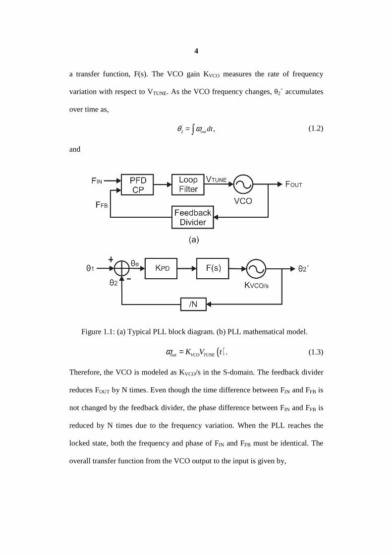
4
a transfer function, F(s). The VCO gain KVCO measures the rate of frequency
variation with respect to VTUNE. As the VCO frequency changes, θ2´ accumulates
over time as,
'2 ,outdtθ ω= ∫ (1.2)
and
( ).out VCO TUNEK V tω = (1.3)
Therefore, the VCO is modeled as KVCO/s in the S-domain. The feedback divider
reduces FOUT by N times. Even though the time difference between FIN and FFB is
not changed by the feedback divider, the phase difference between FIN and FFB is
reduced by N times due to the frequency variation. When the PLL reaches the
locked state, both the frequency and phase of FIN and FFB must be identical. The
overall transfer function from the VCO output to the input is given by,
Figure 1.1: (a) Typical PLL block diagram. (b) PLL mathematical model.

5
( ) ( )( )
'2
1
,PD VCO
PD VCO
NK K F ss
Ns K K F s
θθ
=+
(1.4)
and the transfer function from the feedback divider output to the input is given by,
( ) ( )( )
2
1
.PD VCO
PD VCO
K K F ss
Ns K K F s
θθ
=+
(1.5)
The transfer function exhibits low-pass characteristics. As θ1 changes slowly, θ2´
is able to track θ1 closely, and the phase variation of θ1 is inherited by θ2 and θ2´.
When θ1 changes rapidly, the PLL cannot respond fast enough to preserve the
phase alignment between FIN and FOUT. Therefore, the noise associated with the
input signal at low frequency offset is passed to the output un-attenuated while the
noise at high frequency offset is filtered.
1.2.1 Phase Frequency Detector and Charge Pump
The architecture of the typical PFD and the charge pump is shown in Figure
Figure 1.2: (a) PFD and current-mode charge pump. (b) PFD and charge
pump operating characteristics.

6
1.2(a). The PFD compares both the frequency and phase difference between the
input and the feedback signal, and generates two output signals UP and DN. The
relatively frequency and phase difference between θIN and θFB determine the
polarity and pulse-width of UP and DN. The polarity of UP and DN determines if
the charge pump current ICP is sourced or sink from the loop filter, and the pulse-
width of UP and DN determines the time-average magnitude of ICP. The variation
of the time-average charge pump current ICP with respect to the phase difference
between θIN and θFB is shown in Figure 1.2(b), where a linear relationship exists
under the ideal case. When θIN aligns with θFB, the average charge pump current is
zero. When θIN leads or lags θFB by 2π, the charge pump sources or sinks ICP from
the loop filter. As a result, KPD in Figure 1.1(b) is given by,
.2
CP
PD
IK
π= (1.6)
1.2.2 Loop Filter
The schematic of the current-mode passive loop filter is shown in Figure 1.3.
The charge pump current ICP is converted into VTUNE through the loop filter, and
Figure 1.3: Current-mode second-order passive loop filter.

7
the transfer function F(s) in Figure 1.1 is given by,
( ) ( )1
1 2 1 2
1.TUNE
CP
V sC RF s
I s sC C R C C
+= =+ +
(1.7)
The transfer function exhibits two poles and one zero. The PLL loop dynamics
can be conveniently set by adjusting the passive components values.
1.2.3 PLL Loop Dynamics
The open-loop transfer function of the PLL is given by,
( ) ( )( )
12
1 2 1 2
1( ) ,
2CP VCOVCO
loop PD
I K sC RKG s K F s
s s sC C R C Cπ+
= =+ +
(1.8)
The transfer function consists of three poles with two poles at DC. Therefore, this
type of PLL is also referred as Type-II. Due to the two poles at DC, the PLL is
unstable, and a compensation zero is required for stability by adding the resistor
Figure 1.4: Magnitude and phase response of the open-loop response.
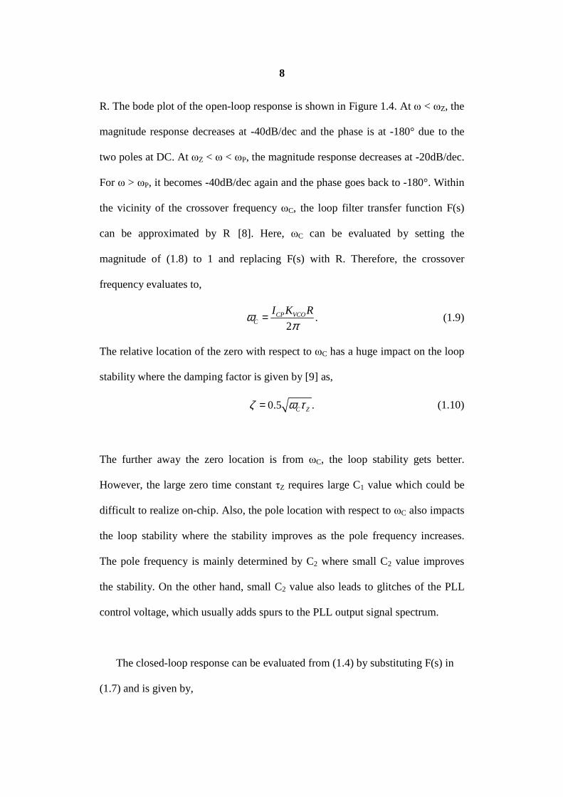
8
R. The bode plot of the open-loop response is shown in Figure 1.4. At ω < ωZ, the
magnitude response decreases at -40dB/dec and the phase is at -180° due to the
two poles at DC. At ωZ < ω < ωP, the magnitude response decreases at -20dB/dec.
For ω > ωP, it becomes -40dB/dec again and the phase goes back to -180°. Within
the vicinity of the crossover frequency ωC, the loop filter transfer function F(s)
can be approximated by R [8]. Here, ωC can be evaluated by setting the
magnitude of (1.8) to 1 and replacing F(s) with R. Therefore, the crossover
frequency evaluates to,
.2
CP VCOC
I K Rωπ
= (1.9)
The relative location of the zero with respect to ωC has a huge impact on the loop
stability where the damping factor is given by [9] as,
0.5 .C Zζ ω τ= (1.10)
The further away the zero location is from ωC, the loop stability gets better.
However, the large zero time constant τZ requires large C1 value which could be
difficult to realize on-chip. Also, the pole location with respect to ωC also impacts
the loop stability where the stability improves as the pole frequency increases.
The pole frequency is mainly determined by C2 where small C2 value improves
the stability. On the other hand, small C2 value also leads to glitches of the PLL
control voltage, which usually adds spurs to the PLL output signal spectrum.
The closed-loop response can be evaluated from (1.4) by substituting F(s) in
(1.7) and is given by,
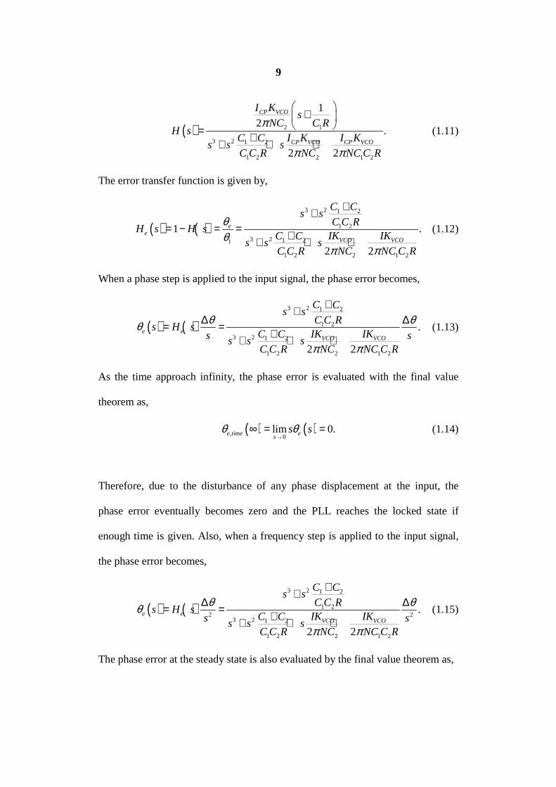
9
( ) 2 1
3 2 1 2
1 2 2 1 2
12
.
2 2
CP VCO
CP VCO CP VCO
I Ks
NC C RH s
I K I KC Cs s s
C C R NC NC C R
π
π π
+
=++ + +
(1.11)
The error transfer function is given by,
( ) ( )3 2 1 2
1 2
3 2 1 21
1 2 2 1 2
1 .
2 2
ee
VCO VCO
C Cs s
C C RH s H s
IK IKC Cs s s
C C R NC NC C R
θθ
π π
++= − = =
++ + + (1.12)
When a phase step is applied to the input signal, the phase error becomes,
( ) ( )3 2 1 2
1 2
3 2 1 2
1 2 2 1 2
.
2 2
e eVCO VCO
C Cs s
C C Rs H s
IK IKC Cs ss s sC C R NC NC C R
θ θθ
π π
++∆ ∆= =
++ + + (1.13)
As the time approach infinity, the phase error is evaluated with the final value
theorem as,
( ) ( ), 0lim 0.e time es
s sθ θ→
∞ = = (1.14)
Therefore, due to the disturbance of any phase displacement at the input, the
phase error eventually becomes zero and the PLL reaches the locked state if
enough time is given. Also, when a frequency step is applied to the input signal,
the phase error becomes,
( ) ( )3 2 1 2
1 22 2
3 2 1 2
1 2 2 1 2
.
2 2
e eVCO VCO
C Cs s
C C Rs H s
IK IKC Cs ss s sC C R NC NC C R
θ θθ
π π
++∆ ∆= =
++ + + (1.15)
The phase error at the steady state is also evaluated by the final value theorem as,
10
( ) ( ), 0lim 0e time es
s sθ θ→
∞ = = (1.16)
This result shows that the PLL is able to recover from any frequency step and
becomes locked again. Equations (1.14) and (1.16) show that the PLL is able to
reach the locked state subject to input frequency and phase offset.
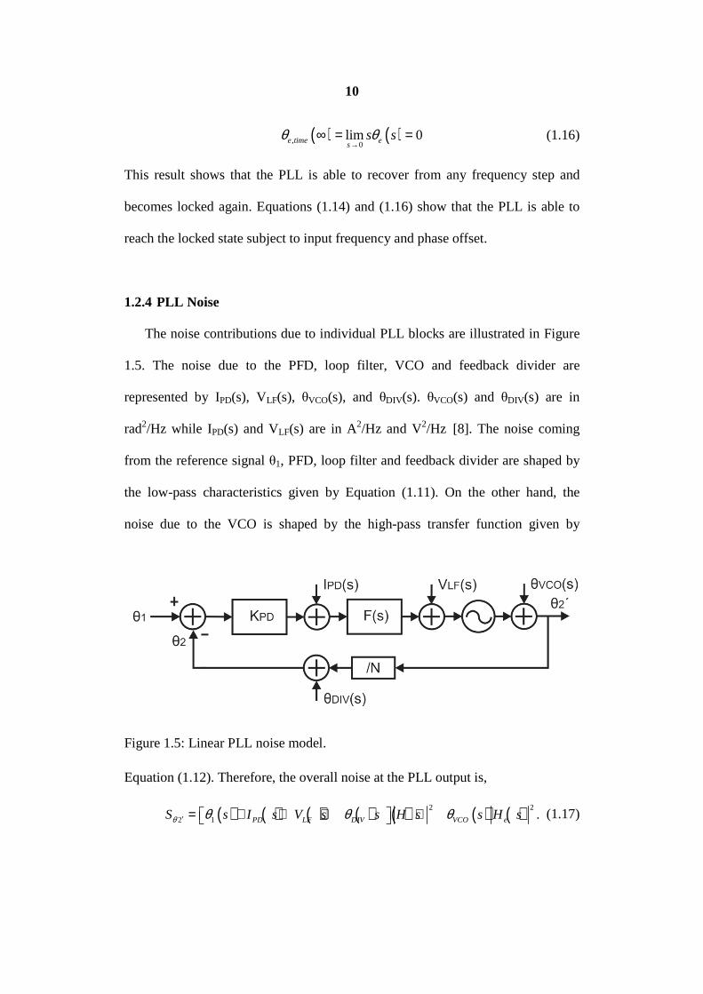
1.2.4 PLL Noise
The noise contributions due to individual PLL blocks are illustrated in Figure
1.5. The noise due to the PFD, loop filter, VCO and feedback divider are
represented by IPD(s), VLF(s), θVCO(s), and θDIV(s). θVCO(s) and θDIV(s) are in
rad2/Hz while IPD(s) and VLF(s) are in A2/Hz and V2/Hz [8]. The noise coming
from the reference signal θ1, PFD, loop filter and feedback divider are shaped by
the low-pass characteristics given by Equation (1.11). On the other hand, the
noise due to the VCO is shaped by the high-pass transfer function given by
Equation (1.12). Therefore, the overall noise at the PLL output is,
( ) ( ) ( ) ( ) ( ) ( ) ( )2 2
2 1 .PD LF DIV VCO eS s I s V s s H s s H sθ θ θ θ′ = + + + + (1.17)
Figure 1.5: Linear PLL noise model.

11
In general, the PLL output noise can be improved by decreasing the feedback
divider N, decreasing KVCO, decreasing RS in the loop filter, and increasing the
charge pump current. Also, reducing the phase noise of the VCO and the feedback
divider can also reduce PLL noise.
The PLL loop bandwidth also has an impact on the PLL noise performance.
PLL with lower bandwidth greatly attenuates the noise coming from the reference
signal but the majority of the VCO phase noise is passed to the VCO output. On
the other hand, PLL with higher bandwidth attenuates VCO phase noise more
effectively but the reference signal noise is unfiltered. Therefore, PLL loop
bandwidth is designed mainly based on noise requirement for different
applications. For frequency synthesis application, the PLL is driven by a crystal
oscillator with extremely high frequency purity. Therefore, the PLL bandwidth is
set much higher to suppress the VCO phase noise which usually dominates the
PLL output noise. The upper bound on the PLL bandwidth is limited by PLL loop
stability [10] where the loop bandwidth needs to be at least ten times less than the
reference signal frequency for the developed continuous model to be valid.
1.2.5 PLL Architecture
The two major PLL architectures are the integer-N PLL and fractional-N PLL
with advantages and disadvantages associated with each structure. The feedback
divider of the integer-N PLL in Figure 1.1 can only reduce the output frequency
by integer-N times as given by Equation (1.1). Therefore, the output frequency

12
resolution is limited by FIN, where FOUT can only be changed by FIN increment. In
order to improve the output frequency resolution, the reference frequency must
decrease, which requires narrow PLL loop bandwidth for stability reason as
described in the previous section. The drawbacks of narrow loop bandwidth
include slow transient settling time and poor VCO phase noise rejection. Also, the
feedback division ratio needs to increase, which degrades the PLL noise
performance. Narrow PLL loop bandwidth and slow settling time are highly
undesired traits for frequency synthesis applications.
To improve the PLL performance, the fractional-N PLL architecture is
proposed where the feedback division ratio can be any fractional value. The most
direct benefit of using a fractional feedback divider is that fine resolution at the
PLL output can be achieved at much higher reference frequency and PLL loop
bandwidth. The simplest way to achieve the fractional division is through the
dual-counter divider shown in Figure 1.6 [8]. The VCO output signal FOUT is sent
to a divider capable of dividing by N or N+1. Two other counters control if the
Figure 1.6: Dual-counter feedback divider.
13
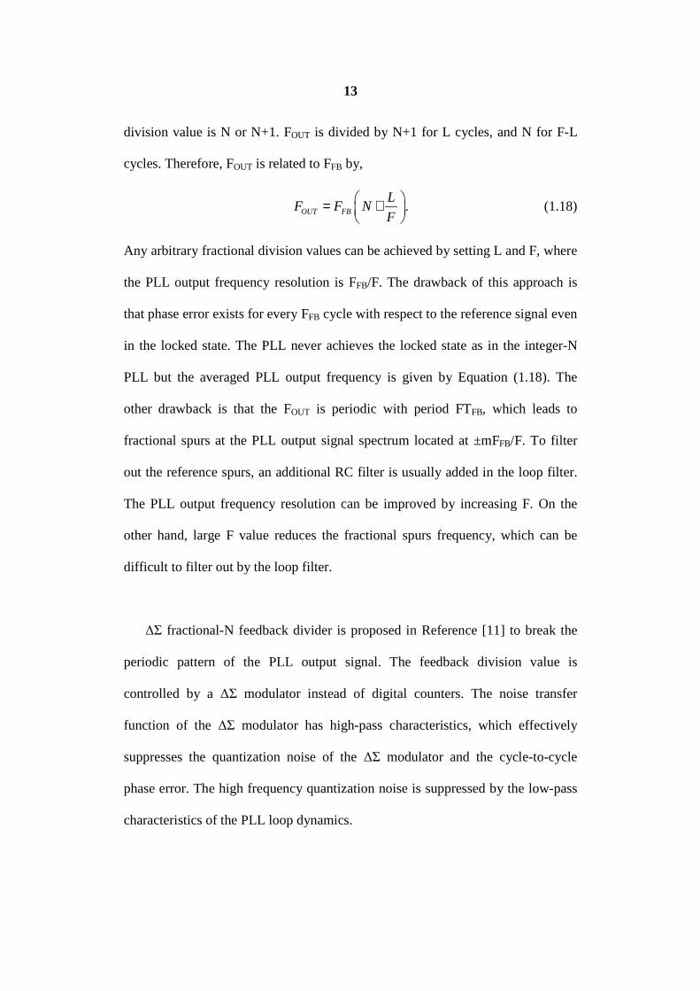
division value is N or N+1. FOUT is divided by N+1 for L cycles, and N for F-L
cycles. Therefore, FOUT is related to FFB by,
.OUT FB
LF F N
F = +
(1.18)
Any arbitrary fractional division values can be achieved by setting L and F, where
the PLL output frequency resolution is FFB/F. The drawback of this approach is
that phase error exists for every FFB cycle with respect to the reference signal even
in the locked state. The PLL never achieves the locked state as in the integer-N
PLL but the averaged PLL output frequency is given by Equation (1.18). The
other drawback is that the FOUT is periodic with period FTFB, which leads to
fractional spurs at the PLL output signal spectrum located at ±mFFB/F. To filter
out the reference spurs, an additional RC filter is usually added in the loop filter.
The PLL output frequency resolution can be improved by increasing F. On the
other hand, large F value reduces the fractional spurs frequency, which can be
difficult to filter out by the loop filter.
∆Σ fractional-N feedback divider is proposed in Reference [11] to break the
periodic pattern of the PLL output signal. The feedback division value is
controlled by a ∆Σ modulator instead of digital counters. The noise transfer
function of the ∆Σ modulator has high-pass characteristics, which effectively
suppresses the quantization noise of the ∆Σ modulator and the cycle-to-cycle
phase error. The high frequency quantization noise is suppressed by the low-pass
characteristics of the PLL loop dynamics.

14
1.3 LC-VCO Overview
The LC-VCOs are widely employed in wireless transceivers and frequency
synthesizers usually have the two structures as shown in Figure 1.7. The LC tank
consists of the on-chip integrated inductor and the varactor with tunable
capacitance implemented with M6-7. The Switching transistor M2-5 forms the
negative resistance to compensate for the series resistance loss of the integrated
inductor in order to sustain oscillation. Transistor M1 provides constant current to
the LC tank, where the oscillating amplitude is proportional to the drain current of
M1. The oscillating frequency is tunable by changing VTune, and the achievable
frequency tuning range depends on a number of factors including the oscillating
amplitude, varactor C-V characteristics and the parasitic capacitances associated
with M2-5.
Figure 1.7: (a) Top-biased PMOS LC-VCO. Top-biased
complementary LC-VCO.
15
1.3.1 Integrated Inductor
The on-chip integrated inductor is generally implemented with the top metal
layer available in the CMOS technology since:
(1) The top-metal layer has relatively low sheet resistance due to the extra
thickness of the metal layer.
(2) The top metal layer has the largest distance from the substrate therefore
the parasitic capacitances are much lower.
The inductance is designed with a spiral shape where the geometry of the inductor
has a huge impact on the inductance value. The inductance consists of two
components, the self-inductance of each metal strips and the mutual inductance
between the metal strips. Some key geometry parameters of the inductor include
the number of sides, the number of turns, the metal width, and the separation
distance between adjacent turns.
The figure-of-merit of an inductor is the quality factor which is defined as,
.S
LQ
R
ω= (1.19)
where, ω, L and RS are the signal frequency, inductance and series resistance of
the inductor [12]. To improve the inductor quality factor, some general guidelines
apply as:
(1) The number of sides of the inductor is maximized to improve the mutual
inductance between adjacent metal strips. As a result, the total inductance
increases for the same series resistance.
(2) The number of turns of the inductor needs to be set to an optimal value.
The quality factor improves as the number of turns increases since both

16
the inductance and the resistance increase with respect to the number of
turns where the rate of the inductance increase is larger than that of the
resistance due to the multiplicity of the mutual inductance increase. The
upper bound of the number of turns is limited by the required inductance
value in order to achieve the desired oscillating frequency.
(3) The metal width also needs to be optimized. Wide metal width is usually
required to decrease the metal sheet resistance. On the other hand, wide
metal also increase the parasitic capacitance with respect to the substrate.
Moreover, the metal resistance increases with respect to the frequency due
to the skin effect where the electrons only travel beneath the metal surface
at high frequency [13]. Therefore, increasing metal width will no longer
improve the metal sheet resistance.
(4) The separation distance between adjacent metal turns is minimized to
increase the mutual inductance.
Figure 1.8: Lumped model of on-chip inductor.
17
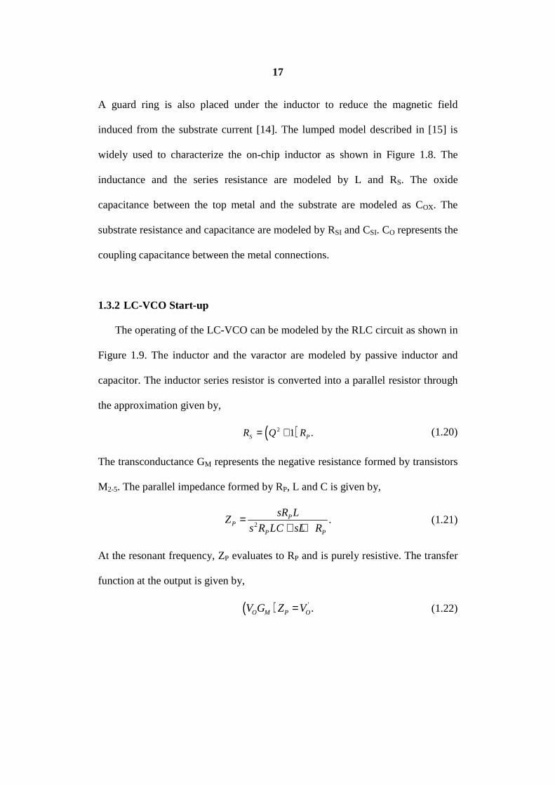
A guard ring is also placed under the inductor to reduce the magnetic field
induced from the substrate current [14]. The lumped model described in [15] is
widely used to characterize the on-chip inductor as shown in Figure 1.8. The
inductance and the series resistance are modeled by L and RS. The oxide
capacitance between the top metal and the substrate are modeled as COX. The
substrate resistance and capacitance are modeled by RSI and CSI. CO represents the
coupling capacitance between the metal connections.
1.3.2 LC-VCO Start-up
The operating of the LC-VCO can be modeled by the RLC circuit as shown in
Figure 1.9. The inductor and the varactor are modeled by passive inductor and
capacitor. The inductor series resistor is converted into a parallel resistor through
the approximation given by,
( )2 1 .S PR Q R= + (1.20)
The transconductance GM represents the negative resistance formed by transistors
M2-5. The parallel impedance formed by RP, L and C is given by,
2
.PP
P P
sR LZ
s R LC sL R=
+ + (1.21)
At the resonant frequency, ZP evaluates to RP and is purely resistive. The transfer
function at the output is given by,
( ) ' .O M P OV G Z V= (1.22)

18
If the following conditions are satisfied then,
'
1, 180 ,OM P M P
O
VG Z G Z
V= ≥ = °∡ (1.23)
oscillation at VO will sustain. This condition is the well-known Barkhausen
criterion used in system stability analysis. To ensure VCO start-up, GM of LC-
VCO is made at least two or three times larger than that of RP by increasing
transistor M2-5 aspect ratios.
Figure 1.9: Simplified LC-VCO model.
Figure 1.10: Simplified LC-VCO model.

19
1.3.3 LC-VCO Phase Noise
The LC-VCO phase noise is defined as the ratio of the noise power within
1Hz bandwidth at a frequency offset with respect to the carrier, and the carrier
power. The noise associated with RP is modeled by a current signal In,Rp as shown
in Figure 1.10, which enters the LC tank with the transfer function,
,
.1
O P
n Rp M P
V Z
I G Z=
− (1.24)
Therefore, the output noise power at a frequency offset ω+∆ω due to In,Rp is,
( )
( ) ( )2
22, .
1P
O n RpM P
ZV I
G Z
ω ωω ω
+ ∆= − + ∆
(1.25)
In,Rp is modeled by the thermal noise of the resistor RP. The phase noise is derived
by dividing the output noise power by the carrier power, and is given by,
( ) ( )2
2 2
4 11 .
4P
mm
kTRL F
A Q
ωωω
= +
(1.26)
where, A is the oscillating signal amplitude, ωm is the frequency offset, ω is the
Figure 1.11: Typical LC-VCO phase noise model.
20
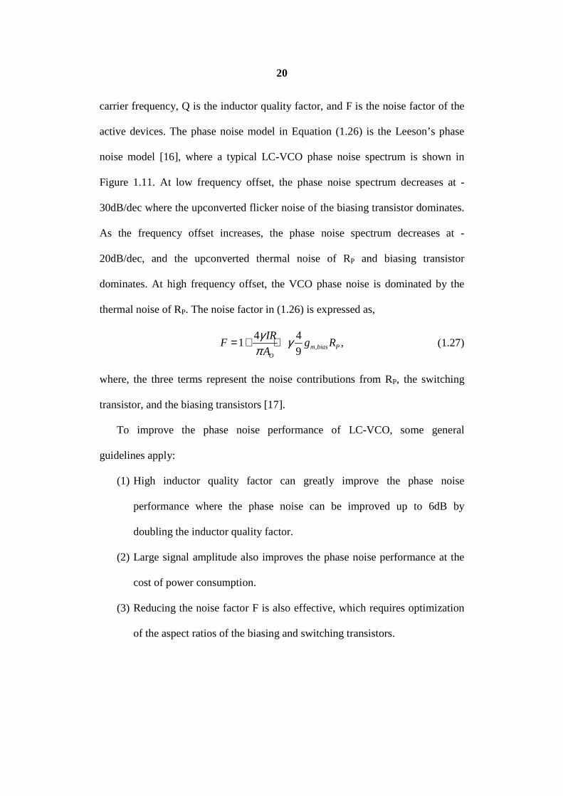
carrier frequency, Q is the inductor quality factor, and F is the noise factor of the
active devices. The phase noise model in Equation (1.26) is the Leeson’s phase
noise model [16], where a typical LC-VCO phase noise spectrum is shown in
Figure 1.11. At low frequency offset, the phase noise spectrum decreases at -
30dB/dec where the upconverted flicker noise of the biasing transistor dominates.
As the frequency offset increases, the phase noise spectrum decreases at -
20dB/dec, and the upconverted thermal noise of RP and biasing transistor
dominates. At high frequency offset, the VCO phase noise is dominated by the
thermal noise of RP. The noise factor in (1.26) is expressed as,
,
4 41 ,
9 m bias PO
IRF g R
A
γ γπ
= + + (1.27)
where, the three terms represent the noise contributions from RP, the switching
transistor, and the biasing transistors [17].
To improve the phase noise performance of LC-VCO, some general
guidelines apply:
(1) High inductor quality factor can greatly improve the phase noise
performance where the phase noise can be improved up to 6dB by
doubling the inductor quality factor.
(2) Large signal amplitude also improves the phase noise performance at the
cost of power consumption.
(3) Reducing the noise factor F is also effective, which requires optimization
of the aspect ratios of the biasing and switching transistors.

21
The oscillating signal amplitude variation with respect to the biasing current is
shown in Figure 1.12. When the biasing current is less than IOPT, the signal
amplitude increases linearly with respect to the bias current, where the VCO
operates in the current-limited region. The signal amplitude is eventually bounded
by the operating point of the switching transistors, and further increase of the
biasing current no longer increases the signal amplitude. The VCO operates in the
voltage-limited mode, where the signal amplitude stays constant with respect to
the biasing current. Therefore, for optimal phase noise without excessive power
consumption, IBIAS should be set within the vicinity of IOPT. The figure-of-merit
(FoM) of the LC-VCO is given by,
21
,m
FoML P
ωω
= ⋅ (1.28)
which accounts for the VCO phase noise, power consumption and frequency
offset. The FoM is convenient for comparing VCO performances operating at
different carrier frequencies.
Figure 1.12: Oscillating signal variation with respect to the biasing current.
22
1.3.4 LC-VCO Topology
The two common LC-VCO topologies shown in Figure 1.7 are widely used in
wireless and communication systems. For the same biasing current, the oscillating
signal amplitude of the complementary VCO is almost twice compared to the
signal amplitude of the PMOS VCO. Therefore, the complementary VCO is the
preferred choice for low power applications. As the biasing current increases, the
signal amplitude of the complementary VCO is limited by the switching
transistors. On the other hand, the signal amplitude of the PMOS VCO can grow
to a much larger value. Therefore, the PMOS VCO is the preferred choice if good
phase noise performance is the primary consideration.
1.4 PLL in Lock-In Amplifier
Other than the aforementioned three major applications of the PLL, there are a
number of other applications where PLL is employed, and one of these
applications is the lock-in amplifier (LIA). The LIAs are widely used systems in
physical and chemical sensing and materials spectroscopy applications [18]-[25].
LIAs aim to solve a common problem encountered in the data acquisition of weak
(small amplitude current or voltage) signals that are distorted by noisy
background signals. In short, LIAs improve the signal to noise ratio of the signal
and are the preferred choice in applications where the desired output signal is
usually embedded within considerable noise power and in many situations with
noise power many times more than that of the desired signal [3-5].

23
The function of the PLL in the LIA is similar to that in the wireless
transceivers. The PLL generates the reference signal with the same frequency as
the input signal. The mixer down-converts the input signal to DC based on the
reference signal. Since the input signal is within the kHz range, LC-VCO is not
feasible to integrate and ring-VCO is usually implemented.
1.5 Thesis Contributions and Organizations
The contributions of this dissertation are to improve LC-VCO and PLL
performance from the circuit perspective, and improve the overall performance of
the LIA in return. Four projects are undertaken and presented in the following
order:
Chapter 2 presents the design details of a CMOS optoelectronic LIA for
sensing and spectroscopy application. The design uses a phototransistor array to
convert the incident optical signals into electrical currents. The photocurrents are
then converted into voltage signals using a transimpedance amplifier for
subsequent convenient signal processing by the LIA circuitry. The noise and
signal distortions are suppressed with filters and PLL implemented in the LIA,
and the output DC voltage is directly proportionally to the input optical power.
In Chapter 3, an oscillation frequency linearization technique for LC-VCO
with an inversion-mode varactor is proposed. The linearity of the frequency
tuning curve is improved by linearization of C(V) characteristics of the inversion-

24
mode varactor. A new varactor configuration consisting of varactor units and
resistor divider network is proposed. The single-switch integrated LC-VCO with
the proposed varactor configuration is fabricated in TSMC 0.18µm CMOS
technology. The improvement of linearity of the frequency tuning curve has been
verified using mathematical models and measurement results.
Chapter 4 presents the design and development of a low-power LC-VCO with
improved phase noise performance by implementing a new capacitor divider
varactor configuration and a 2nd order notch filter. Also, this chapter presents a
new time-weighted approach to model the effective capacitance experienced by
the oscillating signal over the oscillation period.
In chapter 5, a general-purpose high-speed integrated LIA is designed, which
consists of the magnitude and phase measurement circuitry components to extract
the input signal magnitude and phase where the SNR can be as worse as -30dB.
The magnitude measurement circuitry relies on the band-pass filter and a current
integrator to generate the VMAG signal where VMAG is directly proportional to the
input signal amplitude. The phase measurement circuitry uses a low-bandwidth
PLL and current integrator to generate the VPH where VPH is directly proportional
to the phase difference between the input signal and the reference signal. The
designed LIA is fully integrated and requires no off-chip components.
The dissertation is concluded in Chapter 6.
25
CHAPTER 2: CMOS OPTOELECTRONIC LIA
In this chapter, a CMOS optoelectronic LIA for sensing and spectroscopy
application is presented. In the lock-in-amplification technique, the signal
obtained from the input/sensing interface is modulated at a known frequency. The
signal is multiplied with a known reference signal of the same frequency as the
input signal. The multiplied product signal is then down-converted to a low-
frequency signal from which the amplitude and phase of the desired signal is
extracted. To date, there have been many implementations of LIA in CMOS
technology. For example, in Johnson et al. [18], the LIA is used to monitor
exocytosis variation by measuring the changes in cell membrane capacitance. The
input signal was modulated by a pair of quadrature reference signals. The LIA
generated the full-wave rectification of the input signal where the DC component
is filtered out. The system operates at 1.5kHz. The input signal amplitude is at
50mV, and the output signal range is from 0.1V to 1V. In De Marcellis et al. [20],
a low-frequency LIA operating under 100Hz frequency is proposed. The input
signal is first processed by a low-noise amplifier (LNA) and a band-pass filter.
Then, the signal is down-converted to the baseband by a mixer where the DC
component was filtered out by a low-pass filter. The design was implemented in
CMOS 0.35µm technology where the intrinsic gain of the LIA was measured to
be 5691V/V. In Gnudi et al. [21], the structure of the proposed LIA is similar to
the structure described in [20]. The design was fabricated in CMOS 0.7µm
technology, and consumed 25mW static power. The system operated at 20kHz,

26
and was capable of extracting signals as small as 100nV from the ambient noise.
In Azzolini et al. [22], the LIA was used to detect low-level signals in
magnetically excited resonant structures. The input signal was modulated by a
pair of quadrature signals where the reference signal was generated by a PLL. The
design was fabricated in CMOS 0.35µm technology, and consumed 110mW static
power. That system was capable of extracting signals of 1µV at 30kHz.
In this Chapter, we describe the design and development of a low-power
monolithically integrated optoelectronic LIA implemented in TSMC 0.35µm
CMOS technology. Optoelectronic LIAs are indispensible in optical materials
spectroscopy and can be very useful in optical (luminescence)-based biological
and chemical sensing. The developed LIA includes a high gain photo-transistor
array to convert the incident optical signals into electrical current signals. The
photocurrent is then amplified and converted into a voltage signal by a
transimpedance amplifier which is then processed by the LIA circuitry. Here, we
focus on luminescence intensity monitoring applications where we aim to extract
only the amplitude of the input signal. Thus, for the aforementioned specific
application, we propose a new architecture that does not require an external
reference signal since the reference signal is generated internally using a PLL. We
examined the functionality of the LIA using a LED as the optical source. This is
done since most low-power optical sensors prefer the use of an LED as the
excitation source. The proposed LIA consumes an average power of 12.79mW
with 3.3V power supply, and its operating frequency range is from 13kHz to
27
25kHz. This frequency bandwidth is selected since it is the optimum range in
many sensing and spectroscopy applications [26]-[28].
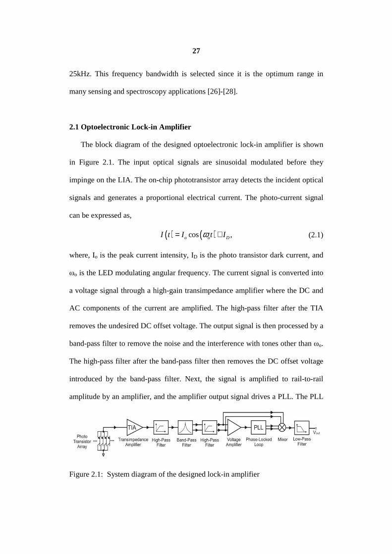
2.1 Optoelectronic Lock-in Amplifier
The block diagram of the designed optoelectronic lock-in amplifier is shown
in Figure 2.1. The input optical signals are sinusoidal modulated before they
impinge on the LIA. The on-chip phototransistor array detects the incident optical
signals and generates a proportional electrical current. The photo-current signal
can be expressed as,
( ) ( )cos ,o o DI t I t Iω= + (2.1)
where, Io is the peak current intensity, ID is the photo transistor dark current, and
ωo is the LED modulating angular frequency. The current signal is converted into
a voltage signal through a high-gain transimpedance amplifier where the DC and
AC components of the current are amplified. The high-pass filter after the TIA
removes the undesired DC offset voltage. The output signal is then processed by a
band-pass filter to remove the noise and the interference with tones other than ωo.
The high-pass filter after the band-pass filter then removes the DC offset voltage
introduced by the band-pass filter. Next, the signal is amplified to rail-to-rail
amplitude by an amplifier, and the amplifier output signal drives a PLL. The PLL
Figure 2.1: System diagram of the designed lock-in amplifier
28
provides a single tone at ωo with very small side-bands associated with ωo. As a
result, the PLL output spectrum resembles that of a band-pass filter with a very
high quality factor. The PLL output and the output signal after the second high-
pass filter are sent to a mixer. Since the PLL output side-band magnitudes are
very small, the noise power down-converted to the base-band is greatly reduced.
The mixer output signal can be expressed as,
( ) ( )cos 2 ,o o oV t I A I A tω= + (2.2)
where, A is the accumulated gain of the TIA, high-pass filter, band-pass filter, and
the mixer. V(t) consists of two tones located at the DC and 2ωo, respectively. A
low-pass filter is added after the mixer to remove the tone at 2ωo. Therefore, the
low-pass filter output signal, Vout (which is a dc voltage) is directly proportional to
the photo-current Io, where Io is proportional to the incident optical power. The
rest of this section describes the operation of each functional block in details.
2.1.1 Photo-transistor Array
The incident light is detected by an 11 × 18 phototransistor array. The
microphotograph of an array of six photo-transistor pixels is shown in Figure 2.2.
The area of each photo-transistor is 35µm × 35µm, and the overall area of the
photo-transistor array is 400µm × 640µm. The structure of the photo-transistor
pixel is similar to a bipolar junction transistor formed by P-active(emitter) / N-
well(base) / P-substrate(collector). The phototransistor is designed so that all of
the emitter terminals are connected to the input of the TIA, and the collector
terminals are connected to the ground. This vertical phototransistor structure has

29
demonstrated good responsively in the visible region of the electromagnetic
spectrum [26]-[28]. The bandwidth of the photo transistors is few hundred kilo-
hertz which covers the intended operating frequency range of the proposed LIA.
The vertical phototransistor architecture can produce currents that are several
times larger than a comparable sized photodiode which is required for detecting
low amplitude luminescence signals in sensing and spectroscopy [27][28].
2.1.2 Transimpedance Amplifier (TIA)
The TIA serves the purpose of converting the generated photo-current signal
I in into a voltage signal Vout. The circuit schematic is shown in Figure 2.3. The
bias voltages are provided off-chip. M3 and M4 are stacked to increase the TIA
transimpedance. The output DC voltage is forced to be approximately equal to
Vbx through replica biasing circuitry. The amplifier used in the replica biasing
circuitry is a standard 5-transistors differential to single-ended configuration. The
simulated performance of the TIA demonstrated large trans-impedance (120dBΩ),
good linearity, and relatively low noise (7.878pA/Hz ). The transimpedance is
approximated by,
Figure 2.2: Microphotograph of a single photo-transistor pixel.

30
2 2
2 2
( ) ,out m o
in gs m
V g rs
I sC g=
+ (2.3)
where, the low-frequency trans-impedance is ro2, and the bandwidth is gm2/Cgs2.
ro2 can be enlarged by increasing the aspect ratio of M2 at the cost of linearity,
noise performance and power consumption. The simulated TIA bandwidth is
303.5kHz, which exceeds the targeted operating range of 13kHz to 25kHz.
2.1.3 High-Pass Filter
The photo-transistor output currents include a DC and an AC component
where both components are amplified by the TIA. While the AC component does
not affect the output DC voltage, the DC component leads to an undesired DC
offset voltage at the output which imposes an unintended biasing voltage on the
downstream signal processing stages. Therefore, a high-pass filter is added after
the TIA to remove the undesired DC offset voltage. The schematic of the
designed high-pass filter is shown in Figure 2.4(a). This topology is taken from
Figure 2.3: Circuit schematic of the TIA. Transistor sizes: W1 = 50µm, W2 = 40µm, W3,4 = 200µm, L1-4 = 8µm. Vb1 = Vb2= Vbx = 1.6V, Vb3=1.2V.

31
[29] and consists of two operational-transconductance amplifiers (OTAs) and two
capacitors C1 and C2. The capacitors are implemented on chip. The schematic of
the OTAs is shown in Figure 2.4(b). The positive, negative and output terminals
of Gm2 form the unity-gain feedback configuration such that Vout follows Vc1. Gm1
and C1 are added on top of this configuration to increase the order of the filter by
one. Since, Vout follows Vc1, Vout also follows Vb1. Therefore, the output DC
voltage of the high-pass filter is set by Vb1. The input to output transfer function
is,
2
2 2 1 2
2 1 2
( ) .out
m m min
v ss
g g gv s sC C C
=+ +
(2.4)
Therefore, the pass-band gain is unity. The design challenge is to ensure that
the 3-dB bandwidth is lower than the smallest signal frequency to be detected
while the capacitor values are relatively small. To further reduce the bandwidth,
Gm1 and Gm2 are kept small. The simulated bandwidth is 7.34kHz which is less
than the targeted operating range of 13kHz to 25kHz when C1 and C2 are 10pF
Figure 2.4: (a) Circuit schematic of the high-pass filter. (b) Circuit schematic of the OTAs. Transistor sizes: W1 = 1µm, W2,3 = 500nm, W4,5 = 1.5µm, W6,7 = 800nm, L1-7 = 10.5µm. Vb1 = 1.6V, Vb2=0.45V.

32
and 1pF, respectively. The simulated output power spectral density at 20kHz is
403.4nV/ Hz .
2.1.4 Band-Pass Filter
The purpose of the band-pass filter is to remove the noise and the interference
associated with the signal to be detected. The topology of the band-pass filter is
shown in Figure 2.5(a), which consists of four OTAs and four capacitors. The
capacitors are provided on-chip. The band-pass filter converts the input signal
(V in) into a pair of differential output signals. Vref is a dc biasing voltage which
equals to Vb1 in Figure 2.4(a). The schematic of the OTA is shown in Figure
Figure 2.5: (a) Circuit schematic of the band-pass filter. (b) Circuit schematic of the OTAs. W1,2 = 0.9µm, W3,4 = 1.5µm, W5,6 = 1µm, W7 = 2.7µm, W8,9 = 8µm, W10-13 = 2µm, W14,15 = 4µm, L1-7 = 7µm, L8-15 = 0.35µm. Vb1 = 1.2V, Vb2=0.5V, Vb3 = Vbx=1.6V.

33
2.5(b), and the topology is taken from [30]. All the biasing voltages are provided
off-chip. The common-mode feedback (CMFB) circuitry sets the output dc
operating point to Vbx and reduces common-mode output voltage fluctuations
through negative feedback. The characteristic transfer function of the band-pass
filter is,
1
1
2 2 3 4
1 1 2
( ) ,
m
out
m m min
gs
v Cs
g g gv s sC C C
=+ +
(2.5)
and the center frequency and the quality factor are,
3 4
1 2
,m mo
g g
C Cω = (2.6)
and
3 1
2 2
.m
m
g CQ
g C= (2.7)
The design challenge of the band-pass filter is to pinpoint the center frequency
within the required operating frequency range without using unreasonably large
capacitors while maintaining a good quality factor. According to Equations (2.6)
and (2.7), the center frequency can be decreased by reducing gm3gm4 and enlarging
Figure 2.6: Simulated frequency response of the band-pass filter at different center frequencies.
34
C1C2 while the quality factor can be improved by increasing the ratio of C1 to C2
and gm3 to gm2. The OTA trans-conductance can be adjusted by varying the
biasing voltages and transistor aspect ratios. The transistor sizes shown in Figure
2.5(b) are that of gm1. The transistor sizes in gm2-4 and the biasing voltages are
adjusted to achieve the desired center frequency and quality factor where gm1 =
5gm2 = gm3 = gm4.The simulated frequency response at the center frequencies of
12.8kHz, 16.5kHz, 21.1kHz, and 26.8kHz is shown in Figure 2.6. The measured
quality factor is approximately 10, where C1 and C2 are 10pF and 1pF,
respectively. The simulated output power spectral density at 20kHz is simulated
to be 89.99 nV/Hz .
2.1.5 Phase-Locked Loop
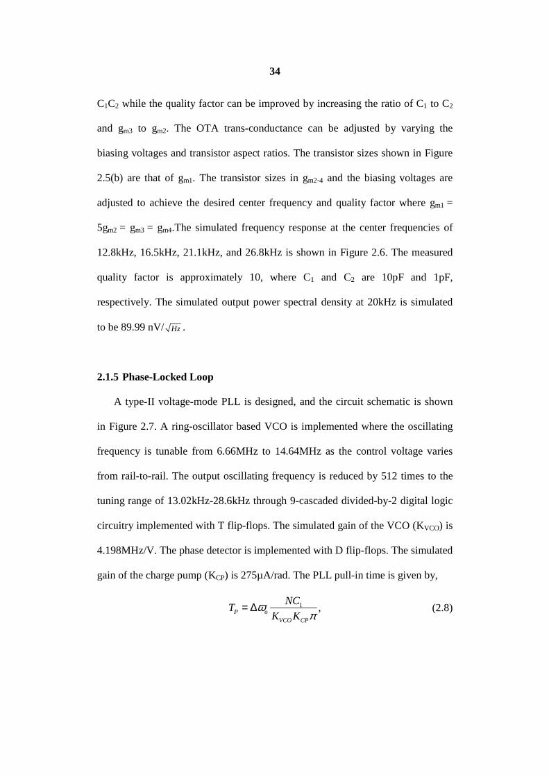
A type-II voltage-mode PLL is designed, and the circuit schematic is shown
in Figure 2.7. A ring-oscillator based VCO is implemented where the oscillating
frequency is tunable from 6.66MHz to 14.64MHz as the control voltage varies
from rail-to-rail. The output oscillating frequency is reduced by 512 times to the
tuning range of 13.02kHz-28.6kHz through 9-cascaded divided-by-2 digital logic
circuitry implemented with T flip-flops. The simulated gain of the VCO (KVCO) is
4.198MHz/V. The phase detector is implemented with D flip-flops. The simulated
gain of the charge pump (KCP) is 275µA/rad. The PLL pull-in time is given by,
1 ,P oVCO CP
NCT
K Kω
π= ∆ (2.8)
35
where, ∆ωo is the change in input frequency [31]. Therefore, for a 100ms pull-in
time and 1kHz frequency hopping, C1 is set to 0.22µF. The loop filter transfer
function is given by,
( ) ( )1
21 2 1 2
1.C
CP
V sRCs
I s RC C s C C
+=+ +
(2.9)
The zero (ωZ) locates at 1/RC1, and relates to the natural frequency (ωn) and
damping ratio (ζ) as,
,2
n
Z
ωζω
= (2.10)
where, ωn is given by,
1
.VCO CPn
K K
NCω = (2.11)
By setting ζ to 0.7 for optimal damping ratio and settling time, R is calculated to
be 5.69kΩ from ωZ. C2 is set to 30% of C1 as a general rule of thumb. R, C1 and
C2 are off-chip components during chip testing. The simulated PLL parameters
are summarized in Table 2.1.
Figure 2.7: Circuit schematic of the PLL. Transistor sizes: W1,2 = 4µm, W3 = 8µm, W4,5 = 4µm, W6 = 12µm, W7 = 192µm, W8 = 48µm, W9 = 3µm, L1-9 = 0.35µm.
36
Table 2.1: PLL performance summary
2.1.6 Mixer
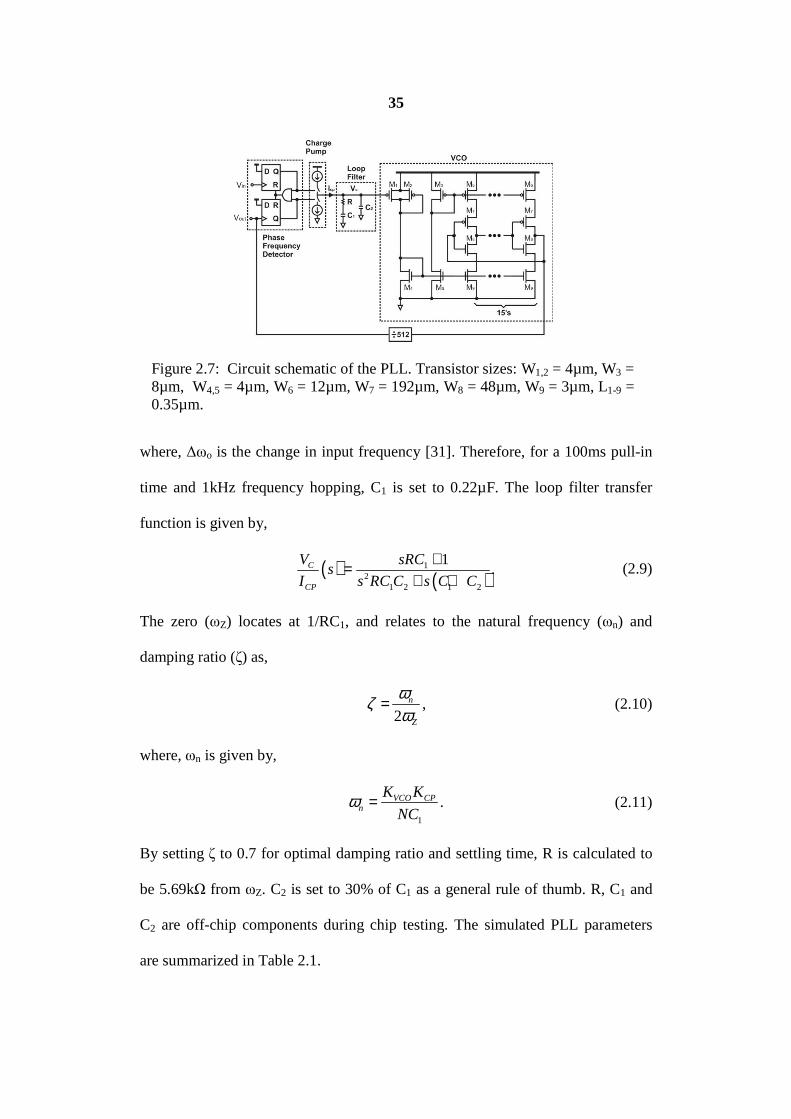
The mixer down-converts its input signal to DC by multiplying the local-
oscillator (LO) signal and the input signal where the two signals have the same
frequency. The schematic of the mixer is shown in Figure 2.8. Unlike Gilbert-cell
based mixer topology, the current source at the bottom is removed to increase the
headroom at the output. The biasing voltage is provided off-chip. The output
power spectral density at 20kHz is simulated to be 77.78 nV/ Hz .
Type Integer-N, Type-II Reference Frequency 20kHz VCO Tuning Range 13.02kHz-28.6kHz VCO Phase Noise (12.6MHz Center Freq.) -101.7dBc/Hz at 10kHz Power Consumption 5.22mW
Figure 2.8: Circuit schematic of the mixer. Transistor sizes: W1,2 = 1.95µm, W3-6 = 5.5µm, W7,8 = 5µm, L1-8 = 0.35µm. Vb = 1.52V.

37
2.1.7 Low-Pass Filter
The low-pass filter after the mixer removes the tone located at 2ωo. The
circuit schematic of the low-pass filter is shown in Figure 2.9. The topology is
taken from [29], and the schematic of the OTAs is the same as that of the high-
pass filter. The transfer function from the input to the output is given by,
1 2
1 2
2 2 1 2
2 1 2
( ) .
m m
out
m m min
g g
v C Cs
g g gv s sC C C
=+ +
(2.12)
The pass-band gain is unity, and the bandwidth should be small enough so
that the tone at 2ωo can be effectively removed. The simulated bandwidth of the
low-pass filter is 1.434kHz when C1 and C2 are 10pF and 5pF, respectively. Both
capacitors are implemented on-chip. The simulated output power spectral density
at 20kHz is 81.25 nV/Hz .
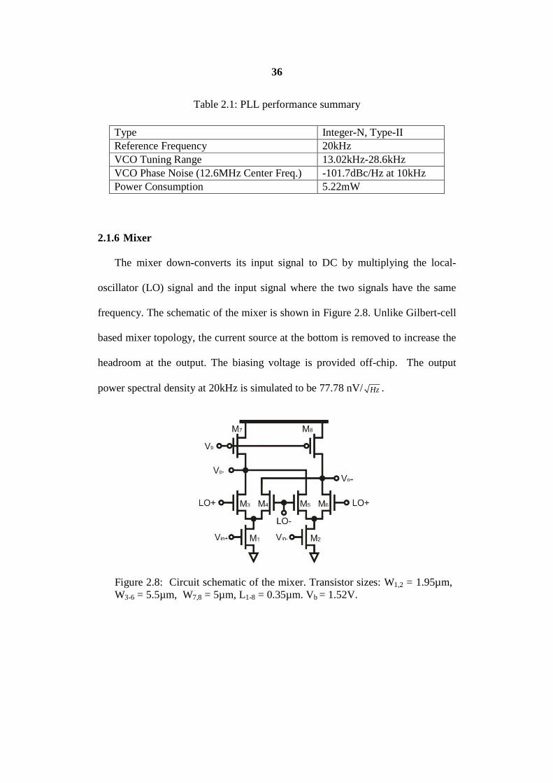
2.2 Experimental Measurements and Discussion
The designed lock-in amplifier is fabricated in TSMC CMOS 0.35µm
technology, and the die photo is shown in Figure 2.10. Only the phototransistor
Figure 2.9: Circuit schematic of the low-pass filter.

38
array is visible in the micrograph as the rest of the chip is covered by metal layer
to prevent noise due to interference of optical signals with the circuitry. The
optical responsivity of the photo-transistors and the TIA in the visible
electromagnetic spectrum are measured. A Xenon arc lamp is used as the white
light source. A monochromator is used to control the output light wavelength
where a partial spectrum of visible light (470nm to 690nm wavelength) is
synthesized. The power of the light is measured by an optical power meter. Figure
2.11 shows the TIA output voltage normalized with respect to the measured
optical power as a function of the wavelength. The photo-transistors demonstrate
maximum responsivity when they are excited by the orange wavelength (λ =
650nm), and least responsivity when they are excited by the blue wavelength (λ =
470nm wavelength). As a result, a blue LED is used in the subsequent
measurements to test the robustness of the system. Also, most of the luminescence
sensors emit in the wavelength between green and orange wavelength where the
system is most responsive [27][28].
Figure 2.10: Die photo of the lock-in amplifier.

39
The VCO tuning range is measured with respect to the control voltage as
shown in Figure 2.12. The frequency tuning range is from 32kHz to 13kHz as the
control voltage is swept from rail-to-rail which covers the intended frequency
operating range. The PLL phase noise is also measured, and the output spectrum
is shown in Figure 2.13, where the phase noise is measured as -58dBc/Hz at
100Hz offset.
A blue LED is used as the input light source and is driven by a function
generator at 20kHz. The DC offset voltage used to drive the LED is set to 2.2V,
2.525V, and finally to 2.85V in three steps while maintaining the same AC
amplitude such that the average optical power incident on the LIA is increased to
Figure 2.12: Measured VCO frequency with respect to the control voltage.
Figure 2.11: Responsivity of the phototransistor array and the TIA when excited by visible light.

40
67µW, 75µW, and 82µW, respectively. The measured lock-in amplifier DC
output voltages (shown in Figure 2.14) at these optical powers are 1.2V, 1.9V,
and 2.6V, respectively.
The lock-in amplifier output voltage versus the input optical power is shown
in Figure 2.15 which shows good linearity. The sensitivity is measured to be
approximately 100mV/µW (incident optical power). Strong interference is
introduced intentionally to the input signal to verify the robustness of the system
where the input signal of 20kHz is amplitude-modulated by another signal of
21kHz with 50% modulation depth. The measured output voltage versus the input
optical power is shown in Figure 2.15, where a linear relationship is preserved but
the sensitivity is reduced to 34mV/µW. The measured relationship when the
interference is changed to 100kHz and 50% modulation depth is also shown in
Figure 2.15, where the sensitivity is improved to 65mV/µW. It is worth
Figure 2.13: Measured PLL phase noise.
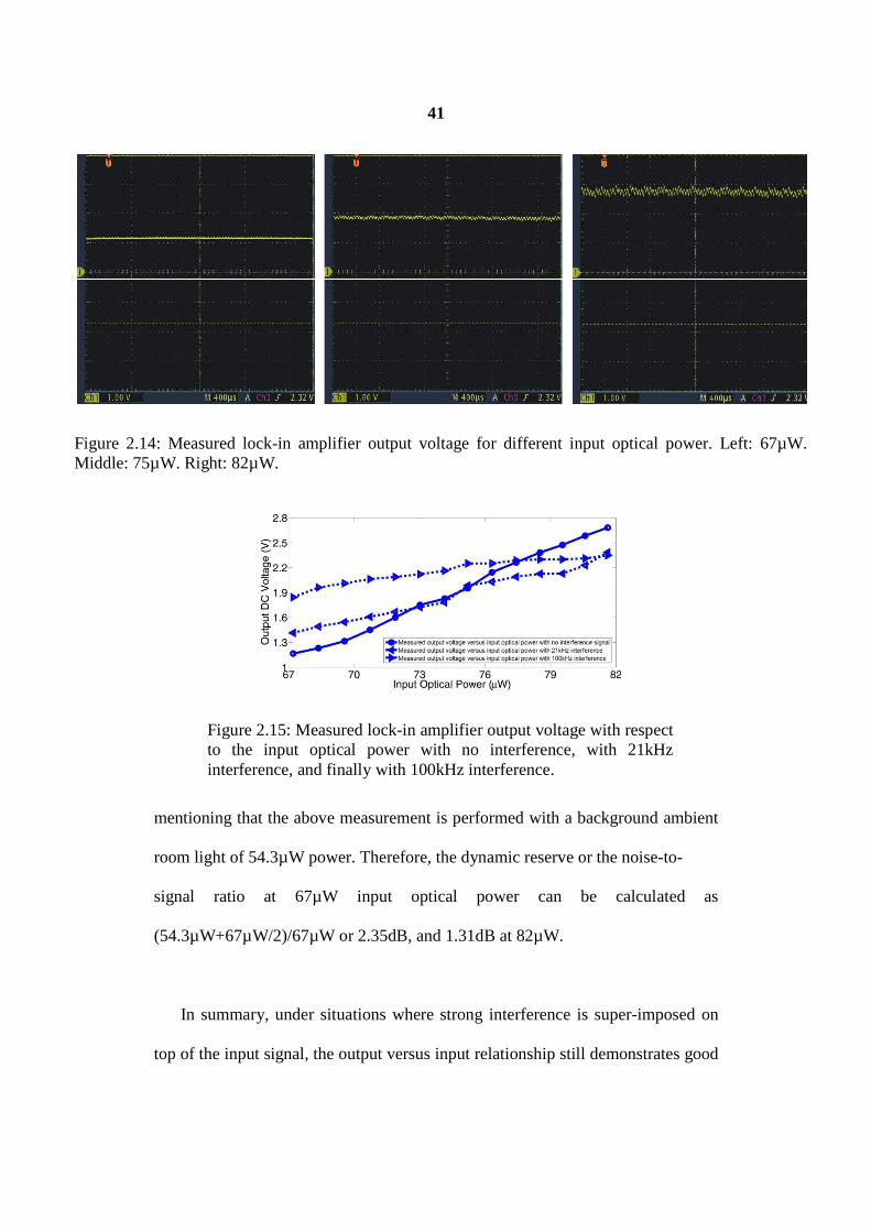
41
mentioning that the above measurement is performed with a background ambient
room light of 54.3µW power. Therefore, the dynamic reserve or the noise-to-
signal ratio at 67µW input optical power can be calculated as
(54.3µW+67µW/2)/67µW or 2.35dB, and 1.31dB at 82µW.
In summary, under situations where strong interference is super-imposed on
top of the input signal, the output versus input relationship still demonstrates good
Figure 2.15: Measured lock-in amplifier output voltage with respect to the input optical power with no interference, with 21kHz interference, and finally with 100kHz interference.
Figure 2.14: Measured lock-in amplifier output voltage for different input optical power. Left: 67µW. Middle: 75µW. Right: 82µW.
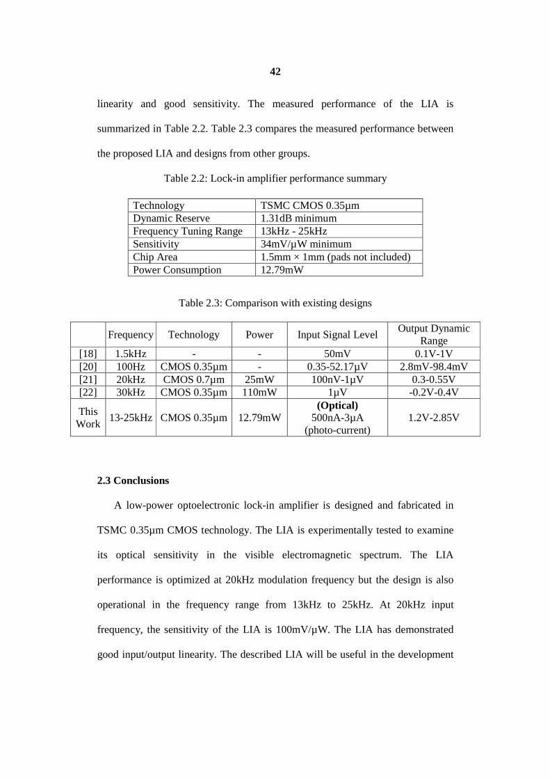
42
linearity and good sensitivity. The measured performance of the LIA is
summarized in Table 2.2. Table 2.3 compares the measured performance between
the proposed LIA and designs from other groups.
Table 2.2: Lock-in amplifier performance summary
Table 2.3: Comparison with existing designs
Frequency Technology Power Input Signal Level Output Dynamic
Range [18] 1.5kHz - - 50mV 0.1V-1V [20] 100Hz CMOS 0.35µm - 0.35-52.17µV 2.8mV-98.4mV [21] 20kHz CMOS 0.7µm 25mW 100nV-1µV 0.3-0.55V [22] 30kHz CMOS 0.35µm 110mW 1µV -0.2V-0.4V
This Work
13-25kHz CMOS 0.35µm 12.79mW (Optical)
500nA-3µA (photo-current)
1.2V-2.85V
2.3 Conclusions
A low-power optoelectronic lock-in amplifier is designed and fabricated in
TSMC 0.35µm CMOS technology. The LIA is experimentally tested to examine
its optical sensitivity in the visible electromagnetic spectrum. The LIA
performance is optimized at 20kHz modulation frequency but the design is also
operational in the frequency range from 13kHz to 25kHz. At 20kHz input
frequency, the sensitivity of the LIA is 100mV/µW. The LIA has demonstrated
good input/output linearity. The described LIA will be useful in the development
Technology TSMC CMOS 0.35µm Dynamic Reserve 1.31dB minimum Frequency Tuning Range 13kHz - 25kHz Sensitivity 34mV/µW minimum Chip Area 1.5mm × 1mm (pads not included) Power Consumption 12.79mW

43
of portable optical spectroscopy instrumentation and field-usable optical based
biological and chemical sensors.
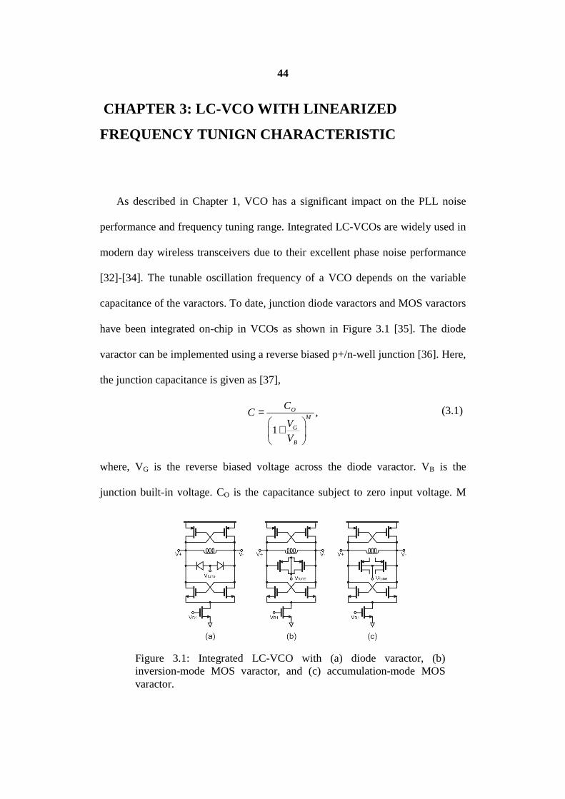
44
CHAPTER 3: LC-VCO WITH LINEARIZED
FREQUENCY TUNIGN CHARACTERISTIC
As described in Chapter 1, VCO has a significant impact on the PLL noise
performance and frequency tuning range. Integrated LC-VCOs are widely used in
modern day wireless transceivers due to their excellent phase noise performance
[32]-[34]. The tunable oscillation frequency of a VCO depends on the variable
capacitance of the varactors. To date, junction diode varactors and MOS varactors
have been integrated on-chip in VCOs as shown in Figure 3.1 [35]. The diode
varactor can be implemented using a reverse biased p+/n-well junction [36]. Here,
the junction capacitance is given as [37],
,
1
OM
G
B
CC
V
V
=
+
(3.1)
where, VG is the reverse biased voltage across the diode varactor. VB is the
junction built-in voltage. CO is the capacitance subject to zero input voltage. M
Figure 3.1: Integrated LC-VCO with (a) diode varactor, (b) inversion-mode MOS varactor, and (c) accumulation-mode MOS varactor.

45
depends on the junction doping profile [8]. As mentioned in [8], the disadvantages
associated with the diode varactor include limited control voltage range due to the
required voltage headroom to maintain the reverse biasing condition for the diode,
and reduced oscillation frequency tuning range due to the large parasitic
capacitance between the n-well and p-substrate.
The other approach to implement an on-chip varactor is to use metal-oxide
semiconductor (MOS) field-effect transistors (FETs). Two types of MOS
varactors have been implemented, the inversion-mode and accumulation-mode
varactors [38]. The inversion-mode varactor is implemented by connecting its
source and the drain of a MOSFET together as one capacitor terminal, and using
the gate as the other capacitor terminal. Here, the substrate is tied to VDD and thus
the transistor cannot enter the accumulation mode and the frequency tuning range
is enlarged [35]. In this case, the operation mode of the transistor changes
between the inversion mode and the depletion mode with respect to the voltage
variation across the varactor. The accumulation-mode varactor is implemented by
using the n-well as one capacitor terminal and the FET gate as the other capacitor
terminal. In this case, the operation mode of the transistor changes between the
accumulation mode and depletion mode. As the substrate is connected to a
variable tuning voltage, the accumulation-mode varactor is more susceptible to
latch-up [36]. The transition slope between the maximum and minimum
capacitances is steeper for the inversion-mode varactor, so the linear range of the
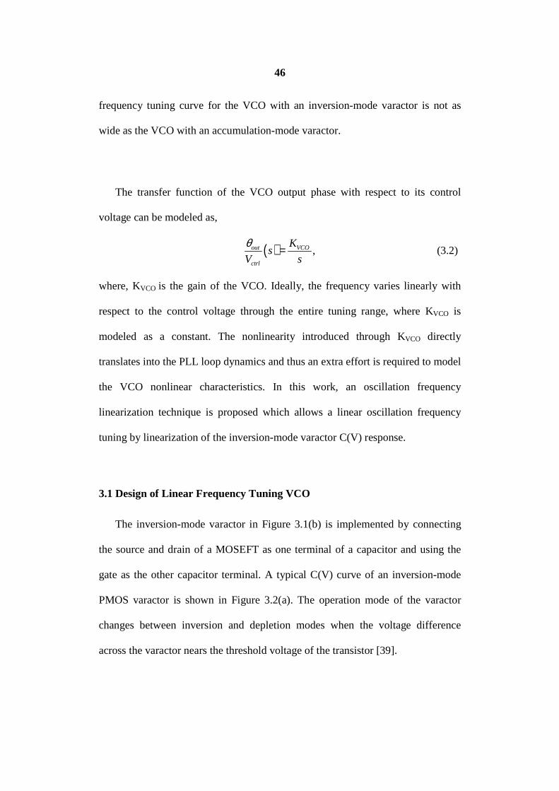
46
frequency tuning curve for the VCO with an inversion-mode varactor is not as
wide as the VCO with an accumulation-mode varactor.
The transfer function of the VCO output phase with respect to its control
voltage can be modeled as,
( ) ,out VCO
ctrl
Ks
V s
θ = (3.2)
where, KVCO is the gain of the VCO. Ideally, the frequency varies linearly with
respect to the control voltage through the entire tuning range, where KVCO is
modeled as a constant. The nonlinearity introduced through KVCO directly
translates into the PLL loop dynamics and thus an extra effort is required to model
the VCO nonlinear characteristics. In this work, an oscillation frequency
linearization technique is proposed which allows a linear oscillation frequency
tuning by linearization of the inversion-mode varactor C(V) response.
3.1 Design of Linear Frequency Tuning VCO
The inversion-mode varactor in Figure 3.1(b) is implemented by connecting
the source and drain of a MOSEFT as one terminal of a capacitor and using the
gate as the other capacitor terminal. A typical C(V) curve of an inversion-mode
PMOS varactor is shown in Figure 3.2(a). The operation mode of the varactor
changes between inversion and depletion modes when the voltage difference
across the varactor nears the threshold voltage of the transistor [39].
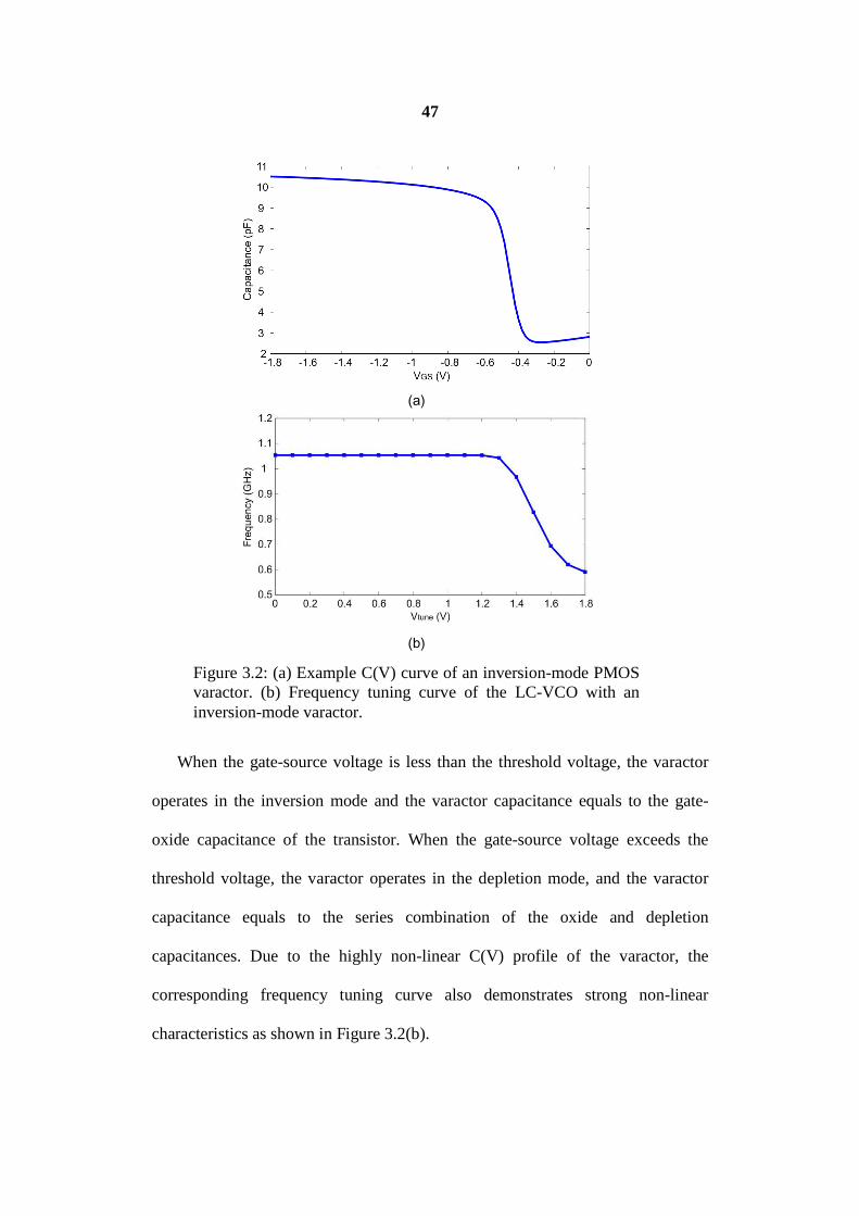
47
When the gate-source voltage is less than the threshold voltage, the varactor
operates in the inversion mode and the varactor capacitance equals to the gate-
oxide capacitance of the transistor. When the gate-source voltage exceeds the
threshold voltage, the varactor operates in the depletion mode, and the varactor
capacitance equals to the series combination of the oxide and depletion
capacitances. Due to the highly non-linear C(V) profile of the varactor, the
corresponding frequency tuning curve also demonstrates strong non-linear
characteristics as shown in Figure 3.2(b).
(a)
(b)
Figure 3.2: (a) Example C(V) curve of an inversion-mode PMOS varactor. (b) Frequency tuning curve of the LC-VCO with an inversion-mode varactor.
48
When the tuning voltage is less than 1.2V, the varactor operates in the
depletion mode and the oscillation frequency stays constant. The effective
capacitance experienced by the oscillation signal over the oscillation cycle does
not change and thus the oscillation frequency is invariant with respect to the
tuning voltage. When the tuning voltage exceeds 1.2V, the effective capacitance
experienced by the oscillation signal equals to the mix of oxide and depletion
capacitances, where the oscillation signal drives the varactor into inversion mode
for a portion of the oscillation period, and depletion mode for the rest of the
period. The higher the tuning voltage, the more time the varactor spends in the
inversion mode. Therefore, the effective capacitance increases with respect to the
tuning voltage and, thus, the oscillation frequency starts to decrease.
To generate a linear frequency tuning curve, a new varactor configuration is
proposed as shown in Figure 3.3. The varactor in Figure 3.1 is broken into a
number of varactors M1-MN with smaller dimensions. While the varactor gates are
still connected to the VCO output, the drain-source terminals are separated by
resistors such that a resistor network is formed between VDD and the tuning
voltage. As a result, the voltage difference between two adjacent gate-source
voltages equals to,
.DD tuneX
V VV
N
−= (3.3)
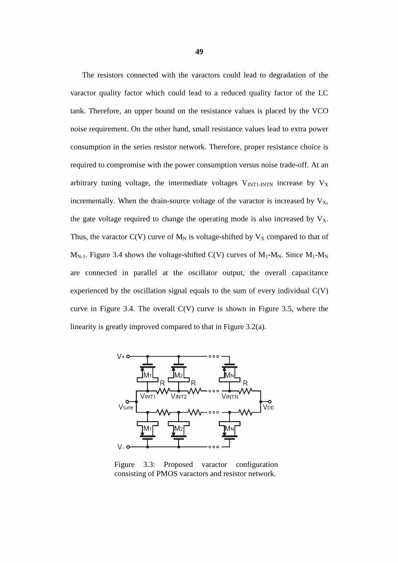
49
The resistors connected with the varactors could lead to degradation of the
varactor quality factor which could lead to a reduced quality factor of the LC
tank. Therefore, an upper bound on the resistance values is placed by the VCO
noise requirement. On the other hand, small resistance values lead to extra power
consumption in the series resistor network. Therefore, proper resistance choice is
required to compromise with the power consumption versus noise trade-off. At an
arbitrary tuning voltage, the intermediate voltages VINT1-INTN increase by VX
incrementally. When the drain-source voltage of the varactor is increased by VX,
the gate voltage required to change the operating mode is also increased by VX.
Thus, the varactor C(V) curve of MN is voltage-shifted by VX compared to that of
MN-1. Figure 3.4 shows the voltage-shifted C(V) curves of M1-MN. Since M1-MN
are connected in parallel at the oscillator output, the overall capacitance
experienced by the oscillation signal equals to the sum of every individual C(V)
curve in Figure 3.4. The overall C(V) curve is shown in Figure 3.5, where the
linearity is greatly improved compared to that in Figure 3.2(a).
Figure 3.3: Proposed varactor configuration consisting of PMOS varactors and resistor network.

50
To model the C(V) curve mathematically, the continuous varactor C(V)
curve is modeled by a piece-wise linear curve as shown in Figure 3.6, where the
continuous transition region from the inversion mode to the depletion mode is
modeled by a ramp with a ramp width of VW. Two constant sections with
capacitances Cmax and Cmin are used to model the sections where the
capacitance variation is small. Therefore, the slope of the ramp is given by,
Figure 3.4: C(V) curves of the varactors M1-MN.
Figure 3.5: Simulation of the overall C(V) curve at the oscillator output.

51
max min .rampW
C Ck
V
−= (3.4)
At an arbitrary tuning voltage, the gate voltage when the voltage difference
across the varactor equals to the threshold voltage is marked as V1+αVW, where α
is in percentage. The corresponding capacitance at V1+αVW is between Cmax and
Cmin. Therefore, the voltage V1, which marks the boundary between the Cmax
section and the ramp section, is given by,
1 .tune th WV V V Vα= − − (3.5)
Similarly, the operating mode of Mn starts to change at Vn, where Vn is given by,
( )1 .n tune th W XV V V V n Vα= − − + − (3.6)
At VY, the operating mode of M1-MN have all changed into the depletion mode,
and VY exceeds VN by VW as,
( ) ( )1 1 .Y tune th W XV V V V N Vα= − + − + − (3.7)
Figure 3.6: Approximate piece-wise linear C(V) curves.

52
By substituting Equation (3.3) into Equation (3.7), VY evaluates to,
( ) 11 .tune
Y th W DD
V NV V V V
N Nα −= − + − + (3.8)
Therefore, VY weakly depends on the tuning voltage when N is set to a large
value.
Any two adjacent C(V) curves are separated by VX. When VX exceeds VW, a
gate voltage interval VX −VW exists where the capacitance of every C(V) curve is
either Cmax or Cmin as shown in Figure 3.6. As a result, when the C(V) curves are
added, the overall C(V) curve consists of successive ramp sections and constant
sections instead of the linear profile shown in Figure 3.5. Therefore, VX is set to
match VW to ensure the linearity of the C(V) profile. When the C(V) curves of
M1-MN are added, the overall C(V) profile also consists of a ramp section and two
constant sections as shown in Figure 3.7. The capacitance of the two constant
sections equals to NCmax and NCmin. The slope of the ramp equals to,
Figure 3.7: Overall piece-wise linear C(V) curve.
53
( )
max min max min
1
.1
YW DD tune
NC NC NC NCk
NV V V V VN
− −= − = − −− + − (3.9)
The magnitude of the slope is minimum when the tuning voltage is 0V. As the
tuning voltage increases, V1 gradually approaches VY. When the tuning voltage is
VDD, the voltage difference between VY and V1 is reduced to VW. It can be
verified that when the tuning voltage is increased to VDD, Equation (3.9) evaluates
to,
max min ,W
NC NCk
V
−= − (3.10)
The effective capacitance experienced by the oscillation signal over the
oscillation period depends on the C(V) profile within the oscillation signal voltage
span. As shown in Figure 3.7, the oscillation signal amplitude is bounded by VCM
± VA over the oscillation period, where VCM is the common-mode voltage of the
oscillation signal. The capacitance traversed by the oscillation signal varies with
respect to the tuning voltage, where two different scenarios can be categorized. In
the first scenario, the C(V) profile is strictly linear within the oscillation
amplitude span as illustrated by the red sections in Figure 3.7. In the second
scenario, the oscillation signal traverses both the NCmax section and the linear
section as highlighted by the green regions. The boundary which separates the
two operating scenarios is when V1 equals to VCM −VA. Based on Equation (3.5),
the corresponding tuning voltage evaluates to,
54
.tune CM A th WV V V V Vα= − + + (3.11)
The effective capacitance is evaluated by a time-averaged approach. Though
not very accurate, it provides a good indication on how the effective capacitance
varies with respect to the tuning voltage. In the first scenario, since the C(V)
profile over the oscillation signal voltage span is linear, the time-averaged
capacitance equals to the instantaneous capacitance evaluated at VCM, which
evaluates to,
( )
( )1 max 1
1max max min
1
.
eff CM
CM
Y
C NC V V k
V VNC NC NC
V V
= + −
−= − −−
(3.12)
Also, since the oscillation frequency is given by Equation (3.13), the frequency
variation with respect to the tuning voltage can be evaluated as that in Equation
(3.14).
1
1,
effLCω = (3.13)
( )( )( )( )
1
1
max min3
1 max max min min 1
.2
tune tune
Y CM
Y Y CM
V
V V V
NC NC V V
L V V NC V NC NC V NC V
ω ω ∂∂ ∂=∂ ∂ ∂
− −= −
− − − −
(3.14)
Since, VY weakly depends on the tuning voltage, the numerator can be treated
as a constant. The denominator consists of a quadratic function with V1 as the
variable. Since V1 linearly depends on the tuning voltage as given by Equation
(3.5), Equation (3.14) can be represented as,

55
( )2 .
tune tune
a
V b V
ω∂ ∝ −∂ −
(3.15)
By integrating Equation (3.15) with respect to Vtune, the oscillation frequency
varies with respect to the tuning voltage as,
.tune
a
b Vω ∝
− (3.16)
In the second scenario, the oscillation signal traverses two different sections of
the C(V) profile. In particular, the percentage time the oscillation signal stays in
the NCmax section is V1 − (VCM −VA) out of 2VA, and the percentage time in the
linear section is VCM+VA −V1 out of 2VA as indicated in Figure 3.7. Therefore,
the effective capacitance is given by,
( ) ( ) ( )
( ) ( )( )
1 1 12 max max
2
max min 1max
1
2 2 2
.4
CM A CM A CM Aeff
A A
CM A
A Y
V V V V V V V V VC NC NC k
V V
NC NC V V VNC
V V V
− − + − + − = + +
− + −= −
−
(3.17)
By substituting Equation (3.17) into Equation (3.13),
( ) ( )( )
( )
2
max 1 max min 1
1
1.
4
4A Y CM A
A Y
LNC V V V L NC NC V V V
V V V
ω =− − − + −
−
(3.18)
Since, the denominator consists of a second order polynomial divided by a first
order polynomial, the oscillation frequency can be approximated as,
1
.tunea V
ω ∝−
(3.19)

56
3.2 Experimental Results and Discussion
A single-switch (SS) LC-VCO is implemented with TSMC 0.18µm CMOS
technology as shown in Figure 3.8. The die microphotograph is shown in Figure
3.9, and the chip area is 1.25mm2. The proposed varactor configuration as shown
in Figure 3.3 is implemented with 15 PMOS varactors and 15 resistors. The
dimension of each varactor is 150µm by 0.18µm and the value of the resistance R,
is 200Ω. The square integrated inductor is implemented with the top metal layer,
where the metal sheet resistance is 0.036Ω/. The simulated inductance is 4.8nH
with a quality factor of 5.1 at 1GHz. The VCO draws 4mA of current from a 1.8V
power supply. The measured and simulated frequency tuning curves are shown in
Figure 3.10, where the frequency tuning ranges are 9.5% and 8.2%, respectively.
The VCO gains of the measured and simulated tuning curves are 37MHz/V and
60MHz/V, respectively. The phase noise measurement is shown in Figure 3.11,
Figure 3.8: Schematic of the fabricated single-switch (SS) LC-VCO. Transistor sizes: W1 = 360µm, L1 = 2.7µm, W2-3 = 120µm, L2-3 = 0.3µm.
57
where the phase noise is measured to be -117dBc/Hz at 1MHz frequency offset,
and -125dBc/Hz at 3MHz frequency offset. The simulated signal amplitude at
1GHz and the first five harmonics are shown in Figure 3.12. The measured output
signal spectrum at 1GHz is shown in Figure 3.12. The VCO performances
between similar designs are summarized in Table 3.1.
Figure 3.9: Die microphotograph of the designed SS LC-VCO.
Figure 3.10: Top: Measured SS LC-VCO frequency tuning curve. Bottom: Simulated SS LC-VCO frequency tuning curve.

58
As mentioned previously, the effective capacitance experienced by the
oscillation signal over the oscillation period can be categorized into two scenarios.
As a result, the oscillating frequency and the tuning voltage dependency vary
between the two scenarios. The tuning voltage which separates the two scenarios
is given by Equation (3.11). If VCM equals to VDD, VA is roughly 0.9V, Vth is
taken as 0.4V, and αVW is estimated to be 0.1V, then the tuning voltage is
Figure 3.12: Simulated signal amplitude of the fundamental tone at 1GHz and the first five harmonics.
Figure 3.11: Measurement results of SS LC-VCO phase noise.

59
calculated to be 1.4V. For the simulated frequency tuning curve in Figure 3.10,
the frequency and tuning voltage dependency are separated into two different
regions when the tuning voltage reaches 1.2V. When the tuning voltage is less
than 1.2V, the tuning curve is linear and the dependency is modeled by Equation
(3.16). As the tuning voltage continues to increase, the dependency is modeled by
Equation (3.19). Similar results can also be observed in the measured frequency
tuning curve.
3.3 Conclusions
A technique to improve the linearity of the oscillation frequency tuning curve
for LC-VCO with an inversion-mode varactor is described in this Chapter. The
proposed technique improves the frequency tuning curve through linearization of
the varactor C(V) characteristics. The designed varactor configuration consists of
multiple varactor units, which are connected to the oscillator output at one end,
Figure 3.13: Measured VCO output spectrum.
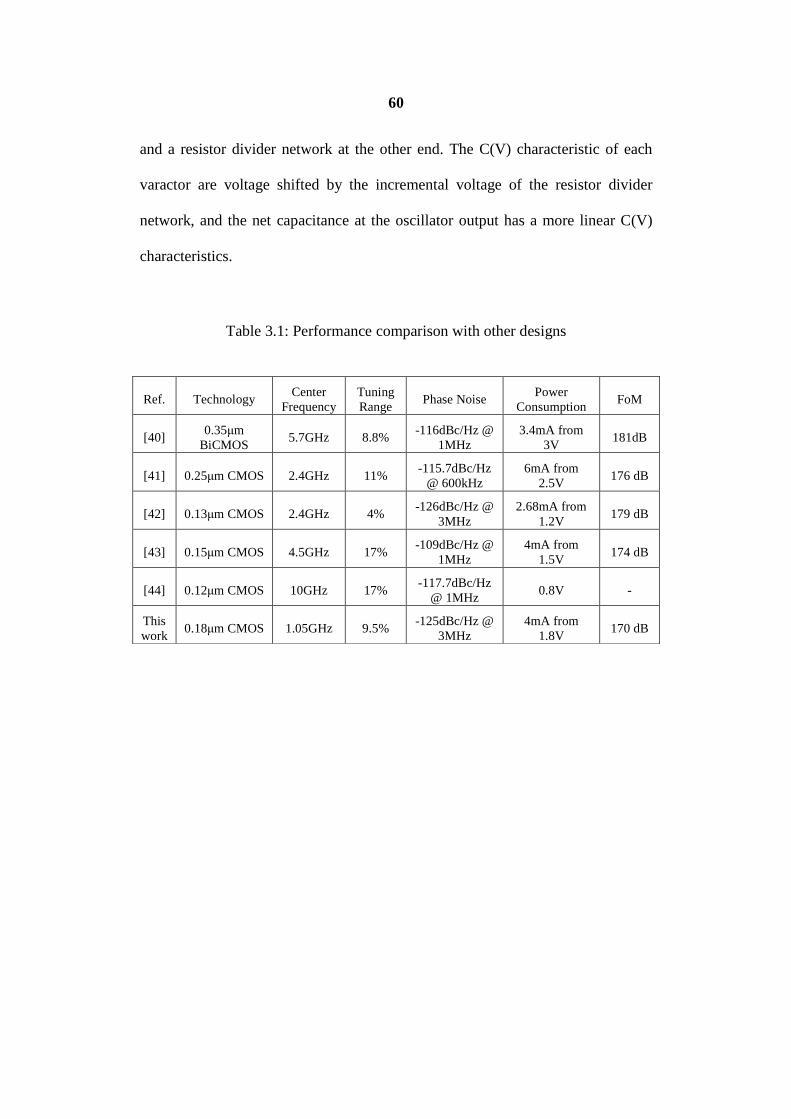
60
and a resistor divider network at the other end. The C(V) characteristic of each
varactor are voltage shifted by the incremental voltage of the resistor divider
network, and the net capacitance at the oscillator output has a more linear C(V)
characteristics.
Table 3.1: Performance comparison with other designs
Ref. Technology Center
Frequency Tuning Range
Phase Noise Power
Consumption FoM
[40] 0.35µm
BiCMOS 5.7GHz 8.8%
-116dBc/Hz @ 1MHz
3.4mA from 3V
181dB
[41] 0.25µm CMOS 2.4GHz 11% -115.7dBc/Hz
@ 600kHz 6mA from
2.5V 176 dB
[42] 0.13µm CMOS 2.4GHz 4% -126dBc/Hz @
3MHz 2.68mA from
1.2V 179 dB
[43] 0.15µm CMOS 4.5GHz 17% -109dBc/Hz @
1MHz 4mA from
1.5V 174 dB
[44] 0.12µm CMOS 10GHz 17% -117.7dBc/Hz
@ 1MHz 0.8V -
This work
0.18µm CMOS 1.05GHz 9.5% -125dBc/Hz @
3MHz 4mA from
1.8V 170 dB

61
CHAPTER 4: TIME-WEIGHTED OSCILLATING
FREQEUCNY MODEL FOR LC-VCO WITH
IMPROVED PHASE NOISE PERFORMANCE
In this Chapter, the oscillating frequency tuning model and the phase noise
improvement issues of LC-VCO are examined more closely. As previously
mentioned, integrated LC-VCOs as shown in Figure 4.1(a) are widely used in
modern wireless transceivers due to their superior phase noise performance as
opposed to their counterparts such as the ring oscillators. Noises associated with
the active and passive components are converted into the phase noise through
different mechanisms, which are well summarized by Rael and Abidi [45]. In
particular, two different sources have profound contributions to the phase noise
performance. The first source is the flicker noise associated with the tail biasing
transistor. This low-frequency noise enters the resonator as the amplitude-
modulated (AM) noise, which is then converted into the phase-modulated (PM)
noise through the varactor. The second source is the thermal noise of the tail
biasing transistor at twice of the oscillation frequency 2ω, which is down-
converted to the close-in phase noise of the carrier through the interaction with
the carrier. Different techniques have been proposed to reduce the incurred phase
noise due to both sources. To reduce the impact of the low-frequency flicker
noise, one method is to reduce the varactor sensitivity with respect to the AM
noise through a new varactor configuration as described by Bonfanti et al. [46].
To reduce the thermal noise of the tail transistor at 2ω, the filter technique in

62
Hegazi et al. [17] is proposed, where high impedance with a resonant frequency
of 2ω is added between the tail transistor and the LC tank.
The novelty of the current work is twofold. First, a low-power LC-VCO is
designed where the impact of both sources of phase noise are reduced
simultaneously. Instead of adding the high impedance at 2ω as proposed in [17], a
2nd order RLC notch filter is connected between the tail biasing transistor and the
LC tank to suppress the noise power at 2ω as shown in Figure 4.1(b). To reduce
the impact of the tail transistor flicker noise up-conversion, passive capacitors are
added with the varactor in parallel as designed in [47]. In this paper, a new
varactor configuration with the addition of a capacitor divider network is designed
to decrease the strength of the AM-to-PM noise conversion as shown in Figure
Figure 4.1: (a) The schematic of a typical top-biased integrated LC-VCO. (b) The schematic of the integrated VCO with the proposed 2nd order notch filter, and the proposed varactor structure with the capacitor divider network.

63
1(b). Capacitor C2 provides an extra path to partially filter the AM noise entering
the varactor. Further, we develop a new model for the LC-VCO oscillation
frequency based on a new time-weighed approach. Since, it is difficult to make
the on-chip spiral inductor tunable, the variation in the oscillation frequency
comes from the tunable capacitance of the varactor. The instantaneous
capacitance experienced by the oscillating signal varies from one time instance to
another; hence, the effective capacitance experienced by the oscillating signal
over an oscillation period cannot be accurately represented by the C(V)
characteristics of the varactor. Instead, the effective capacitance needs to
represent the contribution of the instantaneous capacitance at each time instance
within the oscillation period. Therefore, the challenge faced in modeling the
oscillation frequency is to model the effective capacitance, which depends on the
tuning voltage, the oscillating amplitude, and the C(V) characteristics of the
varactor. The effective capacitance is modeled in several previous studies such as
in references [36][48][49]. Though accurate, these models have not accounted for
the gate-source and gate-drain capacitance associated with the switching
transistors. Also, the C(V) profile is approximated by a step function, and a more
accurate model for the C(V) profile could lead to more accurate prediction of the
oscillation frequency. Therefore, in this work, a new model for the oscillation
frequency based on a time-weighted approach is proposed. The C(V) curve is
modeled by a piece-wise linear profile consisting of three linear sections. The
modeled effective capacitance accounts for both the varactor capacitance, and the
oxide capacitance of the switching transistors. Based on the developed model, it is
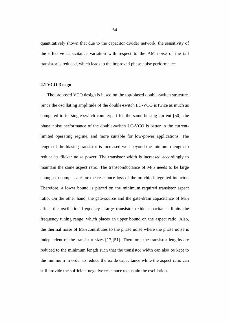
64
quantitatively shown that due to the capacitor divider network, the sensitivity of
the effective capacitance variation with respect to the AM noise of the tail
transistor is reduced, which leads to the improved phase noise performance.
4.1 VCO Design
The proposed VCO design is based on the top-biased double-switch structure.
Since the oscillating amplitude of the double-switch LC-VCO is twice as much as
compared to its single-switch counterpart for the same biasing current [50], the
phase noise performance of the double-switch LC-VCO is better in the current-
limited operating regime, and more suitable for low-power applications. The
length of the biasing transistor is increased well beyond the minimum length to
reduce its flicker noise power. The transistor width is increased accordingly to
maintain the same aspect ratio. The transconductance of M2-5 needs to be large
enough to compensate for the resistance loss of the on-chip integrated inductor.
Therefore, a lower bound is placed on the minimum required transistor aspect
ratio. On the other hand, the gate-source and the gate-drain capacitance of M2-5
affect the oscillation frequency. Large transistor oxide capacitance limits the
frequency tuning range, which places an upper bound on the aspect ratio. Also,
the thermal noise of M2-5 contributes to the phase noise where the phase noise is
independent of the transistor sizes [17][51]. Therefore, the transistor lengths are
reduced to the minimum length such that the transistor width can also be kept to
the minimum in order to reduce the oxide capacitance while the aspect ratio can
still provide the sufficient negative resistance to sustain the oscillation.

65
The relative transistor size ratio between M2-3 and M4-5 also affects the
common-mode voltage of the oscillating signal. In the current-limited operating
regime, the oscillating amplitude increases linearly with respect to the biasing
current. The oscillating amplitude is bounded by the analog ground at the peak,
and the ground rail at the trough. As the oscillating amplitude gradually
approaches the two boundaries, it starts to saturate and becomes independent of
the biasing current, and the oscillator enters the voltage-limited operating regime.
Therefore, the oscillating amplitude should be biased at the boundary between the
current-limited and the voltage-limited operating regime for optimal phase noise
performance [52] and the phase noise performance improves as the signal power
increases [53]. Intuitively, the common-mode voltage of the oscillating signal
should be placed at the middle between the analog ground and the ground rail
such that the equal amplitude spans are maximized in both directions. This can be
easily achieved by matching the transconductance of M2-3 to M4-5. This requires
that W2-3 should be two or three times larger than W4-5 in order to compensate for
the body effect experienced by M2-3, and the majority carrier mobility difference
between the PMOS and NMOS devices. Note that the matching of the
transconductance is based on hand analysis while PVT changes can lead to
unpredictable common-mode voltage variation.
The variation in the oscillating frequency depends on the tunable capacitance
of the varactor. The proposed varactor structure in Figure 4.1(b) consists of
66
passive capacitors and inversion-mode PMOS varactor. A capacitor divider
network consisting of C1-3 is added to reduce the flicker noise up-conversion
effect due to the presence of the varactor. Therefore, the instantaneous effective
capacitance in parallel with the inductor is,
( ) ( )1 2 var 3 2 4 2 4|| 4 .eff gd gd gs gsC C C C C C C C C= + + + + + + (4.1)
Also, digital switches controlled by VC1-2 are added to extend the frequency
tuning range.
4.2 Frequency Estimation based on the Time-Weighted Approach
An accurate snapshot of the instantaneous oscillating frequency of the LC-
tank based oscillator is given by,
2
11 ,S eff
eff
R C
LLCω = − (4.2)
where, RS is the series resistance associated with the tank inductor. On one hand,
Equation (4.2) can accurately model the oscillation frequency of the LC oscillator
with the passive capacitor since the effective capacitance remains constant over
the oscillating cycle and thus the instantaneous oscillation frequency is invariant
with respect to time. On the other hand, to predict the oscillation frequency of a
varactor-based oscillator with Equation (4.2), the effective capacitance which
accounts for the capacitance variation over the entire oscillating cycle must be
modeled and used in the calculation such that the varactor-based oscillator can be
treated as an inductor oscillating with a passive capacitor with the modeled
effective capacitance.

67
In references [48] and [49], the closed-form expressions of the effective
capacitance are provided by balancing the inductor and the capacitor current
where the harmonics are accounted. Since the proposed expressions of the
effective capacitance has not modeled the oxide capacitance associated with the
switching transistors, a new approach is proposed in this work to model the
effective capacitance experienced by the oscillating signal over an oscillation
period, where both the varactor capacitance, and the gate-source and gate-drain
capacitances of the switching transistors are accounted. We will later show that
the calculated oscillation frequency based on the modeled effective capacitance is
in good agreement with the simulation results.
The inversion-mode PMOS varactor capacitance variations with respect to the
gate voltage variations at five different tuning voltages are shown in Figure 4.2.
Figure 4.2 Simulated C(V) characteristics of the PMOS varactor at five different tuning voltages.

68
Over a single oscillating period, the oscillating signal amplitude spans over a
different portion of the C(V) curve, which translates into the variation of the
oscillation frequency. For example, when the tuning voltage is at 1.8V, the
oscillating signal sweeps the portion of the C(V) curve with the maximum
capacitance values, which leads to the lowest oscillation frequency. On the other
hand, the oscillating signal sweeps the portion of the C(V) curve with the
minimum capacitance values, which leads to the highest oscillation frequency
when the tuning voltage is at 0V.
At different tuning voltages, the ease to estimate the effective capacitance
over an oscillating period depends on the linearity of the C(V) profile at that
tuning voltage. On one hand, at the tuning voltages of 0V and 1.8V, the effective
capacitance can be modeled by averaging the varactor capacitance values over the
voltage span of the oscillating signal, and the instantaneous oscillation frequency
at any time instant within the oscillating period is the same. On the other hand, a
much more nonlinear C(V) profile is experienced by the oscillating signal when
the tuning voltage is at 0.9V. Since the varactor capacitance at every time instance
differs from one another, the instantaneous oscillation frequency varies from time
to time. To model the effective capacitance for the nonlinear C(V) profile,
averaging the varactor capacitance over the voltage span of the oscillating signal
leads to inaccurate results due to the sinusoidal nature of the oscillating signal
waveform. As shown in Figure 4.3, for the same incremental change in the
voltage ∆V1 and ∆V2, the associated time intervals ∆T1 and ∆T2 differ from each

69
other. Due to the differences in the time intervals, the varactor capacitance
accumulated within the same voltage increment ∆V varies since the oscillating
signal sweeps different portions of the C(V) curve at different paces. For example,
the oscillating signal spends more time in section ∆V1 of the C(V) curve than in
section ∆V2. Therefore, the accumulated capacitance within ∆V1 will be larger
than that in ∆V2 since both the capacitance values and the corresponding time
intervals are greater. This capacitance-time dependency has been taken into
account in modeling the effective capacitance, where the contribution of each
varactor capacitance segment to the effective capacitance over an oscillating cycle
has been weighted based on the time duration the oscillating signal spent within
that segment.
Figure 4.3: The capacitance-time dependency effect experienced by the oscillating signal.

70
The accuracy of the time-weighted approach is first verified with experimental
data. At each tuning voltage, the varactor capacitance over the oscillating signal
amplitude as highlighted by the black portions of the C(V) curve in Figure 4.2 is
simulated. Then, the C(V) curve is evenly divided into N sections as shown in
Figure 4.3, where there is a one-to-one mapping between the capacitance CN and
the oscillating signal voltage VN. Each VN corresponds to a time instance, TN. The
percentage of the time interval ∆TN weighted within the oscillating period is
calculated by,
1 1
1cos cos% .
2N N
N
V VT
π
− −+ −∆ = (4.3)
The percentage matrix ∆TN% is then multiplied by the capacitance matrix C1-N to
ensure that the contribution of the different portions of the C(V) curve is weighted
based on the magnitude of the time intervals ∆TN. Then, all the entries of the
product matrix are added, and the sum represents the effective varactor
capacitance over an oscillating cycle.
The effective gate-source and gate-drain capacitances over an oscillating cycle
have been modeled in a similar way. The oscillating amplitude of the typical LC-
VCO can drive the switching transistors into the deep triode region for almost half
of the oscillating cycle, and the cut-off state for the other half with a small time
period in the saturation region in between as shown in Figure 4.4. The gate-source
and gate-drain capacitances of the MOS transistors are modeled by Equations
(4.4) and (4.5). In the saturation region,

71
2
30,
gs OX
gd
C C WL
C
=
= (4.4)
and in the triode region,
1
.2gs gd OXC C C WL= = (4.5)
The time interval, Tsat, where both the PMOS and the NMOS transistors are in the
saturation region is approximated based on T2, where T2 is the time instance when
the differential signal voltage equals to the transistor threshold voltage as,
( )22 cos ,A THV T Vω− = (4.6)
and Tsat is given by,
12
22 cos ,
4 2 2TH
satA
VT TT T
Vω− = − = − −
(4.7)
where, T is the oscillating signal period. As a result, the percentage of the time
interval with respect to the oscillating period where both the transistors are in the
saturation region is 2Tsat divided by T. The effective gate-source capacitance over
an oscillating cycle is then given by,
Figure 4.4: The different operating regions experienced by the switching transistors over an oscillating cycle.

72
2 22 1
,3 2 2
sat satox ox
T T TC WL C WL
T T
− +
(4.8)
and the effective gate-drain capacitance over an oscillating cycle is given by,
2 1
.2 2
satox
T TC WL
T
−
(4.9)
The varactor capacitance, gate-source, and gate-drain capacitances of the
switching transistors are substituted into Equation (4.1) to calculate the effective
capacitance, which is then substituted into Equation (4.2) to calculate the
oscillation frequency.
The comparison of the frequency tuning curve between the calculated
frequency and simulated frequency is shown in Figure 4.5, where the calculated
frequency tuning curve has preserved the geometric characteristic of the simulated
curve with numerical differences. The error in percentage is also shown in Figure
4.5, where the error is less than 1% in general. As a result, the time-weighted
approach is an effective method to model the oscillating frequency of a general
LC-VCO. The described process of modeling the oscillating frequency heavily
depends on the characteristics of the varactor C(V) profile, where the varactor
capacitance over the oscillating signal voltage span at every tuning voltage of
interest must be simulated in order to predict the oscillating frequency. To reduce
the effort required to model the frequency tuning curve, the non-linear varactor
C(V) profile is modeled by a piece-wise linear C(V) profile as shown in Figure
4.6. The linear profile consists of two constant sections with capacitance values of
Cmax and Cmin, and a ramp section with the ramp width VW. The values of VW,
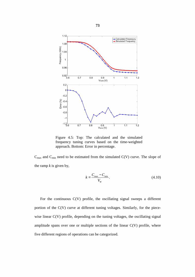
73
Cmax and Cmin need to be estimated from the simulated C(V) curve. The slope of
the ramp k is given by,
max min .W
C Ck
V
−= (4.10)
For the continuous C(V) profile, the oscillating signal sweeps a different
portion of the C(V) curve at different tuning voltages. Similarly, for the piece-
wise linear C(V) profile, depending on the tuning voltages, the oscillating signal
amplitude spans over one or multiple sections of the linear C(V) profile, where
five different regions of operations can be categorized.
Figure 4.5: Top: The calculated and the simulated frequency tuning curves based on the time-weighted approach. Bottom: Error in percentage.

74
In the first region, the oscillating signal amplitude only sweeps the Cmin
section of the C(V) curve as illustrated in Figure 4.7. When the tuning voltage is
at 0V, the oscillating signal is far from the ramp section. As the tuning voltage
increases, the oscillating signal gradually approaches the ramp section until it
reaches the boundary between the Cmin and the ramp section at a certain tuning
voltage V1 as shown in Figure 4.7. V1 is determined based on the assumption that
the varactor capacitance equals to CX (where CX is between Cmax and Cmin) when
the voltage difference across the varactor equals to the transistor threshold
voltage. This is a reasonable assumption since the threshold voltage marks the
boundary of the transistor operating modes between the inversion mode and the
depletion mode [39]. At CX, the corresponding gate voltage is within VW, and its
location is indicated by αVW. The unit of α is percentage, and its value also needs
to be estimated from the simulated C(V) curve. When the gate voltage of the
Figure 4.6: The piece-wise linear C(V) profile used to model the continuous C(V) curve.
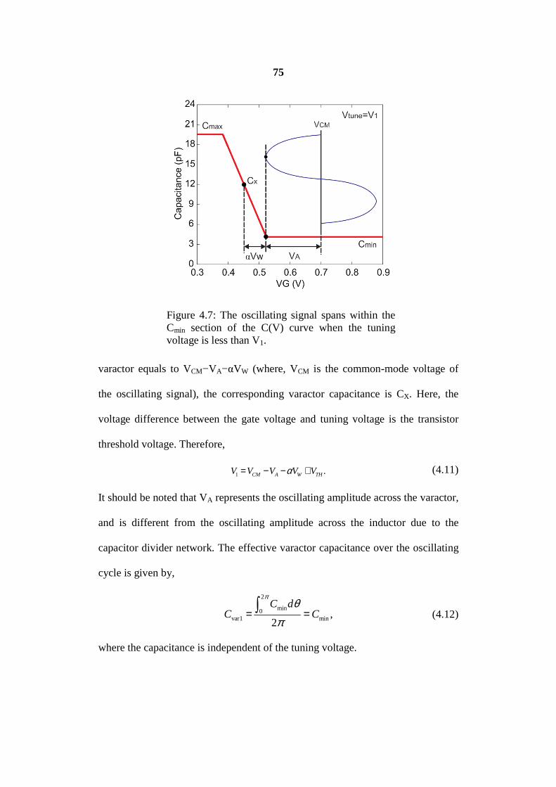
75
varactor equals to VCM−VA−αVW (where, VCM is the common-mode voltage of
the oscillating signal), the corresponding varactor capacitance is CX. Here, the
voltage difference between the gate voltage and tuning voltage is the transistor
threshold voltage. Therefore,
1 .CM A W THV V V V Vα= − − + (4.11)
It should be noted that VA represents the oscillating amplitude across the varactor,
and is different from the oscillating amplitude across the inductor due to the
capacitor divider network. The effective varactor capacitance over the oscillating
cycle is given by,
2
min0var1 min,2
C dC C
πθ
π= =∫
(4.12)
where the capacitance is independent of the tuning voltage.
Figure 4.7: The oscillating signal spans within the Cmin section of the C(V) curve when the tuning voltage is less than V1.
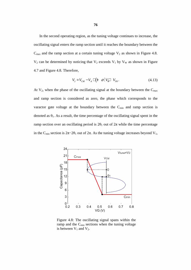
76
In the second operating region, as the tuning voltage continues to increase, the
oscillating signal enters the ramp section until it reaches the boundary between the
Cmax and the ramp section at a certain tuning voltage V2 as shown in Figure 4.8.
V2 can be determined by noticing that V2 exceeds V1 by VW as shown in Figure
4.7 and Figure 4.8. Therefore,
( )2 1 .CM A W THV V V V Vα= − + − + (4.13)
At V2, when the phase of the oscillating signal at the boundary between the Cmax
and ramp section is considered as zero, the phase which corresponds to the
varactor gate voltage at the boundary between the Cmin and ramp section is
denoted as θ1. As a result, the time percentage of the oscillating signal spent in the
ramp section over an oscillating period is 2θ1 out of 2π while the time percentage
in the Cmin section is 2π−2θ1 out of 2π. As the tuning voltage increases beyond V1,
Figure 4.8: The oscillating signal spans within the ramp and the Cmin sections when the tuning voltage is between V1 and V2.

77
the oscillating signal enters the ramp section, and θ1 gradually moves away from
zero phase. The magnitude of the extra tuning voltage above V1 is related to θ1 by,
( )1 1cos .A A tuneV V V Vθ = − − (4.14)
Therefore,
( )11
1 cos .A tune
A
V V V
Vθ − − −
= (4.15)
When the tuning voltage is V1, θ1 evaluates to zero which indicates that θ1
coincides with the zero phase. At an arbitrary tuning voltage between V1 and V2,
the instantaneous capacitance experienced by the oscillating signal at an arbitrary
phase θ between phase zero and θ1 is determined by considering the magnitude of
the phase difference between θ and θ1 as,
( )min 1C cos cos .AkV θ θ+ − (4.16)
It can be verified that when θ is zero and the tuning voltages are V1 and V2,
Equation (4.16) evaluates to Cmin and Cmax respectively as expected. The effective
varactor capacitance over an oscillating cycle is evaluated by integrating (4.16)
over the appropriate phase intervals as,
( )1 1
1
2
min min 102 cos cos
,2
AC d C kV dπ θ θ
θθ θ θ θ
π
−+ + −∫ ∫
(4.17)
where, the two integrals represent the effective varactor capacitance accumulated
within Cmin and the ramp section, respectively. The above expression evaluates to,
( )var2 min 1 1 1sin cos .AkVC C θ θ θ
π= + − (4.18)

78
When the tuning voltage equals to V1, Equation (4.18) evaluates to Cmin as
expected.
In the third operating region, the oscillating signal spans within all three
sections of the C(V) curve as illustrated in Figure 4.9(a). The time percentages of
the oscillating signal spent in the Cmin and the Cmax sections are 2π−2θ1 and 2θ2
out of 2π, respectively. The time percentage in the ramp section is 2(θ1−θ2) out of
2π. θ2 is determined similarly as θ1 by considering the magnitude of the extra
tuning voltage above V2 as,
( )21
2 cos .A tune
A
V V V
Vθ − − −
= (4.19)
When the tuning voltage is V2, θ2 evaluates to zero which indicates that θ2
coincides with zero phase as illustrated in Figure 4.8. When the tuning voltage is
V3, the oscillating signal reaches the boundary between the Cmax and the ramp
section as shown in Figure 4.9(b), where θ1 evaluates to π. V3 is determined in
Figure 4.9: The oscillating signal spans within all three sections when (a) the tuning voltage is between V2 and V3 and (b) the tuning voltage is V3.
79
similar way as V1 and V2 by noticing that the varactor gate voltage is VCM
+VA−αVW when the corresponding capacitance is CX. Therefore,
3 .CM A W THV V V V Vα= + − + (4.20)
Another way to determine V3 is by noticing that V3 exceeds V1 by 2VA as shown
in Figure 4.7 and Figure 4.9(b). The effective varactor capacitance is determined
by integrating the instantaneous capacitance over the oscillating period as,
( )2 1 1
1 2
2
max min min 102 2 cos cos
,2
AC d C d C kV dθ π θ θ
θ θθ θ θ θ θ
π
−+ + + −∫ ∫ ∫
(4.21)
where, the three integrals represent the varactor capacitance in the Cmax, Cmin, and
the ramp section. The above expression evaluates to,
( ) ( ) ( )max min 2
var3 min 1 2 1 2 1sin sin cos .A AC C kV kV
C Cθ
θ θ θ θ θπ π π
−= + + − − − (4.22)
In the fourth operating region, the oscillating signal gradually pulls away from
the ramp section until it reaches the boundary between the Cmax and the ramp
section at the tuning voltage V4 as shown in Figure 4.10. By comparing Figure
4.9(b) and Figure 4.10, it is noticed that V4 exceeds V3 by VW thus,
( )4 1 ,CM A W THV V V V Vα= + + − + (4.23)
where, θ2 evaluates to π at V4. The oscillating signal spends 2π−2θ2 out of 2π
percent of the time in the ramp section, and 2θ2 out of 2π percent of the time in the
Cmax section. The effective capacitance is determined by,
( )2 2
2
2
max max 202 cos cos
.2
AC d C kV dθ π θ
θθ θ θ θ
π
−+ − −∫ ∫
(4.24)

80
The expression evaluates to,
( )var 4 max 2 2 2 2cos sin cos .AkVC C θ θ θ π θ
π= − − − (4.25)
At V4, the effective varactor capacitance evaluates to Cmax.
In the last operating region, the oscillating signal spans within the Cmax section
only, and the effective varactor capacitance evaluates to,
2
max0var5 max.2
C dC C
πθ
π= =∫
(4.26)
The values of V1-4 are calculated with an iterative approach due to the
presence of the varactor body effect and the oscillating signal amplitude variation
with respect to the oscillating frequency. Since the source and drain voltages of
the PMOS varactor are tied together, the transistor threshold voltage varies with
Figure 4.10: The oscillating signal spans within the Cmax section when the tuning voltage exceeds V4.
81
respect to the tuning voltage. This non-ideality is modeled by the well-known
second-order body effect expression,
( )( )0 2 2 .TH TH F tune DD FV V V Vγ= + Φ + − − Φ (4.27)
Also, the oscillating amplitude VA depends on the oscillation frequency, which
depends on the tuning voltage. A linear approximation of the amplitude variation
is used in the calculation, where the exact maximum and minimum oscillating
amplitudes (Vmax and Vmin) are obtained from the simulation results at the two
extremes of the tuning voltages. At an arbitrary tuning voltage, VA is given by,
max minmax .A tune
DD
V VV V V
V
−= −
(4.28)
When the tuning voltage equals to zero and VDD, VA evaluates to Vmax and Vmin,
respectively. Therefore, to calculate V1, it needs to satisfy Equations (4.11)
(4.27)(4.28) simultaneously. This is achieved through an iterative approach where
an initial guess of the tuning voltage is used in the calculation. Based on the
differences in the calculated threshold voltage between Equations (4.11) and
(4.27), the tuning voltage is adjusted accordingly until the difference between the
calculated threshold voltages is negligible.
The effective varactor capacitance Cvar1 to Cvar5 is calculated and substituted
into Equation (4.1) to calculate the effective capacitance. Then, the oscillation
frequency is calculated with Equation (4.2). The comparison between the
calculated and the simulated frequency tuning curve is shown in Figure 4.11. The
errors in percentage are also shown in Figure 4.11, where the maximum error is at

82
2%. The main source of the discrepancy is the inaccuracy in modeling the
continuous C(V) curve with the piece-wise linear C(V) curve. For example,
between V1 and V2, the varactor capacitance is over-estimated, which leads to
lower calculated oscillating frequency compared with the simulated frequency.
Also, between V3 and V4, the varactor capacitance is under-estimated, which
leads to higher calculated oscillation frequency compared with the simulated
frequency.
Figure 4.11: Top: The calculated and the simulated frequency tuning curves based on the piece-wise linear C(V) curve and the time-weighted approach. Bottom: Error in percentage.

83
4.3 Phase Noise Reduction through the Capacitor Divider Network
The low-frequency flicker noise of the tail biasing current is up-converted into
the AM noise by the hard-switching action of the oscillating signal as in a mixer
[45][54]. The AM noise is then converted into PM noise through the varactor. The
phase noise due to the AM-to-PM conversion mechanism is quantified in
reference [46] as,
( ) ( )2
2.
2AM FM AM m
m
K S ωω
ω−=L (4.29)
SAM is the power spectral density of the amplitude noise, and is given in reference
[8] as,
( ) ( )2
,AAM m I
VS S
Iω ω∂ = ∂
(4.30)
where, SI is the power spectral density of the low-frequency flicker noise. For a
standard VCO as shown in Figure 4.1(a), the varactor directly connects to the
oscillator output. The oscillating amplitude is proportional to the biasing current
derived in reference [8] as,
2
,A PV IRπ
= (4.31)
and
2 2
2,A
P
VR
I π∂ = ∂
(4.32)
where, RP is the equivalent parallel resistance associated with the inductor. With
the addition of the capacitor divider network, the varactor is decoupled from the

84
oscillator output, where the oscillating amplitude at the varactor gate is reduced
to,
3
1 2 3 var
2,A P
CV IR
C C C Cπ
= + + + (4.33)
thus,
22 2
3
1 2 3 var
2.A
P
CVR
I C C C Cπ ∂ = ∂ + + +
(4.34)
Therefore, compared to Equation (4.32), the oscillator amplitude variation due to
the changes in the biasing current is greatly reduced, which leads to the reduced
flicker noise power entering the varactor and up-converting into phase noise.
KAM-FM is the sensitivity measurement of the oscillating frequency variation
with respect to the oscillating amplitude variation, and is expressed in reference
[8] as,
.AM FMA
KV
ω−
∂=∂
(4.35)
This derivative is evaluated by multiplying three partial derivatives as,
var
var
.effAM FM
eff A
C CK
C C V
ω−
∂ ∂∂=∂ ∂ ∂
(4.36)
The first partial derivative is evaluated by differentiating Equation (4.2) with
respect to Ceff, which evaluates to,
2 2
1.
2eff eff eff S effC C LC R C
ω∂ = −∂ −
(4.37)
85
The second partial derivative measures the sensitivity of the effective capacitance
variation with respect to the varactor capacitance variation. It is evaluated by
differentiating Equation (4.1) with respect to Cvar, which evaluates to,
( )
23
2var 1 2 3 var
.effC C
C C C C C
∂=
∂ + + + (4.38)
On the other hand, the instantaneous effective capacitance of the VCO in Figure
4.1 (a) is given by,
( )var 2 4 2 44 ,eff gd gd gs gsC C C C C C= + + + + (4.39)
and the second partial derivative evaluates to,
var
1.effC
C
∂=
∂ (4.40)
By comparing Equation (4.38) to (4.40), it is evident that the sensitivity of the
effective capacitance variation with respect to the varactor capacitance variation is
greatly reduced with the addition of the capacitor divider network, and this leads
to reduced KAM-FM magnitude and reduced AM noise up-converted into PM noise.
The third partial derivative measures the sensitivity of the varactor capacitance
variation with respect to the oscillating signal amplitude variation. It is evaluated
by differentiating Cvar1 to Cvar5 with respect to VA. For the first and the fifth
operating regions,
var1 var5 0.A A
C C
V V
∂ ∂= =∂ ∂
(4.41)
For the second and the fourth operating regions,
( )22
var2 ,A CM TH tune W
A A
k V V V V VC
V V
απ
+ − −∂ −=
∂ (4.42)

86
and
( )( )22
var41
.A CM TH tune W
A A
k V V V V VC
V V
απ
+ − + −∂ = −∂
− (4.43)
When the tuning voltage equals to V1 and V4, both Equations (4.42) and (4.43)
evaluate to zero, as expected. For the third operating region,
( ) ( )( )222 2
var3
1.
A CM TH tune W A CM TH tune W
A A
k V V V V V V V V V VC
V V
α α
π
− + − − − + − + − ∂ =∂
−
(4.44)
At a particular tuning voltage Vnull, Equation (4.44) evaluates to zero where,
( )2 3 0.5 .2null CM TH W
V VV V V Vα+= = + + − (4.45)
The varactor capacitance variation with respect to the oscillating signal
amplitude variation is shown in Figure 4.12. The varactor capacitance is immune
to the amplitude variation in operating region one and five, since the oscillating
signal experiences identical capacitance over the oscillation cycle. In operating
regions two to four, one portion of the oscillating signal is within the ramp section
of the C(V) curve. The variation in the oscillating amplitude affects the voltage
magnitude at every time instance within the oscillation period. The changes in the
voltage magnitude are converted into the capacitance variation through k in
Equation (4.10). When the tuning voltage is between V1 and VX, and between VY
and V4, VCM does not enter the ramp section, and only one side of the oscillating
signal enters the ramp section with VCM as the center. Therefore, the capacitance
variation is monotonic as the increase of the oscillating amplitude strictly leads to

87
the increase of the varactor capacitance, and vice versa. When the tuning voltage
is between VX and VY, VCM enters the ramp section, and both sides of the
oscillating signal stays within the ramp section. Therefore, the capacitance
variation is no longer monotonic, where the oscillating amplitude variation leads
to the increase of the capacitance on one side of VCM, and decreases on the other
side. Therefore, the net change in the capacitance is reduced for the same change
in the oscillating amplitude and thus the magnitude of the sensitivity starts to
decrease. At Vnull, the capacitance increase on one side of VCM cancels the
decrease on the other side, where the sensitivity is reduced to zero.
The simulated oscillator phase noise with respect to the tuning voltage at a
small frequency offset of 100Hz is shown in Figure 4.13. The phase noise is
smaller at the two extremes of the tuning range, and increases as the tuning
voltage approaches V1 and V4. Also, a dip in the phase noise variation is observed
Figure 4.12: The calculated effective varactor capacitance variation with respect to the oscillating signal amplitude variation.
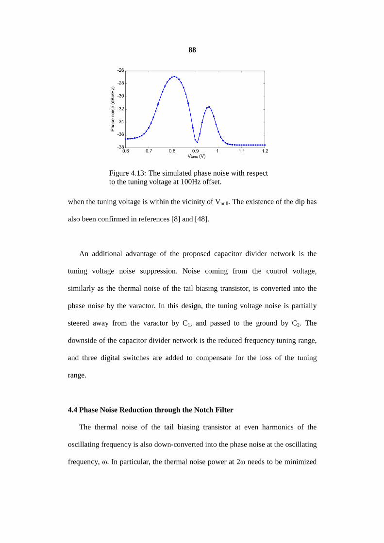
88
when the tuning voltage is within the vicinity of Vnull. The existence of the dip has
also been confirmed in references [8] and [48].
An additional advantage of the proposed capacitor divider network is the
tuning voltage noise suppression. Noise coming from the control voltage,
similarly as the thermal noise of the tail biasing transistor, is converted into the
phase noise by the varactor. In this design, the tuning voltage noise is partially
steered away from the varactor by C1, and passed to the ground by C2. The
downside of the capacitor divider network is the reduced frequency tuning range,
and three digital switches are added to compensate for the loss of the tuning
range.
4.4 Phase Noise Reduction through the Notch Filter
The thermal noise of the tail biasing transistor at even harmonics of the
oscillating frequency is also down-converted into the phase noise at the oscillating
frequency, ω. In particular, the thermal noise power at 2ω needs to be minimized
Figure 4.13: The simulated phase noise with respect to the tuning voltage at 100Hz offset.

89
since the conversion gain is higher at 2ω compared to other even harmonics [45].
A filtering technique is proposed in Reference [17] to reduce the thermal noise
power at 2ω from entering the resonator, where the inductor and the capacitor
together form high impedance at 2ω such that the thermal noise of the tail
transistor within the vicinity of 2ω is isolated from the resonator.
In this work, a 2nd order notch filter is implemented as shown in Figure 4.14.
The noise transfer function is given by,
( )( )
2
2
1.
1nf nfAM Out
AM In nf nf nf nf
s L CS
S s L C sR C
ωω
−
−
+=
+ + (4.46)
At both the low and high frequencies, the magnitude of the transfer function
evaluates to unity. At the resonant frequency, the magnitude is zero. When the
resonant frequency of the notch filter matches 2ω, the thermal noise power of the
tail transistor within the vicinity of 2ω is greatly attenuated.
With the notch filter, the inductor is no longer directly connected between the
tail transistor and the resonator, where the inductor is replaced with Rnf. As a
Figure 4.14: The proposed 2nd order notch filter in this work.

90
result, the thermal noise associated with the series resistance of the inductor
which can enter the resonator is replaced with the thermal noise associated with
Rnf. While the ease of reducing the series resistance of the inductor is limited by
the required inductance to form the high impedance at 2ω, there is much more
freedom in adjusting Rnf, where Rnf affects only the bandwidth of the notch filter.
Therefore, Rnf can be adjusted to a much smaller value which enlarges the
bandwidth of the notch filter. The upper limit on the expanding of the bandwidth
is that the lower cut-off frequency of the notch filter cannot approach the vicinity
of ω such that the signal power shall not be affected.
The series resistance of the inductor in the notch filter is connected in series
with Cnf and Lnf. At both the low and high frequencies, Cnf and Lnf behave as open
circuit, respectively. When the thermal noise is modeled as a current source, it is
connected to an open circuit at the low and high frequencies which prevents
continuous current flow. At 2ω, the combined impedance of Cnf and Lnf is zero,
which provides a short circuit to the power supply for the noise current.
Figure 4.15: The simulated VCO phase noise spectrums.

91
Therefore, the power spectral density of the inductor series resistance is reduced
in general.
The simulated phase noise with SpectreRF in TSMC0.18 µm technology is
shown in Figure 4.15. It is evident that the phase noise at lower frequency offset
has been improved by 15dB, and 5dB at higher frequency offset.
4.5 Experimental Measurement Results
Two VCOs are fabricated using TSMC 0.18µm technology, which provides 6
metal layers. The die photo is shown in Figure 4.16, and the die area is
2.2×1.8mm2. Both VCOs are implemented with the top-biased complementary
structure as shown in Figure 4.1(b). VCO1 consists of both the capacitor divider
network and the 2nd order notch filter while VCO2 is implemented with only the
capacitor divider network. The component parameters of the two VCOs are
summarized in Table 4.1.
Table 4.1: Circuit design parameters
Values Values Rnf 10Ω W1/L1 800µm/1µm Cnf 1.75pF W2-3/L2-3 240µm/0.18µm C1-2 5pF W4-5/L4-5 120µm/0.18µm C3 15pF W6-7/L6-7 800µm/3µm C4 2.5pF W8/L8 50µm/0.18µm R1 500Ω
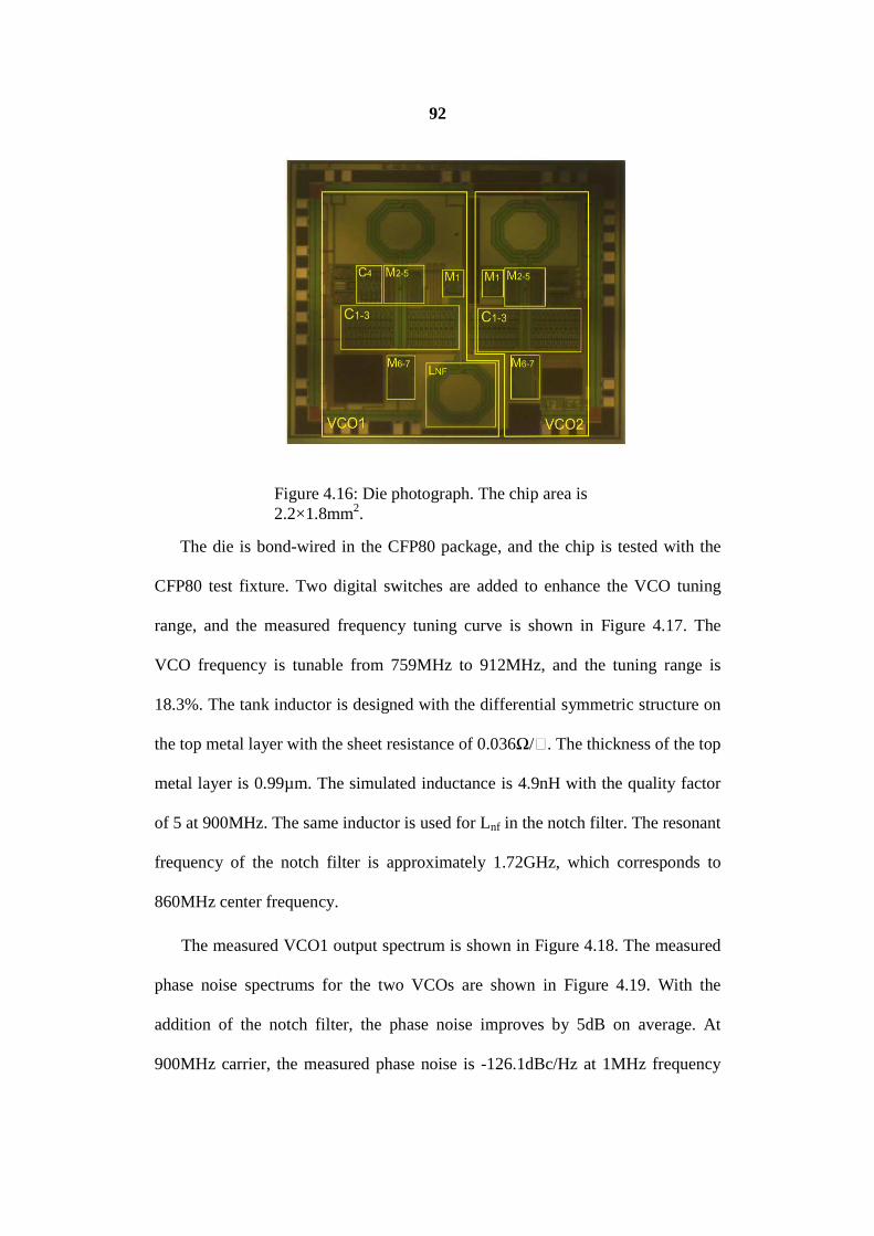
92
The die is bond-wired in the CFP80 package, and the chip is tested with the
CFP80 test fixture. Two digital switches are added to enhance the VCO tuning
range, and the measured frequency tuning curve is shown in Figure 4.17. The
VCO frequency is tunable from 759MHz to 912MHz, and the tuning range is
18.3%. The tank inductor is designed with the differential symmetric structure on
the top metal layer with the sheet resistance of 0.036Ω/. The thickness of the top
metal layer is 0.99µm. The simulated inductance is 4.9nH with the quality factor
of 5 at 900MHz. The same inductor is used for Lnf in the notch filter. The resonant
frequency of the notch filter is approximately 1.72GHz, which corresponds to
860MHz center frequency.
The measured VCO1 output spectrum is shown in Figure 4.18. The measured
phase noise spectrums for the two VCOs are shown in Figure 4.19. With the
addition of the notch filter, the phase noise improves by 5dB on average. At
900MHz carrier, the measured phase noise is -126.1dBc/Hz at 1MHz frequency
Figure 4.16: Die photograph. The chip area is 2.2×1.8mm2.
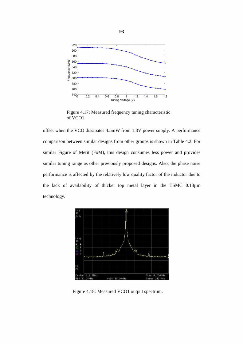
93
offset when the VCO dissipates 4.5mW from 1.8V power supply. A performance
comparison between similar designs from other groups is shown in Table 4.2. For
similar Figure of Merit (FoM), this design consumes less power and provides
similar tuning range as other previously proposed designs. Also, the phase noise
performance is affected by the relatively low quality factor of the inductor due to
the lack of availability of thicker top metal layer in the TSMC 0.18µm
technology.
Figure 4.17: Measured frequency tuning characteristic of VCO1.
Figure 4.18: Measured VCO1 output spectrum.

94
4.6 Conclusions
A low power LC-VCO design is proposed, designed, and fabricated in TSMC
0.18 µm technology. The design reduces the up-conversion effect of the flicker
noise due to the tail biasing transistor through a new capacitor divider varactor
configuration. A notch filter is added between the biasing transistor and the LC-
tank where the resonant frequency of the notch filter equals to twice the VCO
oscillating frequency. As a result, the thermal noise power at twice the oscillation
frequency is greatly reduced. A time-weighted approach is used to model the
effective capacitance experienced by the oscillating signal over the oscillation
period. Closed-form expressions of the effective capacitance are proposed, and
the calculated oscillation frequency based on the modeled effective capacitance is
in good agreement with the simulation results. Also, based on the modeled
effective capacitance, it is mathematically verified that the flicker noise due to the
tail biasing transistor is suppressed. The proposed design consumes less power
compared to other designs with similar FoM.
Figure 4.19: Measured phase noise of the two VCOs at 900MHz.

95

96
CHAPTER 5: GENERAL-PURPOPSE HIGH-SPEED
INTEGRATED LOCK-IN AMPLIFIER WITH 30Db
DYNAMIC RESERVE AT 20MHz
This Chapter describes the design and implementation of a general-purpose
high-speed integrated LIA. Instrumentation LIAs such as the SR830 LIA in [59]
are widely used for signal detection in many general laboratory settings, where
the signal frequency is less than 100kHz. The advantages of the instrumentation
LIAs include setup convenience, large input and output signal dynamic range,
large frequency range and huge dynamic reserve. The drawbacks include high
equipment cost and huge power consumptions, where system integration with
other devices is greatly limited. On-chip integrated LIAs have also been designed
such as in [60][61] for a few targeted applications, where the silicon area and
power consumption of the LIA chip are suitable for integration purpose.
LIAs designed for high-speed applications where the signal frequency is in
the MHz range are much less common. Instrumentation LIAs offered by Stanford
Research Systems Inc. [62] and Zurich Instruments Inc. [63] offer excellent
performance at the expense of large size and huge power consumption. To the
best knowledge, they are the only commercial available high-speed LIAs. To date,
on-chip integrated high-speed LIAs are not reported in literature. In this project, a
general-purpose high speed integrated LIA is reported where the frequency
operating range is between 15 and 20MHz. The proposed design does not require

97
any off-chip components and achieves 30dB dynamic reserve with power
consumption of 37mW.
Low-speed LIAs typically use the phase-sensitive detection (PSD) technique
to extract the amplitude and the phase of the input signal as illustrated in Figure
5.1. The input signal is usually the sum of the signal to be detected and the noise
with the spectrum spanning over a frequency range. After pre-amplification and
filtering, the input signal is applied to two mixers. The reference signal with the
same frequency as the input signal is also applied to the mixers. The reference
signal is phase-shifted by 90° before it is applied to the second mixer. The
corresponding signal spectrum is shown in Figure 5.2. The input signal with
frequency ω is embedded within noise with bandwidth BN. The reference signal is
usually generated by an on-chip oscillator, and the signal spectrum consists of
tones at ±ω, ±3ω, and so forth. The convolution of the two signals leads to the
tones at DC, ±2ω, ±4ω, and so forth. The tone at DC carries the information of the
input magnitude and phase, and is the signal of interest. A low-pass filter
following the mixer removes the undesired harmonics and the noise. The nth
Figure 5.1: The PSD technique used in low-speed LIA design.

98
harmonic of the reference signal folds the high-frequency noise down to the
baseband when 2nω<BN. Also, undesired tones at small frequency offset with
respect to the input signal are usually hard to filter out. Therefore, low-pass filter
with narrow bandwidth and faster roll-off is highly desired. For a first-order low-
pass filter with cut-off frequency f3dB, the SNR improvement due to PSD is given
by,
3
2.N
After BeforedB
BSNR SNR
fπ= (5.1)
BN is a modest approximation of the noise bandwidth as the total noise power is
increased due to noise folding. While low pass filter with narrow bandwidth
offers greater SNR improvement, the implementation usually requires extra large
passive components, which is disadvantageous for on-chip integration.
PLL technique has been widely used in the communication receivers to
recover signals embedded within noise. A PLL with small bandwidth averages the
phase error between the input signal and the oscillator signal, where the input
Figure 5.2: Signal spectrum of the time multiplication before and after the mixer.

99
random phase variation is greatly suppressed by the feedback loop. A PLL is a
well fit for on-chip integration, where highly integrated frequency synthesis and
data recovery circuits based on PLL are widely used in wireless and wire-line
applications. Also, PLL offers a huge frequency operating range from MHz to
GHz, and is well suited for high-speed applications. One disadvantage of the PLL
is that it can only keep track of the phase error of the input signal while the
random amplitude variation of the input signal is ignored. Therefore, PLL is only
used in the phase measurement of the proposed lock-in amplifier, while the
magnitude measurement is carried out with filters and time-average approach.
5.1 System Architecture
The architecture of the proposed lock-in amplifier is shown in Figure 5.3. The
input sinusoidal signal to be measured is denoted as
( )cos .SIG SIG SIGV A tω θ= + (5.2)
The design is able to measure the amplitude of VSIG with the Amplitude
Measurement circuitry, and the relative phase difference between VSIG and VREF
with the Phase Measurement circuitry. The measured amplitude and phase signals
are denoted as VMAG and VPH as shown in Figure 5.3. A band-limited white noise
VNOISE with the bandwidth BN is superimposed on top of the input signal through
an analog adder, where the signal-to-noise ratio is denoted as SNRin. A band-pass
filters with bandwidth fBPF follows the analog adder, and improves SNRin to,
2
,NAfter BPF in
BPF
BSNR SNR
fπ− = (5.3)

100
where, fBPF is much smaller than BN. The simulated waveforms of VSIG and VBPF
are shown in Figure 5.4. For an arbitrary cycle j, the amplitude and phase of VSIG
are denoted as ASIG,j and θSIG,j, where both ASIG,j and θSIG,j vary from cycle to
cycle due to VNOISE. A voltage amplifier increases the signal swing of VBPF to rail-
to-rail as shown in Figure 5.4. A duty cycle adjustment circuit changes the duty
cycle of VAMP from 50% to 25%. Since both VAMP and VCLK inherits the same
θSIG,j from VBPF, the falling edges of VCLK approximately sample the peak
amplitude of VBPF as shown in Figure 5.4. Multi-phase clock signals, Φ are
generated from VCLK, and control a switch-capacitor integrator. The integrator
calculates the average value (VMAG) of ASIG over N cycles, where,
,1
1.
N
MAG SIG jj
V AN =
= ∑ (5.4)
Figure 5.3: The system architecture of the proposed integrated lock-in amplifier.

101
VAMP is also used as the reference signal of a PLL with noise bandwidth BPLL.
The PLL attenuates the out-of band random phase variation of VAMP, and further
improves SNRAfter-BPF to,
.2
BPFAfter PLL After BPF
PLL
fSNR SNR
B
π− −= (5.5)
The phase difference between VPLL and VREF are compared by a phase detector.
The output of the phase detector controls a charge pump, which generates the ICP
signal where the time-averaged magnitude of ICP is proportional to the phase
difference between VPLL and VREF. ICP over N multiple periods are added and
averaged by a current integrator, and the output signal VPH is given by,
( ),1
,N
PHPH SIG j REF
j
KV
Nθ θ
=
= −∑ (5.6)
Figure 5.4: Simulated transient voltage waveforms for amplitude measurement. First: VSIG (red) and VBPF (black). Second: VAMP. Third: VCLK.

102
where, KPH depends on the gain of the current integrator and will be derived later
on. N for both the amplitude and phase measurements can be conveniently set by
the digital counters.
5.2 Component Descriptions of the Amplitude Measurement Circuitry
This section describes the circuit components of the amplitude measurement
section of the LIA in Figure 5.3. It takes VSN as the input, and generates a DC
signal VMAG, where the magnitude of VMAG is proportional to the amplitude of
VSIG.
5.2.1 Band-Pass Filter
The circuit schematic of the gm-C band-pass filter is shown in Figure 5.5 [64].
The center frequency and quality factor are given by,
2 3
1 2
,m mC
g g
C Cω = (5.7)
and
Figure 5.5: Schematic of the band-pass filter. Design parameters: C1=64pF, C2=4pF, gm1=gm2=gm3
=4gm4=1.59mA/V.

103
2 3 1
4 2
.m m
m
g g CQ
g C= (5.8)
The feedback loop formed by trans-conductors two and three will oscillate for
moderate gm values, and trans-conductor one is able to stabilize the output voltage
for large gm1 values at the cost of reduced filter quality factor. However, the
effectiveness of trans-conductor one degrades as gm1 decreases. Therefore, trans-
conductor four is added to make the filter quality factor independent of gm1. The
center frequency is tuned by changing the biasing current of trans-conductor
three, which effectively varies gm3. By setting gm2=4gm4 and C1=16C2, quality
factor over 20 is achieved while the frequency tuning range is from 14-22MHz.
5.2.2 Amplifier
The voltage amplifier following the band-pass filter increases the signal swing
to rail-to-rail. Since VCLK samples the peak value of VBPF, it is critical that the
amplifier bandwidth is high enough such that no phase shift exists between VBPF
and VAMP. As a result, amplifier with common source configuration is employed
due to its high bandwidth and large output dynamic range.
5.2.3 Duty-Cycle Adjustment and Clock Generation
The duty cycle of VCLK is adjusted from 50% to 25% through the circuitry
shown in Figure 5.6(a). An inverter-based voltage-controlled delay line (VCDL)
as shown in Figure 5.6(b) provides half of a signal period time delay. An AND
gate produces VCLK, which is phase aligned with VAMP.
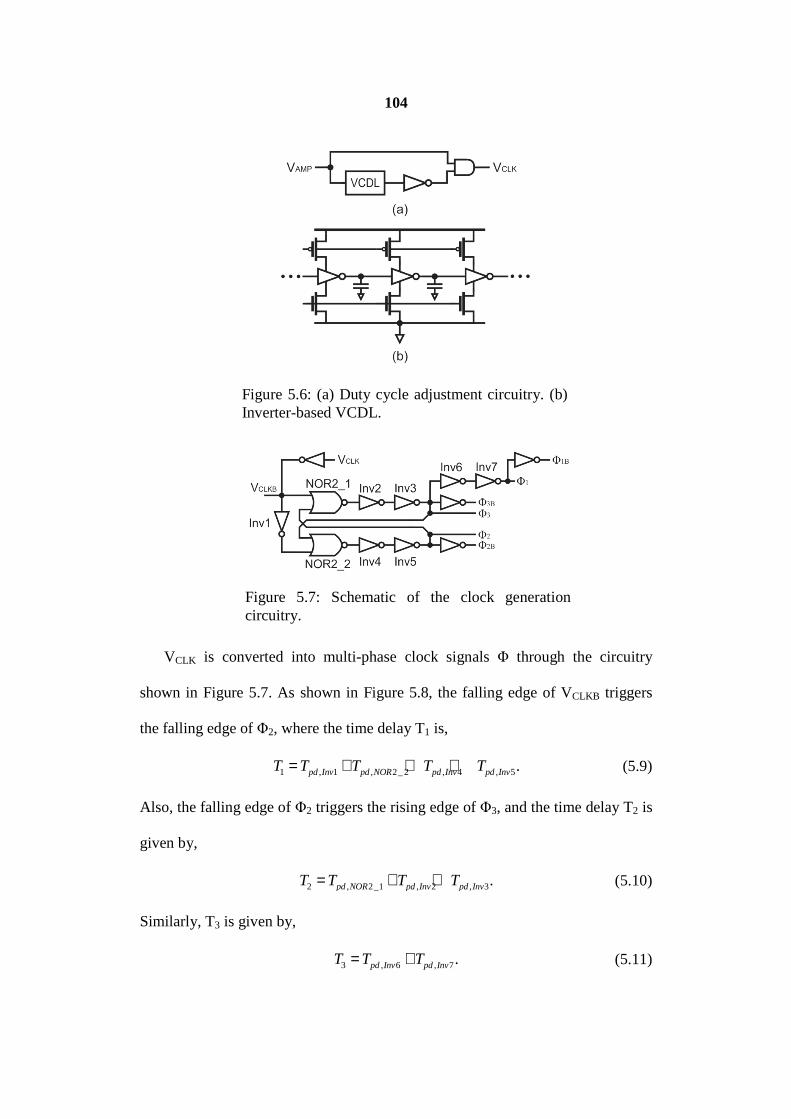
104
VCLK is converted into multi-phase clock signals Φ through the circuitry
shown in Figure 5.7. As shown in Figure 5.8, the falling edge of VCLKB triggers
the falling edge of Φ2, where the time delay T1 is,
1 , 1 , 2_ 2 , 4 , 5.pd Inv pd NOR pd Inv pd InvT T T T T= + + + (5.9)
Also, the falling edge of Φ2 triggers the rising edge of Φ3, and the time delay T2 is
given by,
2 , 2_1 , 2 , 3.pd NOR pd Inv pd InvT T T T= + + (5.10)
Similarly, T3 is given by,
3 , 6 , 7.pd Inv pd InvT T T= + (5.11)
Figure 5.6: (a) Duty cycle adjustment circuitry. (b) Inverter-based VCDL.
Figure 5.7: Schematic of the clock generation circuitry.
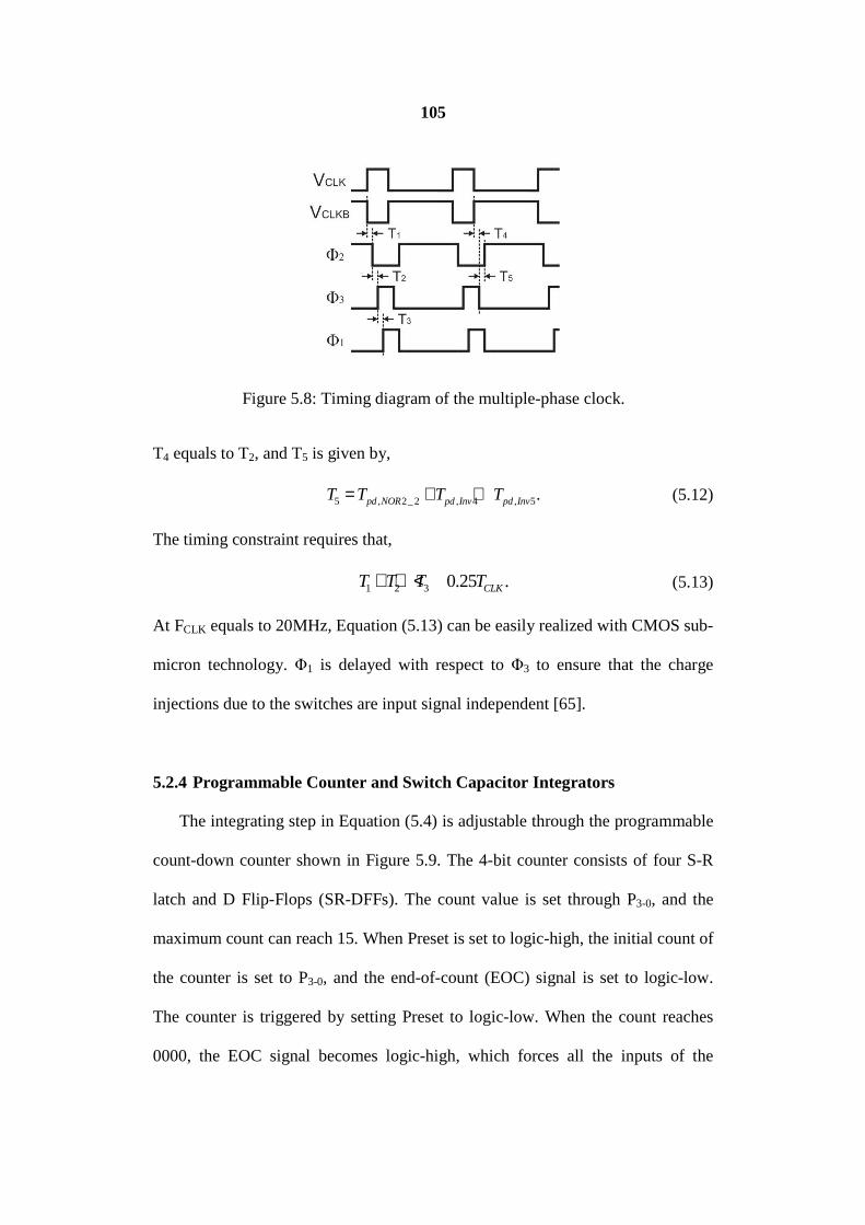
105
T4 equals to T2, and T5 is given by,
5 , 2_ 2 , 4 , 5.pd NOR pd Inv pd InvT T T T= + + (5.12)
The timing constraint requires that,
1 2 3 0.25 .CLKT T T T+ + < (5.13)
At FCLK equals to 20MHz, Equation (5.13) can be easily realized with CMOS sub-
micron technology. Φ1 is delayed with respect to Φ3 to ensure that the charge
injections due to the switches are input signal independent [65].
5.2.4 Programmable Counter and Switch Capacitor Integrators
The integrating step in Equation (5.4) is adjustable through the programmable
count-down counter shown in Figure 5.9. The 4-bit counter consists of four S-R
latch and D Flip-Flops (SR-DFFs). The count value is set through P3-0, and the
maximum count can reach 15. When Preset is set to logic-high, the initial count of
the counter is set to P3-0, and the end-of-count (EOC) signal is set to logic-low.
The counter is triggered by setting Preset to logic-low. When the count reaches
0000, the EOC signal becomes logic-high, which forces all the inputs of the
Figure 5.8: Timing diagram of the multiple-phase clock.

106
NOR-4 gate to logic-low. Therefore, EOC is kept logic-high thereafter until
Preset becomes logic-high again.
After the instance where VCLK causes the counter output to be 0000, the
propagation delay through DFF1, NOR4, and MUX1,2 cannot be longer than the
period of VCLK as
, 1 , 1 , 2 , 4 .pd DFF pd MUX pd MUX pd NOR CLKT T T T T+ + + < (5.14)
Since TCLK evaluates to 50ns, Equation (5.14) can be easily satisfied with CMOS
sub-micron technology.
The schematic of the switch-capacitor integrator is shown in Figure 5.10(a).
When the EOC signal is logic-low, the clock signal Φ1,2,3 control the switches of
the integrator. After EOC becomes logic-high, all the switches are turned off and
VMAG is held constant. A high-pass filter consisting of CHF and RHF is added to
ensure that only the AC magnitude of VBPF is integrated while the DC component
Figure 5.9: Schematic of the 4-bit programmable counter in the magnitude measurement circuitry.

107
is blocked. When Preset is set to logic-high, VMAG is forced to be VAGND. When
Preset becomes logic-low, VMAG becomes
1,
12
N
MAG AGND SIG jj
CV V A
C =
= + ∑ (5.15)
after N cycles.
During the integrating phase of the operation, approximately 7τOPA is required
for the OPAMP output to settle within 0.1% of the final value [66] where, τOPA is
the time constant of the OPAMP. Since the time duration allocated to the
integrating phase is 0.75TCLK, if the final value is required to settle within
0.4TCLK, τOPA should be less than 2.857ns. Since,
Figure 5.10: (a) Schematic of the switch-capacitor integrator. PMOS and NMOS switches: W/L=2µm/0.18µm. C1=C2=2pF. (b) Schematic of the integrator OPAMP. Component parameters: C1=1pF, W1,6=120µm, W2-
3=75µm, W4-5=12µm, W7=24µm, L1-7=0.18µm.

108
1
,OPAUGB
τβω
= (5.16)
where
2
1 2
,C
C Cβ =
+ (5.17)
and ωUGB is the unity-gain bandwidth of the OPAMP [66], ωUGB should be larger
than 111.4MHz when C1 equals to C2. This is achieved through the OPAMP
shown in Figure 5.10(b). ωUGB is designed to be 1.82GHz, more than a decade
above the required ωUGB.
5.3 Components Descriptions of the Phase Measurement Circuitry
This section describes the implementation of the phase measurement circuit of
the LIA as shown in Figure 5.3. VAMP is taken as the input of the PLL. The output
signal VPH is a DC voltage where the magnitude is proportional to the phase
difference between VSIG and VREF.
5.3.1 Phase-Locked Loop
The structure of the fractional-N phase-locked loop is shown in Figure 5.11.
The reference signal of the PLL is VAMP where the random phase variation of
VAMP due to VNOISE can be filtered out by the low-pass characteristic of the PLL.
The transfer function of the PLL is given by,
( )
( ) ,PD VCOPLL
REF PD VCO
K K F s
sN K K F s
θθ
=+
(5.18)

109
where, KPD, KVCO, F(s) and N represent the gain of the phase detector, the gain of
the VCO, the loop filter transfer function, and the feedback division value,
respectively. At low frequency offset, the random phase noise passes to the output
un-attenuated. As the frequency increases beyond the PLL loop bandwidth, the
PLL can no longer track the reference phase variation thus the phase noise is
effectively filtered at higher frequency offset.
5.3.1.1 The Phase Frequency Detector and Charge Pump
The schematic of the PFD and the charge pump are shown in Figure 5.12 and
Figure 5.13 respectively. The PFD is implemented based on CMOS logic, which
is fully functional for the intended input frequency range. A well-known issue
encountered with the PFD is the dead-zone problem, where the PFD and the
charge pump cannot supply sufficient output current to the loop filter when the
time difference between the reference signal and the feedback signal is smaller
than the switch delay of the charge pump [8]. The reduced gain of the PFD
directly leads to reduced loop bandwidth, which could make the PLL less stable.
Figure 5.11: Schematic of the fractional-N PLL.

110
A common approach to resolve this issue is to add extra time delay in the PFD
such that the propagation delay of the PFD is longer than the switch delay of the
charge pump. The apparent drawback of this approach is the addition of the extra
phase error.
Figure 5.12: Schematic of the phase-frequency detector.
Figure 5.13: Schematic of the differential charge pump.

111
The UP and DN signal of the PFD are converted into eight control signals for
the charge pump (identical circuitry for UP and DN signal) as shown in Figure
5.12(b) [67]. The control signals of the charge pump switches should not turn
both branches off at any time instance in order to avoid the glitch at the drains of
the biasing transistors. Therefore, the falling edge of VUND lags VUP, and the
rising edge of VUND leads VUP as shown in Figure 5.14. To achieve the require
timing waveforms, the threshold voltages of the inverters are adjusted as shown in
Figure 5.12(b), where Inverter-H has high switching threshold voltage by making
the aspect ratio of the PMOS transistor much larger than that of the NMOS
transistor, and vice versa. Also, cross-coupled inverters are used to ensure the
phase alignment between VUP and VUN. The switch sizes are made minimum to
reduce the charge injection effect. A voltage follower in Figure 5.13 is added to
limit the charge sharing effect [8].
5.3.1.2 The Loop Filter
Since the PLL can only filter phase variation at frequency offset above the
PLL loop bandwidth, lower PLL loop bandwidth is highly desired in the intended
Figure 5.14: Timing diagram of charge pump switch control.

112
LIA application. Large passive capacitor is usually required to achieve low PLL
bandwidth, and is not suitable for on-chip integration. The dual-path loop filter
proposed in [68] achieves the same loop bandwidth and dynamic but with much
smaller capacitance value as shown in Figure 5.15. The loop filter requires two
charge pumps with output currents ICP and BICP. The first path of the loop filter
consists of a current integrator, and the second path is a low-pass filter. The sum
of the two paths is passed to another low-pass filter to attenuate the reference
spur. The transfer function of the loop filter is given by,
( )( )4
11( ) ,
1 1Z
Z P
sF s
sC s s
ττ τ
+=+ +
(5.19)
where, τZ=BRPCZ, τP=RPCP and τ4=R4C4. Therefore, for the same zero location τZ,
the required capacitance CZ can be reduced by B times. The structure of the
amplifier in the integrator path is a differential pair. The analog adder proposed in
[69] is implemented in this design. The loop filter parameters are summarized in
Table 5.1.
Figure 5.15: Schematic of the dual-path loop filter.

113
Table 5.1: Summary of the loop filter parameters
Component Value
ICP 26µA B 10 CZ 163pF RP 7.8kΩ CP 68.4pF R4 3.9kΩ C4 137pF
From Equation (5.19), the zero frequency is 12kHz, and the frequency of the two
poles is 300kHz. The PLL loop bandwidth is given by
,2
CP VCO P P Z
Z
I K R C BCK
N Cπ+= (5.20)
which evaluates to 52.1kHz when KVCO equals to 78.4MHz/V. Therefore, KτZ and
KτP are approximately 4.3 and 0.174, respectively.
The PLL open-loop response is simulated as shown in Figure 5.16. At low
frequency, the magnitude response decreases at -40dB/dec. The zero at τZ
Figure 5.16: Simulated bode plot of the PLL open-loop response.

114
increases the slope to -20dB/dec, and the two poles at τP and τ4 decrease the slope
to -60dB/dec. At the crossover frequency, the phase margin is approximately 57°.
5.3.1.3 LC-VCO
For low power application, the top-biased complementary LC-VCO is
implemented in this design as shown in Figure 5.17 due to its better phase noise
performance. L1 is increased several times beyond the minimum length to reduce
the flicker noise power of the biasing transistor. W2-3/W4-5 is adjusted to ensure
the half-cycle symmetry of the oscillating signal for better phase noise
performance [70]. L2-5 is kept at the minimum length to reduce the impact of the
M2-5 oxide capacitance on the frequency tuning range. L6 is made large to extend
the frequency tuning range at the expense of the degraded phase noise.
Figure 5.17: Schematic of the top-biased complementary LC-VCO. Component parameters: W1=250µm, W2-
3=240µm, W4-5=120µm, W6-7=800µm, L1=1µm, L2-
5=0.18µm, L6-7=3µm, C1-2=5pF, C3=15pF.
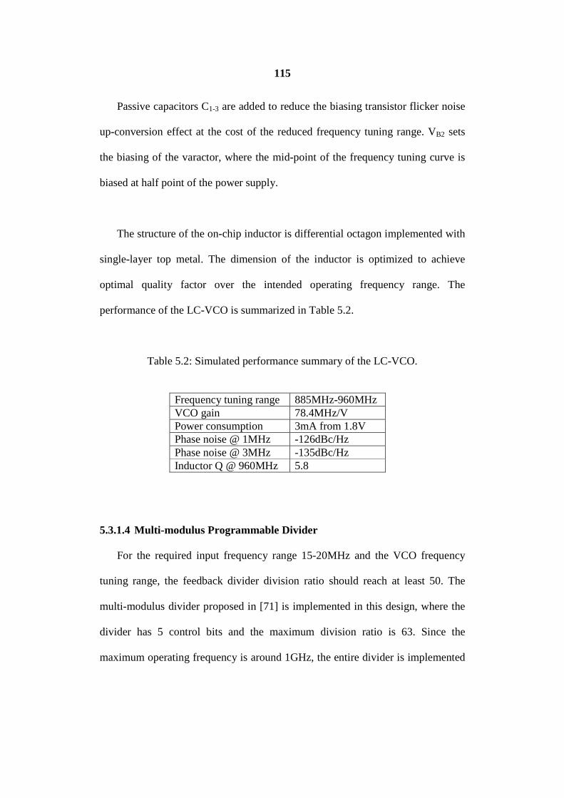
115
Passive capacitors C1-3 are added to reduce the biasing transistor flicker noise
up-conversion effect at the cost of the reduced frequency tuning range. VB2 sets
the biasing of the varactor, where the mid-point of the frequency tuning curve is
biased at half point of the power supply.
The structure of the on-chip inductor is differential octagon implemented with
single-layer top metal. The dimension of the inductor is optimized to achieve
optimal quality factor over the intended operating frequency range. The
performance of the LC-VCO is summarized in Table 5.2.
Table 5.2: Simulated performance summary of the LC-VCO.
Frequency tuning range 885MHz-960MHz VCO gain 78.4MHz/V Power consumption 3mA from 1.8V Phase noise @ 1MHz -126dBc/Hz Phase noise @ 3MHz -135dBc/Hz Inductor Q @ 960MHz 5.8
5.3.1.4 Multi-modulus Programmable Divider
For the required input frequency range 15-20MHz and the VCO frequency
tuning range, the feedback divider division ratio should reach at least 50. The
multi-modulus divider proposed in [71] is implemented in this design, where the
divider has 5 control bits and the maximum division ratio is 63. Since the
maximum operating frequency is around 1GHz, the entire divider is implemented

116
with CMOS logic for lower power consumption. The divider output is taken from
the same mod 2/3 block as the input signal for best phase noise performance.
5.3.1.5 ∆Σ Modulator
An all-digital 3rd-order 3-bit MASH ∆Σ modulator is designed as shown in
Figure 5.18. The three digital phase accumulators are implemented based on full
adders and DFFs. The transfer function is given by,
( )33 11 1 ,Y Xz q z− −= + − (5.21)
where, q1 is the quantization noise of the first accumulator. Since the MASH ∆Σ
modulator consists of three first order modulators, it is always stable while
providing higher order noise filtering.
The narrow PLL loop bandwidth leads to relatively slow settling time. To
improve the settling time, the VCO output frequency is held constant such that the
input frequency hopping is offset by the variation of the feedback fractional-
division ratio instead of the variation of the VCO frequency. For the 5MHz
Figure 5.18: Block diagram of the MASH ∆Σ modulator.

117
reference frequency range, 112 equal frequency increment ∆F is allocated such
that ∆F is approximately 45kHz. The frequency span of each increment ∆F is
( ), [20 , 20 1 ],SPAN mF F m F m= − ∆ ⋅ − ∆ ⋅ − (5.22)
where, m varies from 1 to 112. For the 3-bit MASH modulator, the resolution of
the fractional-division ratio is 1/8. Therefore, for each FSPAN,m, the corresponding
feedback division ratio is set to
45 ,8m
mD = + (5.23)
and the VCO output frequency is the product of FSPAN,m and Dm. The VCO
frequency with respect to the reference frequency plot is shown in Figure 5.19,
where the VCO frequency varies within ±15MHz over the targeted reference
frequency span. For any interested input frequency between 15-20MHz, the
corresponding Dm is applied to the coarse and fine control in Figure 5.11. The
VCO frequency is forced to be adjusted slightly to compensate for the limited
resolution of the MASH modulator, and the settling time of the PLL to lock to the
new reference frequency can be greatly improved.
Figure 5.19: VCO frequency variation with respect to the reference frequency due to variable feedback division ratio.
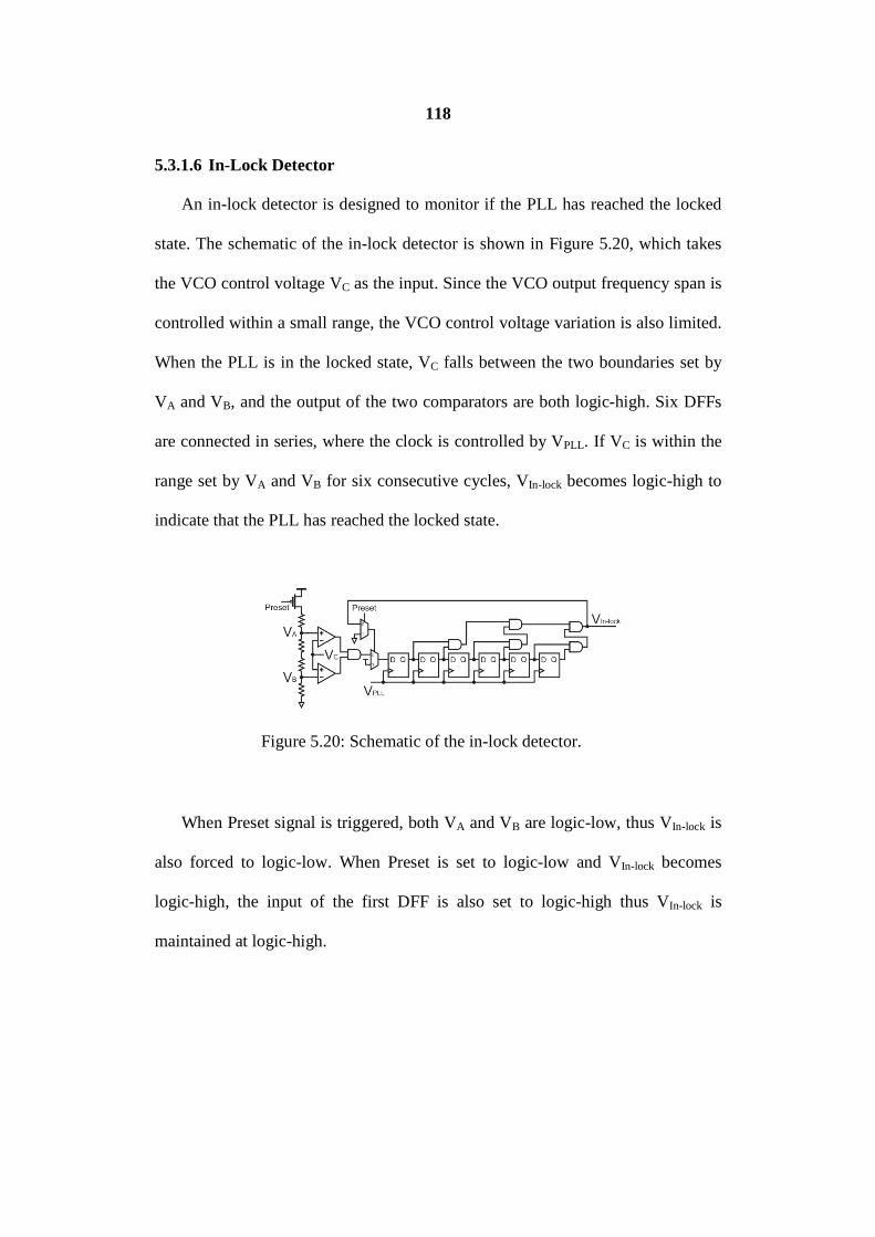
118
5.3.1.6 In-Lock Detector
An in-lock detector is designed to monitor if the PLL has reached the locked
state. The schematic of the in-lock detector is shown in Figure 5.20, which takes
the VCO control voltage VC as the input. Since the VCO output frequency span is
controlled within a small range, the VCO control voltage variation is also limited.
When the PLL is in the locked state, VC falls between the two boundaries set by
VA and VB, and the output of the two comparators are both logic-high. Six DFFs
are connected in series, where the clock is controlled by VPLL. If VC is within the
range set by VA and VB for six consecutive cycles, VIn-lock becomes logic-high to
indicate that the PLL has reached the locked state.
When Preset signal is triggered, both VA and VB are logic-low, thus VIn-lock is
also forced to logic-low. When Preset is set to logic-low and VIn-lock becomes
logic-high, the input of the first DFF is also set to logic-high thus VIn-lock is
maintained at logic-high.
Figure 5.20: Schematic of the in-lock detector.

119
5.3.2 Programmable Counter
The schematic of the 4-bit programmable counter is shown in Figure 5.21.
When VIn-lock is at logic-low, the initial conditions of the SR-DFFs are set to P3-0.
Therefore, EOC signal is set to logic-low. When VIn-lock is at logic-high and the
counter has reached the 0000 state, EOC becomes logic-high to maintain EOC at
logic-high. As a result, VPLLX and VREFX are set to logic-low to disable the down-
stream phase detector and charge pump.
5.3.3 Current Integrator
The phase difference between VPLL and VREF are measured by the phase
detector and the charge pump. The charge pump current ICP charges the current
integrator in Figure 5.22 for N period set by P3-0 of the programmable counter.
The final voltage VPH after N cycles is given by Equation (5.6), where,
.2
CPPH
REF
IK
f Cπ= (5.24)
Figure 5.21: Schematic of the 4-bit programmable counter in the phase measurement circuitry.

120
The same phase detector and charge pump in Figure 5.12 and Figure 5.13 are used
in the phase measurement circuitry.
5.4 Measurement Results
The designed high-speed integrated LIA is fabricated in TSMC 0.18µm
technology. The die micrograph is shown in Figure 5.23, where the chip area is
5mm2. The die is bond-wired in the CFP80 package provided by Canada
Microelectronics Corporation, and the chip is tested with the CFP80 testing
fixture. The reference signal and the LC-VCO output are bond-wired externally to
test the performance of the PLL. When the reference of the PLL is driven by a
high-purity external signal, the measured VCO phase noise is shown in Figure
5.24. The measured phase noise at 1MHz and 3MHz frequency offset are -
125dBc/Hz and -131dBc/Hz at 890MHz output frequency, respectively. The PLL
loop bandwidth is less than 100kHz, and the in-band phase noise is under -
80dBc/Hz.
Figure 5.22: Schematic of the current integrator.

121
Both VSIG and VNOISE in Figure 5.3 are supplied with external power supply.
At -30dB SNR and 20MHz input frequency, the measured transient response of
VMAG is shown in Figure 5.25. During the preset phase, Preset signal is set to
logic-high and VMAG is forced to be VAGND as described in Figure 5.10. During
the integration phase, Preset signal is set to logic-low, and the programmable
counter is enabled. Maximum 15 integrating steps increase VMAG to the DC
Figure 5.23: Die micrograph of the fabricated high-speed LIA in TSMC 0.18µm technology.
Figure 5.24: Measured phase noise of the LC-VCO at 890MHz output frequency.

122
voltage proportional to the amplitude of VSIG. During the EOC phase, the
switches of the switch-capacitor integrator are turned off, and VMAG is held
constant. The variation of VMAG with respect to the amplitude of VSIG is shown in
Figure 5.26. Approximately 300mV variation of VMAG corresponds to 600mV
variation of VSIG amplitude, which translates to 0.5V/V sensitivity.
Figure 5.25: Measured transient waveforms at the output of the magnitude measurement circuitry. Top: 100mV input signal amplitude. Bottom: 700mV input signal amplitude. Yellow: VMAG. Blue: Preset signal.

123
Also, the measured transient response of VPH at 20MHz input frequency is
shown in Figure 5.27. The measured VPH with respect to the phase difference
between VSIG and VREF is shown in Figure 5.28, where VPH varies approximately
182mV for 60 degrees of phase difference. The sensitivity of the phase
measurement circuitry is 3mV/degree at -30dB SNR.
The performance of the high-speed LIA is compared with the existing designs
(including integrated low-speed LIAs and commercial large-sized high-speed
LIAs) in Table 5.3. Compared to the low-speed integrated LIAs from
[21][22][72], the proposed LIA provides a decent output dynamic range while
consuming relatively equivalent amount of power. The commercial large-sized
high-speed instrumentation LIA in [62] well exceeds the dynamic reserve and
output dynamic range performance compared to the proposed design. On the other
hand, the proposed design offers an on-chip integrated approach to realize the
magnitude and phase detection capability at much lower power consumption.
Figure 5.26: Measured DC output voltage with respect to the input signal amplitude.
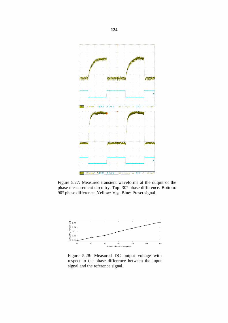
124
Figure 5.27: Measured transient waveforms at the output of the phase measurement circuitry. Top: 30° phase difference. Bottom: 90° phase difference. Yellow: VPH. Blue: Preset signal.
Figure 5.28: Measured DC output voltage with respect to the phase difference between the input signal and the reference signal.

125
Table 5.3: Performance comparison with existing designs.
5.5 Conclusion
In this design, a general-purpose high-speed integrated LIA is designed. The
designed LIA consists of the magnitude and phase measurement circuitry
components to extract the input signal magnitude and phase where the SNR can
be as worse as -30dB. The magnitude measurement circuitry relies on the band-
pass filter and a current integrator to generate the VMAG signal where VMAG is
directly proportional to the input signal amplitude. The phase measurement
circuitry uses a low-bandwidth PLL and current integrator to generate the VPH
where VPH is directly proportional to the phase difference between the input signal
and the reference signal. The designed LIA is fully integrated and requires no off-
chip components. It consumes 37mW of power while providing reasonable output
dynamic range, and magnitude and phase measurement sensitivity.
Frequency Technology Dynamic reserve
Power consumption
Output Range
[21] 20kHz CMOS 0.7µm
- 25mW 0.3V-0.55V
[22] 30kHz CMOS 0.35µm
40dB 110mW -0.2V-0.4V
[72] 1kHz CMOS 0.18µm
- 2mW 1.04V-1.18V
[62] 25kHz-200MHz
- 80dB 70W 100nV-1V
This Work
15-20MHz CMOS 0.18µm
30dB 37mW 0.54V-0.85V

126
CHAPTER 6: FUTURE WORK
The low-speed LIA for fluorescence signal detection proposed in Chapter 2
targets on signal magnitude extraction of the input optical signal. Phase extraction
between the input signal and the reference signal is also desired, where phase
sensitive detection technique can be applied.
The proposed time-average approach to model the LC-VCO oscillating
frequency characteristic in Chapter 4 has assumed that the oscillating signal is a
perfect sine wave, where only the fundamental tone exists. In reality, even-order
harmonics of the oscillating signal also exist due to the variable capacitance of the
varactor. To improve the accuracy of the proposed model, the impact of the even-
order harmonics on the oscillating frequency also needs to be modeled and
analyzed. The significance of improving the oscillating frequency model is to gain
more practical insight on VCO phase noise improvement. The harmonics induced
from different noise sources contribute to the VCO phase noise, and no closed-
form expressions of the harmonics as functions of VCO design parameters exist in
the literature yet. Therefore, the designers mainly rely on experience and general
rule of thumbs to obtain desired VCO phase noise performance. If precise
mathematical expressions of output signal harmonics are developed, noise sources
and their respective contributions are transparent, and phase noise optimization
can be carried out with much less effort and great precision.
127
The high-speed integrated LIA proposed in chapter 5 has been designed and
tested for electrical signals, where the input signals are generated from
instrumentation power supply. To apply the designed LIA in more application-
specific fields, the interface between the LIA chip and the detecting sensor is
required. Since the minimum detectable voltage of the LIA chip is in the mV
range, pre-filtering and amplification of the sensor signal are mandatory. Also, the
input detectable range is from 100mV to 700mV. This can be greatly improved
compared to the input detectable range of the commercial instrumentation LIA,
which falls within the microvolt range. To accommodate such small input voltage,
ultra low-noise and high gain amplifiers are required to improve the signal power.
Also, the LIA dynamic reserve has large room for improvement, where better
performance of electronic components are required. In particular, filters with
much higher quality factors are mandatory.

128
REFERENCES
[1] C. Lo and H. Luong, "A 1.5-V 900-MHz monolithic CMOS fast-switching frequency synthesizer for wireless applications," Symposium on VLSI Circuits, pp. 238-241, 2000.
[2] H. Rategh, H. Samavati, and T. Lee, "A CMOS frequency synthesizer with an injection-locked frequency divider for a 5-GHz wireless LAN receiver," IEEE Journal of Solid-State Circuits, vol. 35, no. 5, pp. 780-787, May 1993.
[3] H W. Yan and H. Luong, "A 2-V 900-MHz monolithic CMOS dual-loop frequency synthesizer for GSM receivers," IEEE Journal of Solid-State Circuits, vol. 36, no. 2, pp. 204-216, Feb. 2001.
[4] L. Chih-Fan and L. Shen-Iuan, "40 Gb/s transimpedance-AGC amplifier and CDR circuit for broadband data receivers in 90 nm CMOS," IEEE Journal of Solid-State Circuits, vol. 43, no. 3, pp. 642-655, Feb. 2008.
[5] L. Rodoni, G. von Buren, A. Huber, M. Schmatz, and H. Jackel, "40 Gb/s transimpedance-AGC amplifier and CDR circuit for broadband data receivers in 90 nm CMOS," IEEE Journal of Solid-State Circuits, vol. 44, no. 7, pp. 1927-1941, July 2009.
[6] S. Kim, K. Lee, Y. Moon, D. Jeong, Y. Choi, and H. Lim, "A 960 Mbps/pin interface for skew-tolerant bus using low jitter PLL," IEEE Journal of Solid-State Circuits, vol. 32, no. 5, pp. 691-700, May 1997.
[7] Y. Kim, S. Lee, S. Bae, Y. Sohn, J, Lee, J. Choi, H. Park, and J. Sim, "An 8GB/s quad-skew-cancelling parallel transceiver in 90nm CMOS for high-speed DRAM interface," IEEE International Solid-State Circuits Conference, vol. 32, no. 5, pp. 136-138, Feb. 2012.
[8] A. Lacaita, S. Levantino, and C. Samori, Integrated Frequency Synthesizers for Wireless Systems. New York, NY: Cambridge University Press, 2007.
[9] F. Gardner, Phaselock Techniques, Phaselock Techniques. New York, NY: J. Wiley & Sons, Inc., 1977, 3rd edition, 2005.
[10] F. Gardner, "Charge-pump phase-lock loops," IEEE Transactions on Communications, vol. 28, no. 11, pp. 1849-1858, Nov. 1980.
[11] T. Riley, M. Copeland, and T. Kwasniewski, "Delta-sigma modulation in fractional-N frequency synthesis ," IEEE Journal of Solid-State Circuits, vol. 28, no. 5, pp. 553-559, May 1993.
[12] C. Yue and S. Wong, "On-chip spiral inductors with patterned ground shields for Si-based RF ICs," IEEE Journal of Solid-State Circuits, vol. 33, no. 5, pp. 743-752, May 1998.
[13] A. Niknejad and R. Meyer, “Analysis and optimization of monolithic inductors and transformers for RF ICs,” IEEE Custom Integrated Circuits Conference, pp. 375-378, May 1997.
[14] S. Yim, T. Chen, and K. Kenneth, "The effects of a ground shield on the characteristics and performance of spiral inductors," IEEE Journal of Solid-State Circuits, vol. 37, no. 2, pp. 237-244, Feb. 2002.

129
[15] J. Long and M. Copeland, "The modeling, characterization, and design of monolithic inductors for silicon RF IC's," IEEE Journal of Solid-State Circuits, vol. 32, no. 3, pp. 357-369, Mar 1997.
[16] D. Leeson, “A simple model of feedback oscillator noise spectrum,” Proceedings of the IEEE, vol. 54, no. 2, pp. 329–330, 1966.
[17] E. Hegazi, H. Sjöland, and A. Abidi, “A filtering technique to lower LC oscillator phase noise,” IEEE J. Solid-State Circuits, vol. 36, no. 12, pp. 1921-1930, Dec. 2001.
[18] S. Johnson, M. Thomas, and C. Kros, “Membrane capacitance measurement using patch clamp with integrated self-balancing lock-in amplifier,” Pflugers Arch - European Journal of Physiology, Vol. 443, No. 4, pp. 653-663, Feb. 2004
[19] M. Sonnaillon, R. Urteaga, F. Bonetto, and M. Ordonez, “Implementation of a high-frequency digital lock-in amplifier,” Canadian Conference on Electrical and Computer Engineering, pp. 1229-1232, May 2005.
[20] A. De Marcellis, G. Ferri, M. Patrizi, V. Stornelli, A. D'Amico, C. Di Natale, E. Martinelli, A. Alimelli, and R. Paolesse, “An integrated analog lock-in amplifier for low-voltage low-frequency sensor interface,” 2nd International Workshop on Advances in Sensors and Interface, pp. 1-5, June. 2007.
[21] A. Gnudi, L. Colalongo, and G. Baccarani, “Integrated lock-in amplifier for sensor applications,” Proc. Euro. Solid-State Circuits Conf., pp. 58-61, Sept. 1999.
[22] C. Azzolini, A. Magnanini, M. Tonelli, G. Chiorboli, and C. Morandi, “Integrated lock-in amplifier for contactless interface to magnetically stimulated mechanical resonators,” 3rd International Design and Technology of Integrated Systems in Nanoscale Era, pp. 1-6, Mar. 2008.
[23] G. Ferri, P. De. Laurentiis, A. D'Amico, and C. Di. Natale, “A low-voltage integrated CMOS analog lock-in amplifier prototype for LAPS applications,” Sensors Actuators A: Phys., Vol. 92, No. 1, pp. 263-272, August 2001.
[24] MODEL SR830 DSP lock-in Amplifier, Stanford Research Systems, 2006. [25] H. Goovaerts, J. Faes, E. Raaijmakers, and R. Heethaar, “A wideband high
common-mode rejection ratio amplifier and phase-locked loop demodulator for multi-frequency impedance measurement,” Medical and Biological Engineering Computing, Vol. 36. No. 6, pp. 761-767, Nov. 1998.
[26] M. Davenport, A. Titus, E. Tehan, T. Zunyu Tao, T. Ying Tang, R. Bukowski, and F. Bright, “Chemical sensing systems using xerogel-based sensor elements and CMOS photodetectors,” IEEE Sensors J., Vol. 4, No. 2, pp. 180-188, Apr. 2006.
[27] V. Chodavarapu, D. Shubin, R. Bukowski, A. Titus, A. Cartwright, and F. Bright, “CMOS-based phase fluorometric oxygen sensor system,” IEEE Trans. Circuits and Syst. I - Regular Papers, Vol. 54, No. 1, pp. 111-118, Jan. 2007.

130
[28] L. Yao, R. Khan, V. Chodavarapu, V. Tripathi, and F. Bright, “Sensitivity-enhanced CMOS phase luminometry system using xerogel-based sensors,” IEEE Trans. on Biomedical Circuits and Syst., Vol. 3, pp. 304-311, 2009.
[29] K. Su, Analog filters, Kluwer Academic Publishers, New York, 2nd edition, 2002.
[30] J. Zhang, K. Li, R. Wang, “A low voltage high frequency programmable Gm-C bandpass filter,” IEEE International Workshop on Anti-counterfeiting, Security, Identification, pp. 70-74, Apr. 2007.
[31] R. Best, Phase-locked loops: design, simulation, and applications, sixth edition, McGraw-Hill 2007.
[32] J. Maget, M. Tiebout, and R. Kraus, “MOS varactors with n- and p-type gates and their influence on an LC-VCO in digital CMOS,” IEEE J. Solid-State Circuits, vol. 38, no. 7, pp. 1139-1147, July 2003.
[33] B. Jung and R. Harjani, “High-frequency LC VCO design using capacitive degeneration,” IEEE J. Solid-State Circuits, vol. 39, no. 12, pp. 2359-2369, Dec. 2004.
[34] J. Kim, J. Shin, S. Kim, and H. Shin, “A wide-band CMOS LC VCO with linearized coarse tuning characteristics,” IEEE Trans. Circuits Syst. II, vol. 55, no. 5, pp. 399-403, May 2008.
[35] P. Andreani and S. Mattisson, “On the use of MOS varactors in RF VCO’s,” IEEE J. Solid-State Circuits, vol. 35, no. 6, pp. 905-910, June. 2000.
[36] R. Bunch and S. Raman, “Large-signal analysis of MOS varactors in CMOS-Gm LC VCOs,” IEEE J. Solid-State Circuits, vol. 38, no. 8, pp. 1325-1332, Aug. 2003.
[37] R. Pierret, Semiconductor Device Fundamentals. Prentice Hall, 2nd edition, 1995.
[38] A. Porret, T. Melly, C. Enz, and E. Vittoz, “Design of high-Q varactors for low-power wireless applications using a standard CMOS process,” IEEE J. Solid-State Circuits, vol. 35, no. 3, pp. 337-345, Mar. 2003.
[39] R. Muller and T. Kamins, Device Electronics for Integrated Circuits. New York, NY: J. Wiley & Sons, Inc., 1977, 2nd edition, 1986.
[40] S. Kurachi, T. Yoshimasu, N. Itoh, and K. Yonemura, “5-GHz band highly linear VCO IC with a novel resonant circuit,” Silicon Monolithic Integrated Circuits in RF System, Long Beach, CA, USA, pp. 285-288, 2007.
[41] H. Zhang, G. Chen, and Ning Li, “A 2.4-GHz linear-tuning CMOS LC voltage-controlled oscillator,” Design Automation Conference, Proceedings of the ASP-DAC, Asia and South Pacific, Shanghai, China, pp. 799-802 Vol. 2. 2005.
[42] J. Mira, T. Divel, S. Ramet, J. Begueret, and Y. Deval,, “Distributed MOS varactor biasing for VCO gain equalization in 0.13µm CMOS technology,” Radio Frequency Integrated Circuits (RFIC) Symposium, Fort Worth, TX, USA, pp. 131-134, 2004.
[43] A. Dec, H. Akima, K. Suyama, “A 5GHz LC VCO with extended linear-range varactor in purely digital 0.15um CMOS process,” Radio Frequency Integrated Circuits (RFIC) Symposium, Boston, MA, USA, pp. 567-570, 2009.

131
[44] B. Liang, D. Chen, H. Guo, B. Wang, and T. Kwasniewski, “Analyze and design 10-GHz 0.8-VDD -117dBc/Hz quadrature LC-VCO in 120nm CMOS technology,” International Conference on Green Circuits and Systems, Shanghai, China, pp. 420-423, 2010.
[45] J. Rael and A. Abidi, “Physical processes of phase noise in differential LC oscillators," Proc. Custom Integrated Circuits Conf., pp. 569-572, May 2000.
[46] A. Bonfanti, S. Levantino, C. Samori, and A. Lacaita, “A varactor configuration minimizing the amplitude-to-phase noise conversion in VCOs," IEEE Trans. Circuits and Syst. I – Regular Papers, vol. 53, no. 3, pp. 481-488, Mar. 2006.
[47] Y. Chen, V. Neubauer, Y. Liu, U. Vollenbruch, C. Wicpalek, T. Mayer, B. Neurauter, L. Maurer, Z. Boos, “A 9 GHz dual-mode digitally controlled oscillator for GSM/UMTS transceivers in 65 nm CMOS,” IEEE Asian Solid-State Circuits Conf., Jeju, Korea, pp. 432-435, Dec. 2001.
[48] E. Hegazi and A. Abidi, “Varactor characteristics, oscillator tuning curves, and AM-FM conversion,” IEEE J. Solid-State Circuits, vol. 38, no. 6, pp. 1033-1039, Jun. 2003.
[49] S. Levantino, C. Samori, A. Zanchi, and A. Lacaita, “AM-to-PM conversion in varactor-tuned oscillators,” IEEE Trans. Circuits and Syst. II, vol. 49, no. 7, pp. 509-513, July 2002.
[50] P. Andreani and A. Fard, “More on the 1/f2 phase noise performance of CMOS differential-pair LC-tank oscillators,” IEEE J. Solid-State Circuits, vol. 41, no. 12, pp. 2703-2712, Dec. 2006.
[51] H. Darabi and A. Abidi, “Noise in RF-CMOS mixers: A simple physical model,” IEEE J. Solid-State Circuits, vol. 35, no. 1, pp. 15-25, Jan. 2000.
[52] A. Berny, A. Niknejad, and R. Meyer, “A 1.8-GHz LC VCO with 1.3-GHz tuning range and digital amplitude calibration,” IEEE J. Solid-State Circuits, vol. 40, no. 4, pp. 909-917, Apr. 2005.
[53] J. Craninckx and M. Steyaert, “Low-noise voltage-controlled oscillators using enhanced LC-tanks,” IEEE Trans. Circuits and Syst. II, vol. 42, no. 12, pp. 794-804, Dec. 1995.
[54] B. D. Muer, M. Borremans, M. Steyaert, and G. Puma, “A 2-GHz low-phase-noise integrated LC-VCO set with flicker-noise up-conversion minimization,” IEEE J. Solid-State Circuits, vol. 35, no. 7, pp. 1034-1038, July 2000.
[55] H. Kim, C. Cha, S. Oh, M. Yang, and S. Lee, “A very low-power quadrature VCO with back-gate coupling,” IEEE J. Solid-State Circuits, vol. 39, no. 6, pp. 952-955, June 2004.
[56] P. Andreani, “A low-phase-noise low-phase-error 1.8GHz quadrature CMOS VCO,” IEEE ISSCC Dig. Tech. Papers, San Francisco, CA, pp. 228-229, 2002.
[57] A. Ismail and A. Abidi, “CMOS differential LC oscillator with suppressed up-converted flicker noise,” IEEE ISSCC Dig. Tech. Papers, San Francisco, CA, pp. 98-99, 2003.

132
[58] J. Bhattacharjee, D. Mukherjee, E. Gebara, S. Nuttinck, and J. Laskar, “A 5.8 GHz fully integrated low power low phase noise CMOS LC VCO for WLAN applications,” Radio Frequency Integrated Circuits (RFIC) Symposium, Seattle, WA, pp. 475-478, 2002.
[59] MODEL SR830 DSP Lock-In Amplifier, Stanford Research Systems, 2011. [60] X. Jiawei, G Meynants, and P. Merken, “Low-power lock-in amplifier for
complex impedance measurement,” 3rd International Workshop on Advances in sensors and Interfaces, pp. 110-114, Trani, Italy June 2009.
[61] A. De Marcellis, G. Ferri, A. D'Amico, C. Di Natale, E. Martinelli, “A fully-analog lock-in amplifier with automatic phase alignment for accurate measurements of ppb gas concentrations,” IEEE Sensors Journal, vol. 12, no. 5, pp. 1377-1383, May 2012.
[62] MODEL SR844 200MHz dual-phase lock-in amplifier, Stanford Research Systems.
[63] HF2LI lock-in amplifier, Zurich Instruments. [64] P. Furth, “A continuous-time bandpass filter implemented in subthreshold
CMOS with large-signal stability,” MWSCAS, pp. 264-267, Sacramento, CA, July 1997.
[65] B. Razavi, Design of analog CMOS integrated circuits. New York, NY: McGraw-Hill, Inc., 1st edition, 2001.
[66] D. Johns and K. Martin, Analog integrated circuit design. New York, NY: J. Wiley & Sons, Inc., 1977, 1st edition, 1997.
[67] B. D. Muer and M. Steyaert, “A CMOS monolithic ∆Σ-Controlled fractional-N frequency synthesizer for DCS-1800,” IEEE J. Solid-State Circuits, vol. 37, no. 7, pp. 835-844, July 2002.
[68] J. Craninckx and M. Steyaert, “A fully integrated CMOS DCS-1800 frequency synthesizer,” IEEE J. Solid-State Circuits, vol. 33, no. 12, pp. 2054-2065, Dec. 1998.
[69] F. Nabki, K. Allidina, F. Ahmad, P. V. Cicek, and M. N. El-Gamal, “A highly integrated 1.8 GHz frequency synthesizer based on a MEMS resonator,” IEEE J. Solid-State Circuits, vol. 44, no. 8, pp. 2154-2168, Aug. 2009.
[70] A. Hajimiri and T. Lee, “A general theory of phase noise in electrical oscillators,” IEEE J. Solid-State Circuits, vol. 33, no. 2, pp. 179-194, Feb. 1998.
[71] C.S. Vaucher, I. Ferencic, M. Locher, S. Sedvallson, U. Voegeli, and Z. Wang, “A family of low-power truly modular programmable dividers in standard 0.35-µm CMOS technology,” IEEE J. Solid-State Circuits, vol. 35, no. 7, pp. 1039-1045, July 2000.
[72] J. Xu, G. Meynants, and P. Merken, “Low-power lock-in amplifier for complex impedance measurement,” 3rd International Workshop on Advances in Sensors and Interfaces, pp. 110-114, June 2009.
